

Page 1
4-11
MT8870D/MT8870D-1
Integrated DTMF Receiver
Features
• Complete DT MF R eceiv er
• Low power co nsu mptio n
• Internal gai n sett ing a mplif ier
• Adjustable guard time
• Central office qua lity
• Power-down m o de
• Inhibit m o de
• Backward compatible with
MT8870C/M T88 70C -1
Applications
• Receiver system for British Telecom (BT) or
CEPT Spec (MT8870 D-1)
• Paging systems
• Repeater systems/mobile radio
• Credit card systems
• Remote con trol
• Personal com put ers
• Telephone answ erin g mach in e
Descript io n
The MT8870D/MT8870D-1 is a complete DTMF
receiver integrating both the bandsplit filter and
digital decoder functions. The filter section uses
switched capacitor techniques for high and low
group filters; the decoder uses digital counting
techniques to detect and decode all 16 DTMF tonepairs into a 4-bit code. External component count is
minimized by on chip provision of a differential input
amplifier, clock oscillator and latched three-state bus
interface.
Ordering Information
MT8870DE/DE-1 18 Pin Plastic DIP
MT8870DC/DC-1 18 Pin Ceramic DIP
MT8870DS/DS-1 18 Pin SOIC
MT8870DN/D N-1 20 Pin SSOP
MT8870DT /DT-1 20 Pin TSS OP
-40 °C to +85 °C
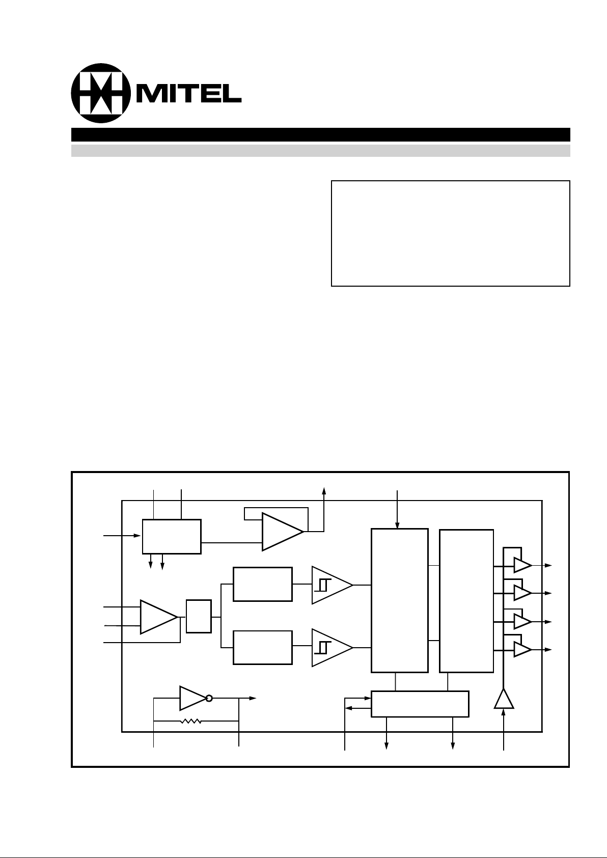
Figure 1 - Functional Block Diagram
PWDN
IN +
IN -
GS
OSC1 OSC2 St/GT ESt STD TOE
Q1
Q2
Q3
Q4
VDD VSS VRef INH
Bias
Circuit
Dial
Tone
Filter
High Group
Filter
Low Group
Filter
Digital
Detection
Algorithm
Code
Converter
and Latch
St
GT
Steering
Logic
Chip
Power
Chip
Bias
VRef
Buffer
Zero Crossing
Detectors
to all
Chip
Clocks
ISSUE 3 May1995
ISO2-CMOS
Page 2
MT8870D/MT8870D-1 ISO
2
-CMOS
4-12
Figure 2 - Pin Connections
Pin Description
Pin #
Name Description
18 20
11 IN+ Non-Inverting Op-Amp (Input).
2 2 IN- Inverting Op-Amp (Input).
33 GS Gain Select. Gives access to output of front end differential amplifier for connection of
feedback resistor.
44 V
Ref
Reference Voltage (Output). Nominall y VDD/2 is used to bias inputs at mid-rail (see Fig. 6
and Fig. 10).
55 INH Inhibit (Input). Logic high inhibi ts the det ecti on of tones represe nti ng characters A, B, C
and D. This pin input is internally pulled down.
66PWDNPower Down (Input). Active hig h. Powers down the device and inhi bits the oscillato r. This
pin input is internally pulled do wn.
78 OSC1Clock (Input).
89 OSC2Clock (Output). A 3.579545 MHz crystal connect ed between pins OS C1 and OSC2
completes the internal oscillator ci rcu it.
910 V
SS
Ground (Inpu t). 0V typical.
10 11 TOE Th ree S tate Output Ena bl e (Inp ut). Log ic high enables th e outpu ts Q1-Q4. This pin is
pulled up internally.
11-1412-15Q1-Q4 Three State Data (Outpu t). When enabled by TOE, provide the code corresponding to the
last valid tone-pair received (see Table 1). When TOE is logic low, the data outputs are high
impedance.
15 17 StD Delayed Steering (Output).Presents a logic high when a received tone-pair has been
registered and the output latch updated; returns to logic low when the voltage on St/GT falls
below V
TSt
.
16 18 ESt Early Steering (Output). Presents a logic high once th e digital algorit hm has detect ed a
valid tone pair (signal condition ). Any mome ntary loss of signal conditio n will cause ESt to
return to a logic low .
17 19 St/GT Steering Input/Guard time (Output) Bidirectional. A voltage greater than V
TSt
detected at
St causes the device to register the detected tone pair and update the output latch . A
voltage less than V
TSt
frees the device to accept a new tone pair. The GT output acts to
reset the external steering time-constant ; its state is a function of ESt and the voltage on St.
18 20 V
DD
Positive power supply (Input). +5V typical.
7,
16
NC No Connection.
1
2
3
4
5
6
7
8
9
10
18
17
16
15
14
13
12
11
IN+
IN-
GS
VRef
INH
PWDN
OSC1
OSC2
VSS
VDD
St/GT
ESt
StD
Q4
Q3
Q2
Q1
TOE
18 PIN CERDIP/PLASTIC DIP/S OIC
1
2
3
4
5
6
7
8
9
10
11
12
20
19
18
17
16
15
14
13
IN+
IN-
GS
VRef
INH
PWDN
NC
OSC1
OSC2
VSS
20 PIN SSOP/TSSOP
VDD
St/GT
ESt
StD
Q4
Q3
Q2
Q1
TOE
NC
Page 3
ISO
2
-CMOS MT8870D/MT8870D-1
4-13
Functional Descripti on
The MT8870D/MT8870D-1 monolithic DTMF
receiver offers small size, low power consumption
and high performance. Its architecture consists of a
bandsplit filter section, which separates the high and
low group tones, followed by a digital counting
section which verifies the frequency and duration of
the received tones before passing the corresponding
code to the output bus.
Filter Section
Separation of the low-group and high group tones is
achieved by applying the DTMF signal to the inputs
of two sixth-order switched capacitor bandpass
filters, the bandwidths of which correspond to the low
and high group frequencies. The filter section also
incorporates notches at 350 and 440 Hz for
exceptional dial tone rejection (see Figure 3). Each
filter output is followed by a single order switched
capacitor filter section which smooths the signals
prior to limiting. Limiting is performed by high-gain
comparators which are provided with hysteresis to
prevent detection of unwanted low-level signals. The
outputs of the comparators provide full rail logic
swings at the frequencies of the incoming DTMF
signals.
Decoder S ection
Following the filter section is a decoder employing
digital counting techniques to determine the
frequencies of the incoming tones and to verify that
they correspond to standard DTMF frequencies. A
complex averaging algorithm protects against tone
simulation by extran eous signals such as voice whi le
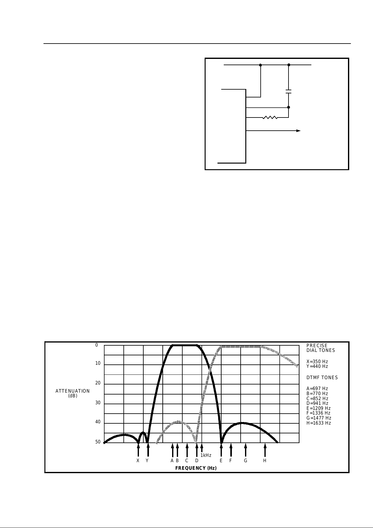
Figure 4 - B asic Steer ing Circ uit
providing tolerance to small frequency deviations
and variations. This averaging algorithm has been
developed to ensure an optimum combination of
immunity to talk-off and tolerance to the presence of
interfering frequencies (third tones) and noise. When
the detector recognizes the presence of two valid
tones (this is referred to as the “signal condition” in
some industry specifications) the “Early Steering”
(ESt) output will go to an active state. Any
subsequent loss of signal condition will cause ESt to
assume an in ac tive s ta te ( see “S te er in g Cir cu it”) .
Steering Circuit
Before registration of a decoded tone pair, the
receiver checks for a valid signal duration (referred
to as character recognition condition). This check is
performed by an external RC time constant driven by
ESt. A logic high on ESt caus es v
c
(see Figure 4) to
rise as the capacitor discharges. Provided signal
V
DD
C
v
c
V
DD
St/GT
ESt
StD
MT8870D/
MT8870D-1
R
t
GTA
=(RC)In(VDD/V
TSt
)
t
GTP
=(RC)In[VDD/(VDD-V
TSt
)]
Figure 3 - Filter Response
AA
AA
AA
AA
AA
AAAAAA
AA
AA
AA
AA
AA
A
AAA
AA
AA
AAAAAA
AAAAAA
AA
AA
AA
AA
AA
AA
AA
AA
AA
AA
AA
AA
AA
AA
AA
AAAAAA
AA
AA
AA
AA
AA
AAAAAAAAA
AA
AAA
AAAA
AAAA
AAAA
AAAA
AAAA
AAAAAAAAA
A
AAAA
AA
A
AA
AA
AA
AA
0
10
20
30
40
50
ATTENUATION
(dB)
XY ABCD
1kHz
EF G H
PRECISE
DIAL TONES
X=350 Hz
Y=440 Hz
DTMF TONES
A=697 Hz
B=770 Hz
C=852 Hz
D=941 Hz
E=1209 Hz
F=1336 Hz
G=1477 Hz
H=1633 Hz
FREQUENCY (Hz)
Page 4
MT8870D/MT8870D-1 ISO
2
-CMOS
4-14
condition is maintained (ESt remains high) for the
validation period (t
GTP
), vc reaches the threshold
(V
TSt
) of the steering logic to register the tone pair,
latching its corresponding 4-bit code (see Table 1)
into the output latch. At this point the GT output is
activated and drives v
c
to VDD. GT continues to drive
high as long as ESt remains high. Finally, after a
short delay to allow the output latch to settle, the
delayed steering output flag (StD) goes high,
signalling that a received tone pair has been
registered. The contents of the output latch are made
available on the 4-bit output bus by raising the three
state control input (TOE) to a logic high. The
steering circuit works in reverse to validate the
interdigit pause between signals. Thus, as well as
rejecting signals too short to be considered valid, the
receiver will tolerate signal interruptions (dropout)
too short to be considered a valid pause. This facility,
together with the capability of selecting the steering
time constants externally, allows the designer to
tailor performance to meet a wide variety of system
requirements.
Guard Time Adjustment
In many situations not requiring selection of tone
duration and interdigital pause, the simple steering
circuit shown in Figure 4 is applicable. Component
values are chosen according to the formula:
t
REC=tDP+tGTP
tID=tDA+t
GTA
The valu e of tDP is a device parameter (see Figure
11) and t
REC
is the minimum signal duration to be
recognized by the receiver. A value for C of 0.1 µF is
Figure 5 - Guard Time Adjustment
V
DD
St/GT
ESt
C
1
R
1
R
2
a) decreasing t
GTP
; (t
GTP<tGTA
)
t
GTP
=(RPC1)In[VDD/(VDD-V
TSt
)]
t
GTA
=(R1C1)In(VDD/V
TSt
)
R
P
=(R1R2)/(R1+R2)
V
DD
St/GT
ESt
C
1
R
1
R
2
t
GTP
=(R1C1)In[VDD/(VDD-V
TSt
)]
t
GTA
=(RPC1)In(VDD/V
TSt
)
R
P
=(R1R2)/(R1+R2)
b) decreasing t
GTA
; (t
GTP>tGTA
)
Table 1. Functional Decode Table
L=LOGIC LOW, H=LOGIC HIGH, Z=HIGH IMPEDANCE
X = DON‘T CARE
recommended for most applications, leaving R to be
selected by the designer.
Different steering arrangements may be used to
select independently the guard times for tone
present (t
GTP
) and tone absent (t
GTA
). This may be
necessary to meet system specifications which place
both accept and reject limits on both tone duration
and interdigital pause. Guard time adjustment also
allows the designer to tailor system parameters
such as talk off and noise immunity. Increasing t
REC
improves talk-off performance since it reduces the
probability that tones simulated by speech will
maintain signal condition long enough to be
registered. Alternatively, a relatively short t
REC
with
a long t
DO
would be appropriate for extremely noisy
environments where fast acquisition time and
immunity to tone drop-outs are required. Design
information for guard time adjustment is shown in
Figure 5.
Digit TOE INH ESt Q
4
Q
3
Q
2
Q
1
ANYLXHZZZZ
1HXH0001
2HXH0010
3HXH0011
4HXH0100
5HXH0101
6HXH0110
7HXH0111
8HXH1000
9HXH1001
0HXH1010
*HXH1011
#HXH1100
AHLH1101
BHLH1110
CHLH1111
DHLH0000
AHHL
undetected, the output code
will remain the same as the
previous detected code
BHHL
CHHL
DHHL
Page 5

ISO
2
-CMOS MT8870D/MT8870D-1
4-15
Power-down and Inhibit Mode
A logic high applied to pin 6 (PWDN) will power down
the device to minimize the power consumption in a
standby mode. It stops the oscillator and the
functions of the filters.
Inhibit mode is enabled by a logic high input to the
pin 5 (INH). It inhibits the detection of tones
representing characters A, B, C, and D. The output
code will remain the same as the previous detected
code (see Table 1).
Differential Input Configuration
The input arrangement of the MT8870D/MT8870D-1
provides a differential-input operational amplifier as
well as a bias source (V
Ref
) which is u se d to b ias th e
inputs at mid-rail. Provision is made for connection of
a feedback resistor to the op-amp output (GS) for
adjustment of gain. In a single-ended configuration,
the input pins are connected as shown in Figure 10
with the op-amp connected for unity gain and V
Ref
biasing the input at 1/2VDD. Figure 6 shows the
differential configuration, which permits the
adjustment of gain with the feedback resistor R
5
.
Crystal Oscillator
The internal clock circuit is completed with the
addition of an external 3.579545 MHz crystal and is
normally connected as shown in Figure 10 (SingleEnded Input Configuration). However, it is possible
to configure several MT8870D/MT8870D-1 devices
employing only a single oscillator crystal. The
oscillator output of the first device in the chain is
coupled through a 30 pF capacitor to the oscillator
input (OSC1) of the next device. Subsequent devices
are connected in a similar fashion. Refer to Figure 7
for details. The problems associated with
unbalanced loading are not a concern with the
arrangement shown, i.e., precision balancing
capacitors are not required.
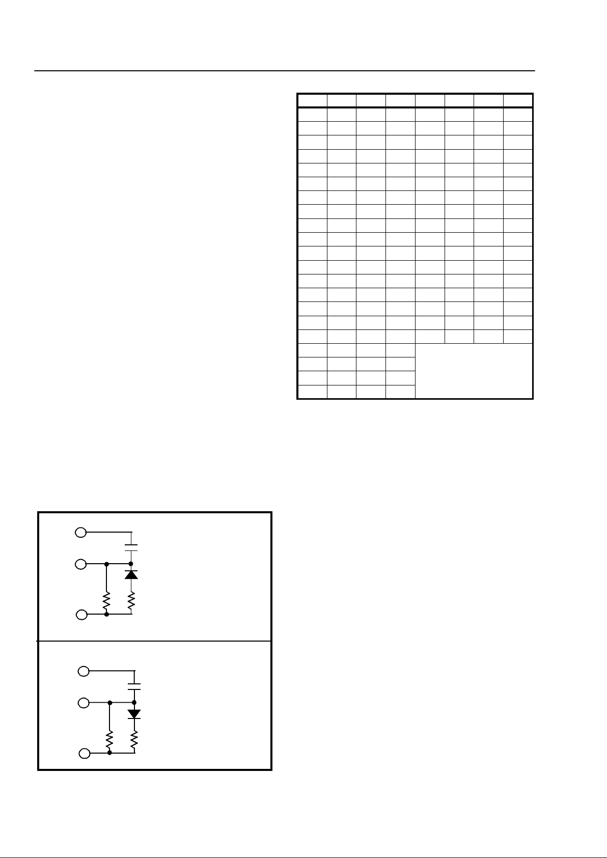
Figure 6 - Differential Input Configuration
Figure 7 - Oscillator Connection
Table 2. Recommended Resonator Specifications
Note: Qm= qu al ity factor of R L C m od el , i .e. , 1 / 2ΠƒR1C1.
Parameter Unit Resonator
R1 Ohms 10.752
L1 mH .432
C1 pF 4.984
C0 pF 37.915
Qm - 896.37
∆f % ±0.2%
C1R
1
C
2
R
4
R
3
IN+
IN-
+
-
R
5
GS
R
2
V
Ref
MT8870D/
MT8870D-1
Differential Input Amplifier
C1=C2=10 nF
R
1=R4=R5
=100 kΩ
R
2
=60kΩ, R3=37.5 kΩ
All resistors are ±1% tolerance.
All capacitors are ±5% tolerance.
R
3
=
R
2R5
R2+R
5
VOLTAGE GAIN (Av diff)=
R
5
R
1
INPUT IMPEDANCE
(Z
INDIFF
) = 2
R
1
2
+
1
ωc
2
OSC1
OSC2
OSC2
OSC1
C
X-tal
C
To OSC1 of next
MT8870D/MT8870D-1
C=30 pF
X-tal=3.579545 MHz
Page 6

MT8870D/MT8870D-1 ISO
2
-CMOS
4-16
Applications
RECEIVER SYS TEM F OR BRITISH TELECOM
SPEC POR 1151
The circuit shown in Fig. 9 illustrates the use of
MT8870D-1 device in a typical receiver system. BT
Spec defines the input signals less than -34 dBm as
the non-operate level. This condition can be
attained by choosing a suitable values of R
1
and R
2
to provide 3 dB attenuation, such that -34 dBm input
signal will correspond to -37 dBm at the gain setting
pin GS of MT8870D-1. As shown in the diagram, the
component values of R
3
and C2 are the guard time
requirements when the total component tolerance is
6%. For better performance, it is recommended to
use the non-symmetric guard time circuit in Fig. 8.
Figure 8 - Non-Symmetric Guard Time Circuit
t
GTP
=(RPC1)In[VDD/(VDD-V
TSt
)]
t
GTA
=(R1C1)In(VDD/V
TSt
)
R
P
=(R1R2)/(R1+R2)
V
DD
St/GT
ESt
C
1
R
2
R
1
Notes:
R1=368K Ω ± 1%
R
2
=2.2M Ω ± 1%
C
1
=100nF ± 5%
Figure 9 - Single-Ended Input Configuration for BT or CEPT Spec
IN+
INGS
V
Ref
INH
PWDN
OSC 1
OSC 2
V
SS
TOE
V
DD
St/GT
ESt
StD
Q4
Q3
Q2
Q1
DTMF
Input
C
1
R
1
R
2
X
1
V
DD
C
2
R
3
MT8870D-1
NOTES:
R
1
= 102KΩ ± 1%
R
2
= 71.5KΩ ± 1%
R
3
= 390KΩ ±1 %
C
1,C2
= 100 nF ± 5%
X
1
= 3.579545 MHz ± 0.1%
V
DD
= 5.0V ± 5%
Page 7

ISO
2
-CMOS MT8870D/MT8870D-1
4-17
† Exceeding these values may cause permanent damage. Functional operation under these conditions is not implied.
Derate ab o ve 75 °C at 16 m W / °C. All le ad s s old ered to bo a rd.
‡ Typical figures are at 25°C and are for design aid only: not guaranteed and not subject to producti on testing.
‡ Typical figures are at 25°C and are for design aid only: not guaranteed and not subject to producti on testing.
Absolute Maximum Ratings
†
Parameter Symbol Min Max Units
1 DC Power Supply Voltage V
DD
7V
2 Voltage on any pin V
I
VSS-0.3 VDD+0.3 V
3 Current at any pin (other than supply) I
I
10 mA
4 Storage temperature T
STG
-65 +150 °C
5 Package power dissipation P
D
500 mW
Recommended Operating Conditions - Voltages are with respect to ground (V
SS
) unless otherwise stated .
Parameter Sym Min Typ
‡
Max Units Test Conditions
1 DC Power Supply Voltage V
DD
4.75 5.0 5.25 V
2 Operating Tem perat u re T
O
-40 +85 °C
3 Crystal/Clock Frequency fc
3.579545
MHz
4 Crystal/Clock Freq.Tolerance ∆fc ±0.1 %
DC Electrical Characteristics - V
DD
=5.0V± 5%, VSS=0V, -40°C ≤ TO ≤ +85°C, unless otherwise stated.
Characteristics Sym Min Typ
‡
Max Units Test Conditions
1
S
U
P
P
L
Y
Standby supply current I
DDQ
10 25 µA PWDN=V
DD
2 Operating supply current I
DD
3.0 9.0 mA
3 Power consumption P
O
15 mW fc=3.579545 MHz
4
I
N
P
U
T
S
High level input V
IH
3.5 V VDD=5.0V
5 Low level input voltage V
IL
1.5 V VDD=5.0V
6 Input leakage current I
IH/IIL
0.1 µAVIN=V
SS
or V
DD
7 Pull up (source) current I
SO
7.5 20 µA TOE (pin 10)=0,
V
DD
=5.0V
8 Pull down (sink) current I
SI
15 45 µA INH=5.0V, PWDN=5.0V,
V
DD
=5.0V
9 Input impedance (IN+, IN-) R
IN
10 MΩ @ 1 kHz
10 Steering threshold voltage V
TSt
2.2 2. 4 2 .5 V VDD = 5.0V
11
O
U
T
P
U
T
S
Low level output voltage V
OL
VSS+0.03 V No load
12 High level output voltage V
OHVDD
-0.03 V No load
13 Output low (sink) current I
OL
1.0 2.5 mA V
OUT
=0.4 V
14 Output high (source) current I
OH
0.4 0.8 mA V
OUT
=4.6 V
15 V
Ref
output voltage V
Ref
2.3 2.5 2.7 V No load, VDD = 5.0V
16 V
Ref
output resistance R
OR
1kΩ
Page 8

MT8870D/MT8870D-1 ISO
2
-CMOS
4-18
‡ Typical figures are at 25 °C and are for design aid only: not guaranteed and not subject to produ ctio n testin g.
*NOTES
1. dBm= decibel s abov e or belo w a refer enc e power of 1 mW into a 600 ohm lo ad.
2. Digit sequence consists of all DTMF tones.
3. Tone duration= 4 0 m s , ton e pa us e= 4 0 m s .
4. Sign al c on dit ion consis ts o f n om in al D TM F frequencies .
5. Both to ne s in composi te si gn al have an equal amplitude.
6. Tone pair is d eviated by ±1 .5 %± 2 Hz.
7. Band w id th li mited (3 k Hz ) Ga us si an noise.
8. The precise dial tone frequencies are (350 Hz and 440 Hz) ± 2 %.
9. For a n err o r ra te of better t ha n 1 i n 1 0, 00 0.
10. Refe ren ce d to lowest level freque nc y co m po ne nt in D TM F si gn al .
11. Re fe r en c ed to th e minimum v ali d accept le v el.
12. Guaranteed by design and characterization.
Operating Characteristics - V
DD
=5.0V±5%, VSS=0V, -40°C ≤ TO ≤ +85°C ,unless otherwise stated.
Gain Setting Amplifier
Characteristics Sym Min Typ
‡
Max Units Test Conditions
1 Input leakage current I
IN
100 nA V
SS
≤ VIN ≤ V
DD
2 Input resistance R
IN
10 MΩ
3 Input offset voltage V
OS
25 m V
4 Power supply rejection PSRR 50 dB 1 kHz
5 Common mode rejection CMRR 40 dB 0.75 V ≤ V
IN
≤ 4.25 V biased
at V
Ref
=2.5 V
6 DC open loop voltage gain A
VOL
32 dB
7 Unity gain bandwidth f
C
0.30 MHz
8 Output voltage swing V
O
4.0 V
pp
Load ≥ 100 kΩ to V
SS
@ GS
9 Maximum capacitive load (GS) C
L
100 pF
10 R e sistive load (GS) R
L
50 kΩ
11 Common mode range V
CM
2.5 V
pp
No Load
MT8870D AC Electrical Characteristics -V
DD
=5.0V ±5%, VSS=0V, -40°C ≤ TO ≤ +85°C , using Test Circuit shown in
Figure 10.
Characteristics Sym Min Typ‡Max Units Notes*
1
V alid input signal levels (each
tone of composite signal)
-29 +1 dBm 1,2,3,5,6, 9
27.5 869 mV
RMS
1,2,3,5, 6, 9
2 Negative twist accept 8 dB 2,3,6,9,12
3 Positive twist accept 8 dB 2,3,6,9, 12
4 Frequency deviat ion ac cept ±1.5% ± 2 Hz 2,3,5,9
5 Frequency deviation reject ±3.5% 2,3,5,9
6 Third tone tolerance -16 dB 2,3,4,5, 9,10
7 Noise tolerance -12 dB 2,3,4,5,7,9,10
8 Dial tone tolerance +22 dB 2,3,4,5,8,9,11
Page 9

ISO
2
-CMOS MT8870D/MT8870D-1
4-19
‡ Typical figures are at 25 °C and are for design aid only: not guaranteed and not subject to produ ctio n testing.
*NOTES
1. dBm= decibels above or below a reference power of 1 mW into a 600 ohm load.
2. Digit se qu en c e c o ns is ts of a ll D TM F t on es .
3. Tone duration= 40 m s, t on e p au s e= 40 ms.
4. Signa l co nd iti on c on s is ts of no m in al D TM F fr eq ue n ci es .
5. Both ton es i n c o mp os ite signal have an equal amplitude.
6. Tone pair is de viated by ±1 .5 %± 2 Hz .
7. Band w id th lim i ted (3 kHz ) G au s si an noise.
8. The p re ci se d ia l to ne freque nc ie s ar e (3 50 H z a nd 44 0 Hz) ± 2 %.
9. For a n e rro r ra te of better than 1 in 10,0 00 .
10. Refe ren ce d to lowest level freque nc y co m po ne nt in D TM F si gn al .
11. Re fe r en c ed to th e minimum v ali d accept le v el.
12. Referenced to Fig. 10 input DTMF tone level at -25dBm (-28dBm at GS Pin) interference frequency range between 480-3400Hz.
13. Guaranteed by design and characterization.
MT8870D-1 AC Electrical Characteristics -V
DD
=5.0V±5%, VSS=0V, -40°C ≤ TO ≤ +85°C , using Test Circuit shown in
Figure 10.
Characteristics Sym Min Typ
‡
Max Units Notes*
1
V alid input signal levels (each
tone of composite signal)
-31 +1 dBm T ested at V
DD
=5.0V
1,2,3,5,6,9
21.8 869 mV
RMS
2 Input Signal Level Reject
-37 dBm T ested at V
DD
=5.0V
1,2,3,5,6,9
10.9 mV
RMS
3 Negative twist accept 8 dB 2,3,6,9,13
4 Positive twist acce p t 8 dB 2,3,6,9,13
5 Frequency deviation accept ±1.5%± 2 Hz 2,3,5,9
6 Frequency deviation reject ± 3.5% 2,3,5,9
7 Third zone tolerance -18.5 dB 2,3,4,5,9,12
8 Noise tolerance -12 dB 2,3,4,5,7,9,10
9 Dial tone tolerance +22 dB 2,3,4,5,8,9,11
Page 10

MT8870D/MT8870D-1 ISO
2
-CMOS
4-20
‡ Typical figures are at 25°C and are for design aid only: not guaranteed and not subject to producti on testing.
*NOTES:
1. Used for g ua rd- t im e c a lc ul ati on p ur p os e s only.
2. These, use r a djustable paramete rs , a r e no t d ev ic e sp ec if ic ations. T he a dj us tab le settin gs of these m in im um s a nd m ax im u ms
are recommendations based upon network requirements.
3. With valid ton e present at in pu t, t
PU
equals time from P D WN g oi ng l ow u nt il E St going hig h.
Figure 10 - Single-Ended Input Configuration
AC Electrical Characteristics - V
DD
=5.0V±5%, VSS=0V, -40°C ≤ To ≤ +85°C , using Test Circuit shown in Figure 10.
Characteristics Sym Min Typ
‡
Max Units Conditions
1
T
I
M
I
N
G
Tone present det ect time t
DP
5 11 14 ms Note 1
2 Tone absent detect time t
DA
0.5 4 8.5 ms Note 1
3 Tone durat ion a ccep t t
REC
40 ms Note 2
4 Tone durat ion reject t
REC
20 ms Note 2
5 Interdigit pause accept t
ID
40 ms Note 2
6 Interdigit pause reject t
DO
20 ms Note 2
7
O
U
T
P
U
T
S
Propagation delay (St to Q) t
PQ
811µsTOE=V
DD
8 Propagation delay (St to StD) t
PStD
12 16 µsTOE=V
DD
9 Output data set up (Q to StD) t
QStD
3.4 µsTOE=V
DD
10 Propagati on delay (TOE to Q ENABLE) t
PTE
50 ns load of 10 kΩ,
50 pF
11 Propagation delay (TOE to Q DISAB LE) t
PTD
300 ns load of 10 kΩ,
50 pF
12
P
D
W
N
Power-up time t
PU
30 ms Note 3
13 Power-down time t
PD
20 ms
14
C
L
O
C
K
Crystal/clock frequency f
C
3.5759 3.5795 3.5831 MHz
15 Clock input rise ti me t
LHCL
110 ns Ext. clock
16 Clock input fall time t
HLCL
110 ns Ext. clock
17 Clock in put duty cycle DC
CL
40 50 60 % Ext. clock
18 Capacitive load (OSC 2) C
LO
30 pF
IN+
INGS
V
Ref
INH
PDWN
OSC 1
OSC 2
V
SS
TOE
V
DD
St/GT
ESt
StD
Q4
Q3
Q2
Q1
DTMF
Input
C
1
R
1
R
2
X-tal
V
DD
C
2
R
3
NOTES:
R
1,R2
=100KΩ ± 1%
R
3
=300 KΩ ± 1%
C
1,C2
=100 nF ± 5%
X-tal=3.579545 MHz ± 0.1%
MT8870D/MT8870D-1
Page 11

ISO
2
-CMOS MT8870D/MT8870D-1
4-21
Figure 11 - Timing Diagram
V
in
ESt
St/GT
Q
1-Q4
StD
TOE
EVENTS
ABC
D
EFG
t
REC
t
REC
t
ID
t
DO
TONE #n
TONE
#n + 1
TONE
#n + 1
t
DP
t
DA
t
GTP
t
GTA
t
PQ
t
QStD
t
PSrD
t
PTD
t
PTE
# n # (n + 1)
HIGH IMPEDANCE
DECODED TONE # (n-1)
EXPLANATION OF EVENTS
EXPLANATION OF SYMBOLS
A) TONE BURSTS DETECTED, TONE DURATION INVALID, OUTPUTS NOT UPDATED.
B) TONE #n DETECTED, TONE DURATION VALID, TONE DECODED AND LATCHED IN OUTPUTS
C) END OF TONE #n DETECTED, TONE ABSENT DURATION VALID, OUTPUTS REMIAN LATCHED UNTIL NEXT VALID
TONE.
D) OUTPUTS SWITCHED TO HIGH IMPEDANCE STATE.
E) TONE #n + 1 DETECTED, TONE DURATION VALID, TONE DECODED AND LATCHED IN OUTPUTS (CURRENTLY
HIGH IMPEDAN CE).
F) ACCEPTABLE DROPOUT OF TONE #n + 1, TONE ABSENT DURATION INVALID, OUTPUTS REMAIN LATCHED.
G) END OF TONE #n + 1 DETECTED, TONE ABSENT DURATION VALID, OUTPUTS REMAIN LATCHED UNTIL NEXT
VALID TONE.
V
in
DTMF COMPOSITE INPUT SIGNAL.
ESt EARLY STEERING OUTPUT. INDICATES DETECTION OF VALID TONE FREQUENCIES.
St/GT STEERING INPUT/GUARD TIME OUTPUT. DRIVES EXTERNAL RC TIMING CIRCUIT.
Q
1-Q4
4-BIT DECODED TONE OUTPUT.
StD DELAYED STEERING OUTPUT. INDICATES THAT VALID FREQUENCIES HAVE BEEN PRESENT/ABSENT FOR THE
REQUIRED GUARD TIME THUS CONSTITUTING A VALID SIGNAL.
TOE TONE OUTPUT ENABLE (INPUT). A LOW LEVEL SHIFTS Q
1-Q4
TO ITS HIGH IMPEDANCE STATE.
t
REC
MAXIMUM DTMF SIGNAL DURATION NOT DETECED AS VALID
t
REC
MINIMUM DTMF SIGNAL DURATION REQUIRED FOR VALID RECOGNITION
t
ID
MAXIMUM TIME BETWEEN VALID DTMF SIGNALS.
t
DO
MAXIMUM ALLOWAB L E DROP OUT D U R I NG VALID D TM F SI GN AL.
t
DP
TIME TO DETECT THE PRESENCE OF VALID DTMF SIGNALS.
t
DA
TIME TO DETECT THE ABSENCE OF VALID DTMF SIGNALS.
t
GTP
GUARD TIME, TONE PRESENT.
t
GTA
GUARD TIME, TONE ABSENT.
V
TSt
Page 12

MT8870D/MT8870D-1 ISO
2
-CMOS
4-22
NOTES:
 Loading...