

Page 1
2-265
Features
• Loop Start Trunk Interface
• 600Ω & 900Ω Input Impedance
• 2-4 Wire Conversion
• Line state Detection Outputs:
• - Forward Loop
• - Reverse Loop
• - Ringing Voltage
• - Switch Hook
• One Relay Driver
• On-Hook Reception
• Small footprint area
• Meets FCC Part 68 Leakage Current
Requirements
Applications
Interface to Central Office for:
• PABX
• Key Telephone Systems
• Channel Bank
• Voice Mail
• Ter minal Equipment
• Digital Loop Carrier
• Optical Multiplexer
Description
The Mitel MH88634-2 Central Office Interface Circuit
trunk provides a complete analogue and signalling
link between audio switching equipment and a
telephone Line. The device is available in a single in
line package for high packing densities or with a lead
frame formed at 90° for low clearance applications.
The device is fabricated as a thick film hybrid
incorporating various technologies for optimum
circuit design and very high reliability.
This part supercedes the MH88634-2 and is pin for pin
compatible.
We advise that the B rev parts are fully tested.
However, we do not expect to see changes between
MH88634-2 and MH88634BV-2.
The component design has been changed to
improve the general performance of the part. It is
also now capable of operating at a 24V battery.
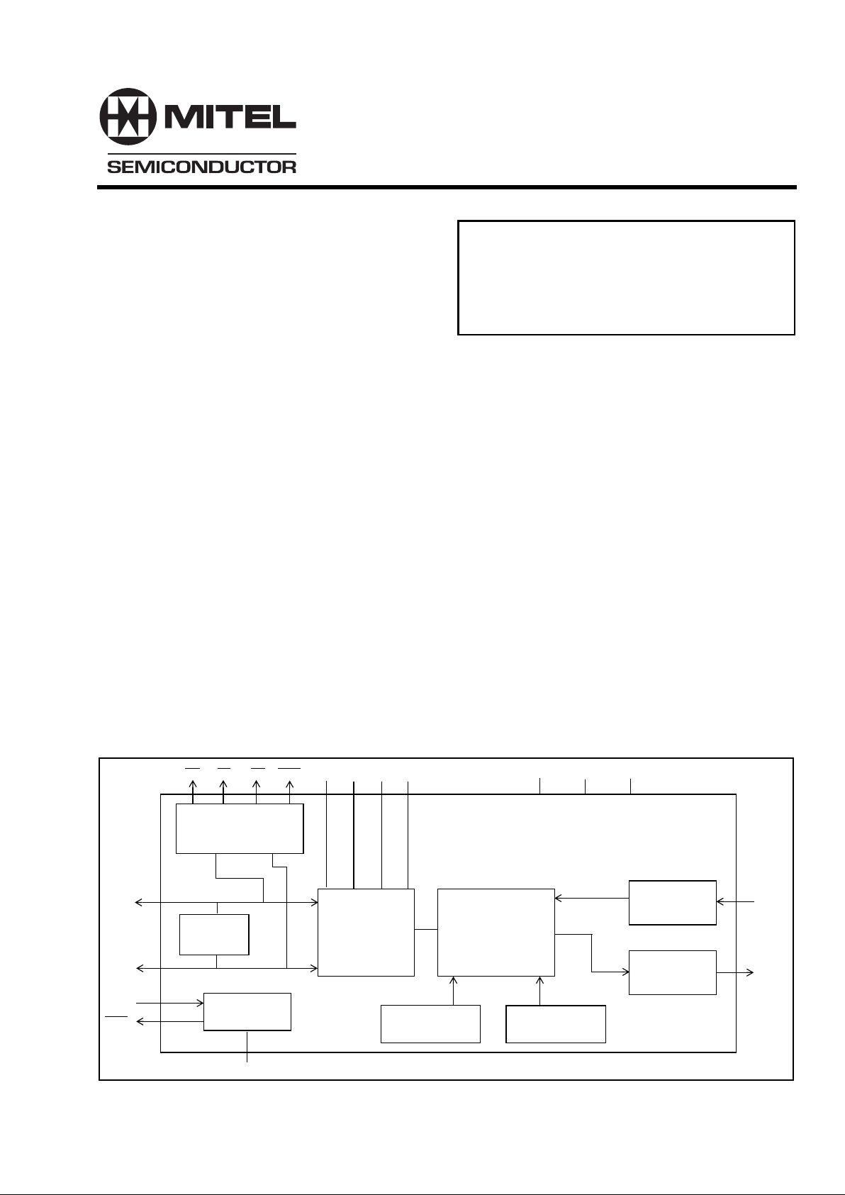
Figure 1 - Functional Block Diagram
Status
Detection
Receive
Gain
Transmit
Gain
2 - 4 Wire
Hybrid
Dummy
Ringer
Line
Termination
Loop Relay
Driver
Impedance
Matching
Network
Balance
XLA XLB XLC
XLD
LRC
LRD
VRLY
RING
TIP
RV
VCC
RX
TX
VEE AGND
FL RL
SHK
DS5061 ISSUE 6 January 1999
Ordering Information
MH88634BV-2 21 Pin SIL Package
MH88634BT-2 21 Pin 90° L/F Package
MH88634BV-4 21 Pin SIL Package
0°C to 70°C
MH88634B
Central Office Interface Circuit
Advance Information
Page 2
MH88634B Advance Information
2-266
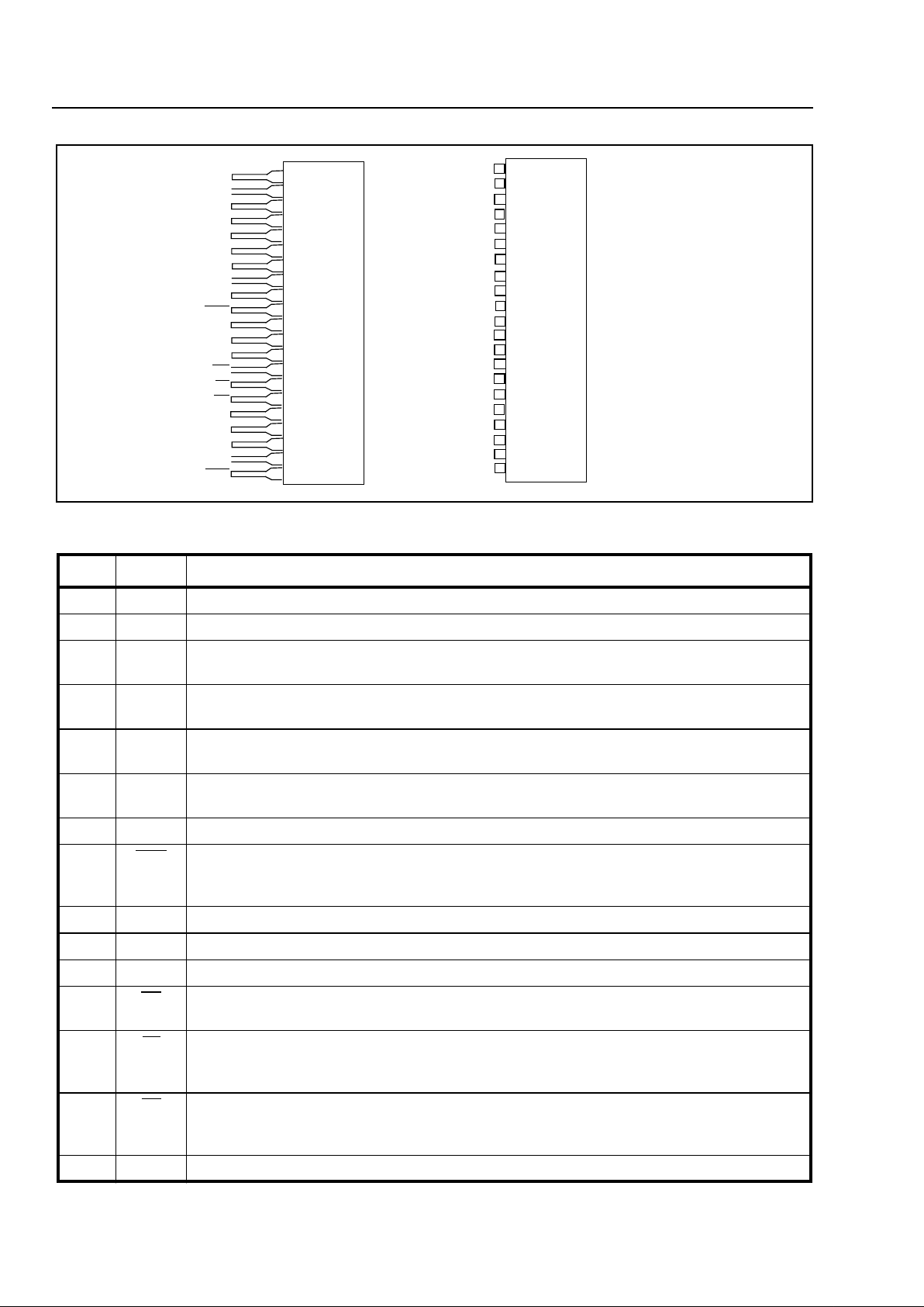
Figure 2 - Pin Connections
Pin Description
Pin # Name Description
1 TIP Tip Lead. Connects to the "Tip" lead of a Telephone Line.
2 RING Ring Lead. Connects to the "Ring" lead of a Telephone Line.
3 XLA Loop Relay Contact A. Connects to XLB through the Loop relay (K1) contacts when the
relay is activated.
4 XLD Loop Relay Contact D. Connects to XLC through the loop relay (K1) contacts, when the
relay is activated.
5 XLB Loop Relay Contact B. Connects to XLA through the loop relay (K1) contacts, when the
relay is activated.
6 XLC Loop Relay Contact C. Connects to XLD through the loop relay (K1) contacts, when the
relay is activated.
7-9 IC Internal Connection. No connection should be made to this pin.
10 SHK Switch Hook (Output). A logic 0 indicates the presence of forward or reverse battery
voltage when LRC is logic 0 and the presence of forward or reverse loop current when LRC
is logic 1.
11 RX Receive (Input). 4-Wire ground (AGND) referenced analog input.
12 VEE Negative Supply Voltage. -5V DC
13 TX Transmit (Output). 4-Wire ground (AGND) referenced analog output.
14 RV Ringing Voltage Detect (Output). A logic low indicates that ringing voltage is across the Tip
and Ring leads.
15 FL Forward Loop Detect (Output). In the on-hook state, a logic 0 output indicates that
forward loop battery is present. In the off-hook state, a logic 0 indicates that forward loop
current is present.
16 RL Reverse Loop Detect (Output). In the on-hook state, a logic 0 output indicates that
reverse loop battery is present. In the off-hook state, a logic 0 output indicates that reverse
loop current is present.
17 VCC Positive Supply Voltage. +5V DC
1
2
3
4
5
6
7
8
9
10
11
12
13
14
15
16
17
18
19
20
TIP
RING
XLA
XLB
XLC
IC
IC
IC
RX
VEE
TX
RV
FL
RL
VCC
AGND
LRC
VRLY
LRD
21
XLD
SHK
21
20
19
18
17
16
15
14
13
12
11
10
9
8
6
5
4
3
2
1
7
Page 3

Advance Information MH88634B
2-267
18 AGND Analog Ground. 4-wire ground (AGND). Normally connected to system ground.
19 LRC Loop Relay Control (Input). A logic 1 activates the Loop Relay Driver output (LRD).
20 VRLY Relay Positive Supply Voltage. Typically +5V. Connects to the relay supply voltage.
21 LRD Loop Relay Drive (Output). Connects to the Loop Relay Coil. When LRC is at a logic 1 an
open collector output at LRD sinks current and energizes the relay.
Pin Description (continued)
Functional Description
The MH88634 is a Central Office Interface Circuit
(COIC). It is used to correctly terminate a Central
Office 2-wire telephone line. The device provides a
signalling link and a 2-4 Wire line interface between
the Telephone Line and subscr iber equipment. The
subscriber equipment can include Private Branch
Exchanges (PBXs), Key Telephone Systems,
Terminal Equipment, Digital Loop Carriers and
Wireless Local Loops.
All descriptions assume that the device is connected
as in the application circuit shown in Figure 3.
Isolation Barrier
The MH88634 provides an isolation barrier which is
designed to meet FCC Part 68 (November 1987)
Leakage Current Requirements.
External Protection Circuit
An external Protection Circuit Device assists in
preventing damage to the device and the
subscriber’s equipment, due to over-voltage
conditions. The type of protection required is
dependant upon the application and regulatorary
standards. Further details should be obtained from
the specific country’s regulatorary body. Typically
you will need lightening protection supplied by
resettable fuses or PTCTM and mains crossover
protection via a foldover diode.
Suitable Markets
The MH88634BV-2/BT-2 has fixed 600Ω line and
network balance impedance for use in North
America and Asia.
The MH88634BV-4 has a fixed 900R impedance and
is also suitable for some applications in North and
South America
Line Termination
When LRC is at a logic 1, LRD will sink current
which energizes the Loop Relay (K1), connecting
XLA to XLB and XLC to XLD. This places a line
termination across Tip and Ring. The device can be
considered to be in an off-hook state and DC loop
current will flow. The line termination consists of a
DC resistance and an AC impedance. When LRC is
at a logic 0, the line termination is removed from
across Tip and Ring.
An internal Dummy Ringer is permanently connected
across Tip and Ring which is a series AC load of
(17kΩ+330nF). This represents a mechanical
telephone ringer and allows ringing voltages to be
sensed. This load can be considered negligible
when the line has been terminated.
Depending on the Network Protocol being used the
Line Termination can terminate an incoming call,
seize the line for an outgoing call, or if applied and
disconnected at the correct rate can be used to
generate dial pulse signals.
The DC line termination circuitry provides the line
with an active DC load termination which is
equivalent to a DC resistance of 280Ω at 20mA
Ringing Equivalent Number
The Ringing Equivalent Number (REN) is application
specific. See the governing regulatory body
specification for details.
Input Impedance
The input impedance (Zin) is the AC impedance that
the MH88634 places across Tip and Ring to
terminate the Telephone line. This is fixed at 600Ω
on the -2 variant and 900R on the -4.
Page 4

MH88634B Advance Information
2-268
Network Balance Impedance
The MH88634BV-2/BT-2’s Network Balance
Impedance is fixed at 600Ω.
The MH88634BV-4 Network Balance Impedance is
fixed at 900R.
2-4 Wire Conversion
The device converts the balanced 2-Wire input,
presented by the line at Tip and Ring, to a ground
referenced signal at TX. This circuit operates with or
without loop current; signal reception with no loop
current is required for on-hook reception enabling the
detection of Caller Line Identification (CLI) signals.
Conversely the device converts the ground
referenced signal input at RX, to a balanced 2-Wire
signal across Tip and Ring.
The 4-Wire side (TX and RX) can be interfaced to a
filter/codec, such as the Mitel MT896X, for use in
digital voice switched systems
During full duplex transmission, the signal at Tip and
Ring consists of both the signal from the device to
the line and the signal from the line to the device.
The signal input at RX, being sent to the line, must
not appear at the output TX. In order to prevent this,
the device has an internal cancellation circuit. The
measure of attenuation is Transhybrid Loss (THL).
Transmit and Receive Gain
The Transmit Gain of the device is the gain from the
balanced signal across Tip and Ring to the ground
referenced signal at TX. It is set at 0dB.
The Receive Gain of the device is the gain from the
ground referenced signal at RX to the balanced
signal across Tip and Ring. It is set at -2dB.
Supervision Features
Line Status Detection Outputs
The MH88634 supervisory circuitry provides the
signalling status outputs which are monitored by the
system controller. The supervisory circuitry is
capable of detecting: Ringing Voltage; Forward and
Reverse loop battery; Forward and Reverse loop
current; and Switch Hook.
Ringing Voltage Detect Output (RV)
The RV output provides a logic 0 when ringing
voltage is detected across Tip and Ring. This
detector includes a filter which ensures that the
output toggles at the ringing cadence and not at the
ringing frequency. Typically this output switches to a
logic 0 after 50ms of applied ringing voltage and
remains at a logic 0 for 50ms after ringing voltage is
removed.
The threshold is different on the two variants. The
900R part has been designed to meet the ring
sensitivity requirements of TR57, 30 not detecting
ringin below 35Vrms.
Forward Loop and Reverse Loop Detect Outputs
(FL & RL)
The FL output provides a logic 0 when either forward
loop battery or forward loop current is detected, that
is the Ring pin voltage is more negative than the Tip
pin voltage.
The RL output provides a logic 0 when either reverse
loop battery or reverse loop current is detected, that
is the Tip pin voltage is more negative than the Ring
pin voltage.
Switch Hook (SHK)
The SHK output is active if either forward loop or
reverse loop current is detected, or if forward or
reverse battery voltage is detected.
Control Input
The MH88634 accepts a control signal from the
system controller at the Loop Relay Control input
(LRC). This energises the relay drive output Loop
Relay Drive (LRD). The output is active low and has
an internal clamp diode to VRLY.
The intended use of this relay driver is to add and
remove the Line Termination from across Tip and
Ring, as shown in Figure 3.
If this Control input and the Supervisory Features are
used as indicated in Figure 3, Loop-Start Signalling
can be implemented.
Mechanical Data
See Figure 9 for details of the mechanical
specification.
Page 5

Advance Information MH88634B
2-269
Figure 3 - Typical LS Application Circuit
MH88634
Analog Out
Analog In
Ringing Detect
Forward Loop
Reverse Loop
Switch Hook
-5V
+5V
K1
Protection
Circuit
Tip
Ring
Loop Relay Control
TIP
RING
LRD
VRLY
LRC
XLA
XLB
XLC
XLD
VCC
AGND
VEE
SHK
RL
FL
RV
RX
TX
K1
NOTES:
1) K1 Electro Mechanical 2 Form A
K1
C1
C2
2) C1 and C2 are decoupling capacitors
5
3
15
16
6
10
4
18
12
14
19
21
2
20
11
13
17
1
+5V
Page 6

MH88634B Advance Information
2-270
*Exceeding these values may cause permanent damage. Functional operation under these conditions is not implied.
‡ Typical figures are at 25°C with nominal 5V supplies and are for design aid only.
s
† Electrical Characteristics are over recommended operating conditions unless otherwise stated.
‡ Typical figures are at 25°C with nominal 5V supplies and are for design aid only.
Absolute Maximum Ratings*
Parameters Sym Min Max Units Comments
1 DC Supply Voltages V
CC
V
EE
-0.3
0.3
7
-7
V
V
2 DC Ring Relay Voltage V
RLY
-0.3 18 V
3 Storage Temperature
T
S
-55 +125 ˚C
4 Ring Trip Current I
TRIP
180 mArms 250ms 10% duty cycle or 500ms single shot
Recommended Operating Conditions
Parameters Sym Min Typ
‡
Max Units
1 DC Supply Voltages V
CC
V
EE
4.75
-4.75
5.0
-5.0
5.25
-5.25
V
V
2 DC Ring Relay Voltage V
RLY
5.0 15 V
3 Operating Temperature T
OP
02570˚C
DC Electrical Characteristics
†
Characteristics Sym Min Typ
‡
Max Units Test Conditions
1 Supply Current I
CC
I
EE
5
2.5
13
13
mA
mA
2 Power Consumption PC 37.5 137 mW V
BAT
not connected
3 FL
RL
SHK
RV
Low Level Output Voltage
High Level Output Voltage
V
OL
V
OH
2.4
0.5 V
V
IOL = 4mA
IOH= 0.4mA
4 LRD Sink Current, Relay to
V
CC
Clamp Diode Current
I
OL
I
CD
100
150
mAmAVOL = 0.35V not
continuous, LRC=5V
5 LRC Low Level Input Voltage
High Level Input Voltage
V
IL
V
IH
2.0
0.8 V
V
6 LRC High Level Input Current
Low Level Input Current
I
IH
I
IL
40
40
µAµAVIH = 5.0V
Page 7

Advance Information MH88634B
2-271
† Electrical Characteristics are over recommended operating conditions unless otherwise stated.
‡ Typical figures are at 25°C with nominal 5V supplies and are for design aid only.
Note 1: Maximum figure of 282Ω at 0°C
DC Electrical Characteristics
†
Characteristics Symbol Min Typ
‡
Max Units Test Conditions
1 Ringing Voltage VR 40 90 150 V
rms
-2 Variant only
17 to 68Hz
2 Detect
No Detect
VR 60 106
35
V
rms
-4 Variant only
-4 Variant only
16-33Hz
(TR57 compliant)
3 Operating Loop Current 16 70 mA
4 Off-Hook DC Resistance 270 280 Ω @ 20mA Note 1
5 Leakage Current
(Tip-Ring to AGND)
7 mArms @ 1000VAC
6 SHK & FL Threshold
Tip-Ring (On-hook)
Tip-Ring Current (Off-Hook)
12
5
21
15
VdcmALRC = 0V
LRC = 5V
7 SHK & RL Threshold
Tip-Ring (On-Hook)
Tip-Ring Current (Off-Hook)
12
-5
21
-15
VdcmALRC = 0V
LRC = 5V
Page 8

MH88634B Advance Information
2-272
† Electrical Characteristics are over recommended operating conditions unless otherwise stated.
‡ Typical figures are at 25°C with nominal 5V supplies and are for design aid only.
AC Electrical Characteristics
†
Characteristics Symbol Min Typ
‡
Max Units Test Conditions
1 2-wire Input Impedance Zin 600
900
Ω -2 Variant
-4 Variant
2 Return Loss at 2-wire RL
20 29 dB
Test Circuit as Fig 6
200-3400 Hz
3 Longitudinal to Metallic
Balance 58
55
53
60
60
58
dB
dB
dB
Test Circuit as Fig 7
200Hz
1000Hz
3400Hz
4 Transhybrid Loss THL 20 27 dB 200-3400Hz
5 Gain, 2 wire to TX
Relative Gain
-0.25
-0.3
0
0
0.25
0.3
dB
dB
Test Circuit as Fig 4
1000Hz
200-3400Hz
6 Gain, Rx to 2 wire
Relative Gain
-2.25
-0.3
-2
0
-1.75
0.3
dB
dB
Test Circuit as Fig 5
1000Hz
200-3400Hz
7 Input impedance at RX 10 kΩ
8 Output impedance at TX 5 Ω
9 Signal Overload Level
at 2-wire
at TX
4.0
1.7
dBm
dBm
% THD < 5% @ 20mA
10 Total Harmonic Distortion
at 2-wire
at TX
THD
1.0
1.0
%
%
Input 0.5V, 1kHz @
RX
Input 0.5V, 1kHz @
Tip-Ring
11 Idle Channel Noise
at 2-Wire
at TX
NC
15
15
16.5
16.5
dBrnC
dBrnC
12 Power Supply Rejection Ratio
at 2-wire and TX
V
CC
V
EE
PSRR
25
25
48
47
dB
dB
Ripple 0.1V, 1kHz
13 On-Hook Gain, 2-Wire to TX
Relative to Off-Hook Gain
-1 0 1 dB Input 1000Hz @ 0.5V
14 Met. to Long. Balance
-2 Variant
-4 Variant
60
40
55
40
62
48
62
48
Test Circuit as Fig. 8
200-1000Hz
1000-3400Hz
200-1000Hz
1000-3400Hz
15 Common Mode Rejection
Ratio
CMRR 48 55 dB Test Circuit as Fig. 7
1000Hz, FL = 0V,
I
Loop
= 25mA
Page 9

Advance Information MH88634B
2-273
Figure 4 - 2-4 Wire Gain Test Circuit
Figure 5 - 4-2 Wire Gain Test Circuit
~
100uF
RING
TIP
XLA
XLB
XLC
XLD
Vs = 0.5V
600
Ω
AGND
VCC
VEE
RX
TX
100uF
+5V
-5V
I = 25mA
10H 300Ω
10H 300Ω
+
+
Gain = 20 * Log (Vtx/Vs)
-V
V
tx
V
~
Vs = 0.5V
Z = 600Ω
Gain = 20 * Log (Vz/Vs)
100uF
-V
RING
TIP
XLA
XLB
XLC
XLD
AGND
VCC
VEE
RX
TX
100uF
+5V
-5V
I = 25mA
10H 300Ω
10H 300Ω
+
+
VZ
Page 10

MH88634B Advance Information
2-274
Figure 6 - Return Loss Test Circuit
Figure 7 - Longitudinal to Metallic Balance and CMRR Test Circuit
600Ω
368Ω
V1
Return Loss = 20 * Log (V1\Vs)
~
100uF
-V
RING
TIP
XLA
XLB
XLC
XLD
Vs = 0.5V
AGND
VCC
VEE
RX
TX
100uF
+5V
-5V
I = 25mA
10H 300Ω
10H 300Ω
+
+
368Ω
368Ω
V1
Long to Met Bal. = 20 * Log (V1\Vs)
~
100uF
-V
RING
TIP
XLA
XLB
XLC
XLD
Vs = 0.5V
AGND
VCC
VEE
RX
TX
100uF
+5V
-5V
I = 25mA
10H 300
Ω
10H 300Ω
+
+
368Ω
CMRR = 20 * Log (Vtx\Vs) - ( 2-4W Gain)
VEX
V
V
tx
Page 11

Advance Information MH88634B
2-275
Figure 8 - Metallic to Longitudinal Balance Test Circuit
Figure 9 - Mechanical Data
368Ω
V1
Met to Long Bal. = 20 * Log (V1\Vs)
~
100uF
-V
RING
TIP
XLA
XLB
XLC
XLD
Vs = 0.5V
AGND
VCC
VEE
RX
TX
100uF
+5V
-5V
I = 25mA
10H 300
Ω
10H 300Ω
+
+
368Ω
510Ω
1
0.625 Max
(15.9 Max)
0.020 +0.005
(0.5
+0.13)
0.100 + 0.010
(6.35+0.51)
0.250
+0.020
0.180 + 0.020
(4.57 + 0.51)
(2.54 + 0.25)
*
*
0.14 Max
(3.6 Max)
0.010 + 0.002
(0.25
+ 0.05)
0.13 Max
(3.3 Max)
Notes:
1) Not to scale
2) Dimensions in inches.
(Dimensions in millimetres)
* Dimensions to centre of pin.
3) Pin tolerances are non-accumulative.
4) Recommended soldering conditions: Wave soldering tempetature 260˚C for 10 secs.
2.120 Max
(53.85 Max)
Page 12

MH88634B Advance Information
2-276
Figure 10 - MH88634T-2 Mechanical Information
1
2.12 Max
(53.85 Max)
0.260 +0.015
(6.60 +0.38)
0.080
+0.020
(2.03 +0.51)
0.080 Max
(2.03 Max)
0.170 Max
(4.32 Max)
0.100 0.010
0.020 +0.005
(0.51
+0.13)
(2.54 0.25)
*
(15.75 Max)
0.62 Max
Notes:
1) Not to scale
2) Dimensions in inches.
(Dimensions in millimetres)
* Dimensions to centre of pin.
3) Pin tolerances are non-accumulative.
4) Recommended soldering conditions:
Wave Soldering Max temp at pins 260˚ for 10 secs.
0.250 0.020
(6.35 0.51)
Page 13

M Mitel (design) and ST-BUS are registered trademarks of MITEL Corporation
Mitel Semiconductor is an ISO 9001 Registered Company
Copyright 1999 MITEL Corporation
All Rights Reserved
Printed in CANADA
TECHNICAL DOCUMENTATION - NOT FOR RESALE
World Headquarters - Canada
Tel: +1 (613) 592 2122
Fax: +1 (613) 592 6909
North America Asia/Pacific Europe, Middle East,
Tel: +1 (770) 486 0194 Tel: +65 333 6193 and Africa (EMEA)
Fax: +1 (770) 631 8213 Fax: +65 333 6192 Tel: +44 (0) 1793 518528
Fax: +44 (0) 1793 518581
http://www.mitelsemi.com
Information relating to products and services furnished herein by Mitel Corporation or its subsidiaries (collectively “Mitel”) is believed to be reliable. However, Mitel assumes no
liability for errors that may appear in this publication, or for liability otherwise arising from the application or use of any such information, product or service or for any infringement of
patents or other intellectual property rights owned by third parties which may result from such application or use. Neither the supply of such information or purchase of product or
service conveys any license, either express or implied, under patents or other intellectual property rights owned by Mitel or licensed from third parties by Mitel, whatsoever.
Purchasers of products are also hereby notified that the use of product in certain ways or in combination with Mitel, or non-Mitel furnished goods or services may infringe patents or
other intellectual property rights owned by Mitel.
This publication is issued to provide information only and (unless agreed by Mitel in writing) may not be used, applied or reproduced for any purpose nor form part of any order or
contract nor to be regarded as a representation relating to the products or services concerned. The products, their specifications, services and other information appearing in this
publication are subject to change by Mitel without notice. No warranty or guarantee express or implied is made regarding the capability, performance or suitability of any product or
service. Information concerning possible methods of use is provided as a guide only and does not constitute any guarantee that such methods of use will be satisfactory in a specific
piece of equipment. It is the user’s responsibility to fully determine the performance and suitability of any equipment using such information and to ensure that any publication or
data used is up to date and has not been superseded. Manufacturing does not necessarily include testing of all functions or parameters. These products are not suitable for use in
any medical products whose failure to perform may result in significant injury or death to the user. All products and materials are sold and services provided subject to Mitel’s
conditions of sale which are available on request.
 Loading...