

Page 1
CMOS
MT8843
Calling Number Identif ica tion Circuit 2
Preliminary Information
Features
• Compatible with B riti s h Telecom (BT ) S IN 22 7 &
SIN242, Cable Television Association (CTA)
TW/P&E/312, and Bellcore TR-NWT-000030 &
SR-TSV-002476
• Ring and lin e reve rsal de tectio n
• Bellcore "CP E Al erting Si gnal (C AS) " and B T
"Idle State Tone Alert Signal" d etect ion
• 1200 baud BELL 202 and CCITT V.23
Frequen cy Shift K eying (FSK) demo dulati on
• High input sensi tivit y
• Dual mode 3 -wire da ta in terface
• Low power CMO S wi th powerd ow n mode
• Input gain ad ju stable am pli fier
• Carrier dete ct sta tus ou tput
• Uses 3.58 MHz crystal or ceramic resonator
Applications
• BT Calling L ine Iden tity P rese ntation (CLIP ),
CT A CLIP, and Bellcore Calling Identity Delivery
(CID) systems
• Feature ph ones, includ ing Ana log Di splay
Services Inte rface (ADSI) pho ne s
• Phone se t adjunc t box es
• FAX and answering ma chine s
• Databas e query an d Co mpu ter Telephony
Integration (CTI) systems
ISSUE 1 February 1995
Ordering Information
MT8843AE 24 Pin Plastic DIP
MT8843AS 24 Pin SOIC
-40 °C to +85 °C
Description
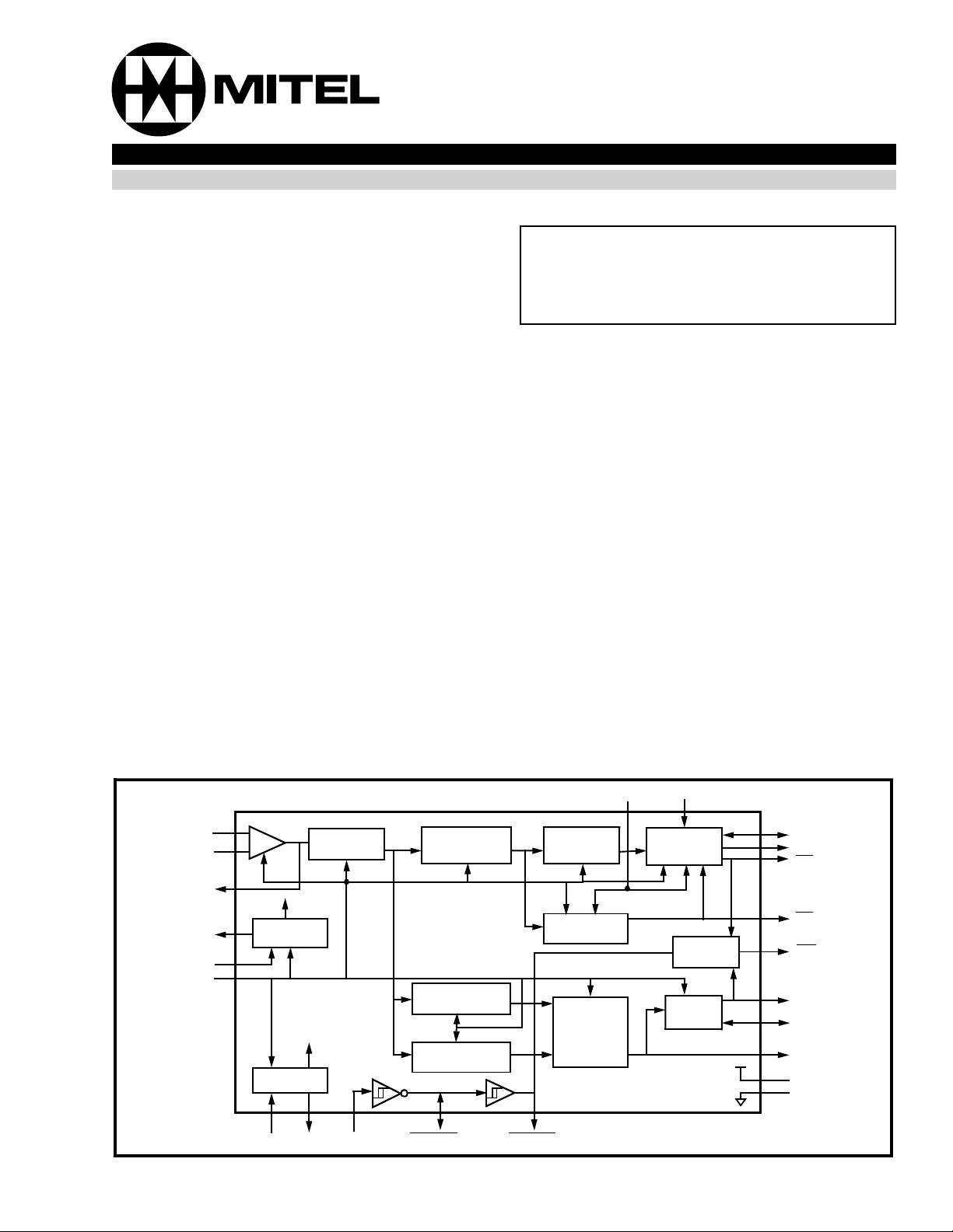
The MT8843 Calling Number Identification Circuit 2
(CNIC2) is a low power CMOS integrated circuit
intended for receiving physical layer signals
transmitted according to BT (British Telecom)
SIN227 & SIN242, CTA (Cable TV Association) TW/
P&E/312 and Bellcore TR-NWT-000030 & SR-TSV002476 specifications.
The CNIC2 provides all the features and functions
offered by Mitel’s MT8841 (CNIC), including 1200
baud BELL 202 and CCITT V.23 FSK demodulation.
The 3-wire serial FSK interface provided by CNIC
has been enhanced to operate in two modes. The
first mode is the CNIC compatible mode whereby
data transfer is initiated by the device. The new,
second mode allows a microcontroller to extract 8-bit
data words from the device. Furthermore, CNIC2
offers Idle State Tone Alert Signal and line reversal
detection capability for BT’s CLIP, ring burst
detection for CTA’s CLIP, and ring detection for
Bellcore’s CID.
IN+
IN-
GS
VRef
CAP
PWDN
+
-
Generator
Oscillator
OSCin OSCout
Anti-alias
To internal
cct.
Bias
To internal cct.
Filter
FSK Bandpass
Filter
Alert Signal High
Tone Filter
Alert Signal Low
Tone Filter
TRIGRCTRIGin
Demodulator
TRIGout
Figure 1 - Functional Block Diagram
FSK
Carrier
Detector
Tone
Detection
Algorithm
FSKen
MODE
Data Timing
Recovery
Interrupt
Generator
Guard
Time
DCLK
DATA
DR
CD
INT
StD
St/GT
ESt
VDD
VSS
5-21
Page 2

Preliminary Information MT8843
Pin Description
Pin # Na me Description
18 DR 3-wire FSK Interface Data Ready (CMOS Output). Active low.This output goes low after
the last DCLK pulse of eac h word. Th is ide ntifies the data (8 -bit word ) bound ary on the
serial output strea m. Typically, DR
converte r into a m icroc ontrol ler.
is used to latc h 8-bi t words from th e serial -to-p arallel
19 CD
Carrier Dete ct (C M OS O u tpu t). Active low. A logic low indicates the presence of in-band
signal a t the ou tput of t he FS K band pass filter.
20 INT
Interrupt (Open Drain Output). Active low. It is active when TRIGout or DR is low, or StD
is high. This output stays low until all three signals have become inactive.
21 StD Dual Tone Alert Signal Delayed Steering Output. When high, it indicates that a guard
time qua lifie d alert sig na l has bee n det ected .
22 ESt Dual Tone Alert Sign al Ea rly Ste ering Outp ut. Al ert signa l det ection ou tput. Use d in
conjuncti on wit h St/G T and ex terna l circui try to impleme nt de tect and non -det ect gua rd
times.
23 St/GT Dual Tone Alert Signal Steering Input/Guard Time (Analog Input/CMOS Output).
A voltage greater than V
pair and update the output latch. A voltage less than V
detected at St ca u s es t he device to re gi s t er the detected to ne
TGt
frees the d evi ce to acc ept a
TGt
new tone pa ir. The GT outpu t act s to re set th e ex ternal steerin g t im e-constant; its stat e is
a functio n of ESt and t he voltag e o n St.
24 V
Functional Overview
Positive Power Supply.
DD
alert signal as well as to receive and demodulate the
incoming CCITT V.23 FSK signals.
The MT8843 Calling Number Identification Circuit 2
(CNIC2) is a device compatible with BT, CTA and
Bellcore specifications. As shown in Figure 1, CNIC2
provides an FSK demodulator as well as a 3-wire
serial interface similar to that of it’s predecessor, the
MT8841 (CNIC). The 3-wire interface has been
enhanced to provide two modes of operation - a
mode whereby data transfer is initiated by the device
and a mode whereby data transfer is initiated by an
external microcontrolle r.
TW/P&E/312 proposes an alternate CDS TE
interface available for use in the CTA network.
According to TW/P&E/312, data is transmitted after a
single burst of ringing rather than before the first
ringing cycle (as specified in SIN227). The Idle State
Tone Alert Signal is not required as it is replaced with
a single ring burst. CNIC2 has the capability to
detect the ring burst. It is also able to demodulate
either Bell-202 or CCITT V.23 FSK data following the
ring burst, as specified by the CTA.
In addition to supporting all the features and
functions offered by MT8841, CNIC2 provides line
reversal detection, ring detection and dual tone alert
signal detection capability. These new functions
eliminate some external application circuitry
previously required with the MT8841 (CNIC).
SIN227 and SIN242 specify the signalling
mechanism between a network and a Terminal
Equipment (TE) providing Caller Display Service
(CDS). CDS provides Calling Line Identity
Presentation (CLIP), that is, delivery of the identity of
the caller when a telephone call arrives, before the
start of ringing (in the Idle State).
An incoming CDS call is indicated by a polarity
reversal on the A and B wires (line reversal),
followed by an Idle State Tone Alert Signal. CNIC2
has the capability to detect both the reversal and
TR-NWT-000030 specifies generic requirements for
transmitting asynchronous voiceband data to
Customer Premises Equipment (CPE). SR-TSV002476 describes the same requirements from the
CPE’s perspective. The data transmission technique
specified in both documents is applicable in a variety
of services like Calling Number Delivery (CND),
Calling Name Delivery (CNAM) and Calling Identity
Delivery on Call Waiting (CIDCW) - services
promoted by Bellcore.
In CND/CNAM service, information about a calling
party is embedded in the silent interval between the
first and second ring. CNIC2 detects the first ring and
can then be setup to receive and demodulate the
incoming Bell-202 FSK data. The device will output
the demodulated data onto a 3-wire serial interface.
5-23
Page 3

Preliminary Information MT8843
The diode bridge shown in Figure 3 half wave
rectifies a single ended ring signal. Full wave
rectification is achieved if the ringing is balanced. A
fraction of the ring voltage is applied to the TRIGin
input. When the voltage at TRIGin is above the
Schmitt trigger high going threshold VT+, TRIGRC is
pulled low as C3 discharges. TRIGout
stay s low as
long as the C3 voltage stays below the minimum
.
V
T+
In a CPE designed for CND/CNAM, TRIGout
high to
low transition may be used to interrupt or wake up
the microcontroller. The controller can thus be put
into sle ep mode to c onserve po w er.
Dual Tone Alert Signal Detect ion
According to SIN227 the Idle State Tone Alert Signal
allows more reliable detection of Caller Display
Service signals. The Idle State Tone Alert Signal
follows the line reversal and a silence period. The
characteristics of the BT’s idle state alerting tone is
shown in Table 1.
Item BT Bellcore
Low tone
2130Hz ±1.1% 2130Hz± 0.5%
frequency
High tone
2750Hz±1.1% 2750Hz±0.5%
frequency
Received
signal level
-2dBV to -40dBV
per tone on-hook
(0.22dBm
b
to
-14dBm to -32dBm
a
per tone off-hook
-37.78dBm)
Signal reject
level
Signal level
-46dBV
-45dBm
(-43.78dBm)
up to 7dB up to 6dB
differential
(twist)
c
Unwanted
signals
<= -20dB
(300-3400Hz)
Duration 88ms to 110ms
Speech
No Yes
<= -7dBm ASL
near end speech
d
75ms to 85ms
present
Table 1. Dual Tone Alert Signal Ch arac teri stics
a. The o ff-ho ok s ig na l le ve l is -15dB m to - 34 dB m pe r to ne to b e
specifie d in the BT CIDC W s pe c ifi ca ti on in th e future.
b. The si gn al po w er i s e xp res s ed in dBm r ef ere nc ed to 600 o hm
at the CPE A/B (tip/r ing) int erf ace.
c. ASL = ac ti ve s pe ec h le ve l ex pr e s sed in dBm referenc ed to
600 oh m at th e C P E ti p/ r in g i nte rf a c e. The l ev el is m easured
according to method B of Recommendation P.56 "Objective
Measurem e nt of Active Spee ch Lev el " publ is he d in th e CCI TT
Blue Book, volume V "Telephone Transmission Quality" 1989.
EPL (Equivalent Pe ak L evel ) = ASL+11.7dB
d. SIN2 27 s ug ge s ts tha t the recogn ition tim e sh ou ld be not le s s
than 20m s if both ton es a re detect ed .
Bellcore specifies a similar dual tone alert signal
called CPE Alerting Signal (CAS) for use in off-hook
data transmission. Bellcore states that the CPE
should be able to detect, in the presence of voice,
the CPE A lerti n g Sig nal.
The dual tone alert signal is separated into the high
and low tones with two bandpass filters. A detection
algorithm examines the two filter outputs to
determine the presence of a dual tone alert signal.
The ESt pin goes high when both tones are present.
Detect and non-detect guard times can be
implemented with external RC components. The
guard times improve detection performance by
rejecting signals of insufficient duration and masking
momentary detection dropout. StD is the guard time
qualified detector output.
• Dual Tone Detection Guard Time
When the dual tone alert signal is detected by the
CNIC2, ESt is pulled high. When the alerting signal
ceases to be detected, ESt goes low.
Figure 4 shows the relationship between the St/GT,
ESt and StD pins. It also shows the operation of a
guard time circuit. The guard time circuit improves
detection performance by rejecting detections of
insufficient duration and by allowing momentary ESt
dropouts once the duration criterion has been met.
The total recognition time is t
t
is the tone present guard time and tDP is the tone
GP
= tGP + tDP, where
REC
present detect time (refer to timing between ESt, St/
GT and StD in Figures 15 and 18).
The total tone absent time is t
t
is the tone absent guard time and tDA is the tone
GA
= tGA + tDA, where
ABS
absent detect time (refer to timing between ESt, St/
GT and StD in Figures 15 and 18).
Bellcore states that it is desirable for an off-hook
capable CPE to have a CAS detector on/off switch.
The switch was conceived so that a subscriber who
disconnects a service that relies on CAS detection
(e.g., CIDCW ), but retain s the CPE, can tu rn off the
detector and not be bothered by false detection.
SW1 in Figure 4 performs the above function. In the
B position, the comparator input, hence StD, is
always low. The CAS detector will not be enabled
and its output will not cause interrupts (except for the
system power up condition described in section
“Interrupt” on page 28’).
BT states that the idle state tone alert signal
recognition time should be no less than 20ms when
5-25
Page 4

Preliminary Information MT8843
Note that signals such as dual tone alert signal,
speech and DTMF tones lie in the same frequency
band as FSK. They will, therefore, be demodulated
and as a result, false data will be generated. To avoid
demodulation of false data, an FSKen pin is provided
so that the FSK demodulator may be disabled when
FSK signal is not expected.
The FSK characteristics described in Table 2 have
been specified i n BT and Bellcore specificat ions. The
BT signal frequencies correspond to CCITT V.23. The
Bellcore frequencies correspond to Bell 202. CTA
requires that the TE be able to receive both CCITT
V.23 and Bell 202, as specified in the BT and Bellcore
specifications. CN IC2 is compatible with both formats
with no external intervention.
Item BT Bellcore
Mark
frequency
1300Hz
± 1.5%
1200Hz
± 1%
(logic 1)
Space
frequency
2100Hz
± 1.5%
2200Hz
± 1%
(logic 0)
-32dBm
a
to
Received
signal level mark
-8dBV to
-40dBV
(-5.78dBm to
-12dBm
-37.78dBm)
Received
signal level -
-8dBV to
-40dBV
-12dBm to
-36dBm
space
Signal level
up to 6dB up to 10dB
b
differential
(twist)
Unwanted
signals
Transmission
rate
Word format 1 start bit (logic
<= -20dB
(300-3400Hz)
1200 baud
± 1%
0), 8 bit word
(LSB first), 1 to
10 stop bits
(logic 1)
<= -25dB
(200-3200Hz)
c
1200 baud
± 1%
1 start bit (logic
0), 8 bit word
(LSB first),
1 stop bit
(logic 1)
d
Table 2. FSK Characteristics
a. The s ig n al po w er is ex pressed in dB m re fe r en c ed to 60 0 o hm
at the CPE tip/ring (A/B) interface.
b. TR-N WT-000 03 0, Bulletin No. 1
c. The frequency range is specified in TR-NWT-000030.
d. Up to 20 m arks may b e in se rted in sp ec if ic pl ac e s i n a s in g le
or mult ip le da ta m es sag e.
• 3-wire User In terfa ce
The MT8843 provides a powerful dual mode 3-wire
interface so that the 8-bit data words in the
demodulated FSK bit stream can be extracted
without the need either for an external UART
(Universal Asynchronous Receiver Transmitter) or
for the TE/CPE’s microcontroller to perform the
UART function in software (asynchronous serial data
reception). The interface is specifically designed for
the 1200 baud rate and is comprised of the DATA,
DCLK (data clock) and DR
(data ready) pins. Two
modes (modes 0 and 1) are selectable via control of
the device’s MODE pin: in mode 0, data transfer is
initiated by the CNIC2; in mode 1, data transfer is
initiated by the external microcontroller.
Mode 0
This mode is selected when the MODE pin is low. It
is the CNIC (MT8841) compatible mode where data
transfer is initiated by the device.
In this mode, CNIC2 receives the FSK signal,
demodulates it, and outputs the extracted data to the
DATA pin (refer to Figure 12). For each receiv ed stop
and start bit sequence, the CNIC2 outputs a fixed
frequency clock string of 8 pulses at the DCLK pin.
Each clock rising edge occurs in the centre of each
DATA bit cell. DCLK is not generated for the stop and
start bits. Consequently, DCLK will clock only valid
data into a peripheral device such as a serial to
parallel shift register or a micro-controller. CNIC2
also outputs an end of word pulse (data ready) at the
pin. The data ready signal indicates the reception
DR
of every 10-bit word sent from the network to the TE/
CPE. This DR
signal is typically used to interrupt a
micro-controller.
Mode 1
This mode is selected when the MODE pin is high. In
this mode, the microcontroller supplies read pulses
(DCLK) to shift the 8-bit data words out of the
MT8843, onto the DATA pin. CNIC2 asserts DR
to
denote the word boundary and indicate to the
microprocessor that a new word has become
available (refer to Figure 14).
Internally, the MT8843’s demodulated data bits are
sampled and stored. After the 8th bit, the word is
parallel loaded into an 8 bit shift register and DR
goes low. The shift register’s contents are shifted out
to the DATA pin on DCLK’s rising edge in the order
they were re c eiv e d.
CNIC2 will meet these characteristics with its input
op-amp at unity gain.
If DCLK begins whil e DR
is low, DR will return to high
upon the first DCLK. This feature allows the
associated interrupt (see section on "Interrupt") to be
5-27
Page 5

Preliminary Information MT8843
The crystal specification is as follows:
Frequency:
Frequency tolerance:
Resonance mode
:Parallel
Load capacitance:
Maximum series resistance
Maximum drive level (mW):
3.579545 MHz
±0.1%(-40°C+85°C)
18 pF
: 150 ohms
2 mW
e.g., CTS MP036S
Any number of MT8843 devices can be connected
as shown in Figure 8 such that only one crystal is
required. The connection between OSC2 and OSC1
can be D.C. coupled as shown, or the OSC1 inputs
on all devices can be driven from a CMOS buffer (dc
coupled) with the OSC2 outputs left unconnected.
VRef and CAP Inputs
V
is the output of a low impedance voltage source
Ref
equal to V
A 0.1µF capacitor is required between CAP and V
to suppress noise on V
and is used to bias the input op-amp.
DD/2
Ref.
SS
Applications
The circuit shown in Figure 9 illustrates the use of the
MT8843 (CNIC2) device in a typica l CID or CLIP system. Network protection will differ depending on the
market for which the product is designed.
Notes:
CNIC2 has not been fully characterized for talkoff
and talkdown performance as specified in SR-TSV-
002476.
For CIDCW, speech immunity improves if near end
audio is cancelled from the incoming signal. One
possible implementation is to connect the signal
input to the 2 wire side when the CPE is on-hook and
the 4 wire side when the CPE is off-hook.
+5V
TIP / A
For BT network
protection:
TISP4180,
Notes
RING / B
Note: For CTA applications where there is a requirement to determine
the ring burst duration, the value of R and C may have to be optimized.
TISP5180,
TPA150A12 or
TPB150B12
0.1µF
0.1µF
0.01µF
0.01µF
500K
500K
430K
430K
200K
300K
34K
+5V
34K
+5V
C
500K
+5V
MT8843
CNIC2
IN+
464K
53K6
60K4
R
0.33µF
0.1µF
INGS
V
Ref
CAP
TRIGin
TRIGRC
TRIGout
MODE
OSCin
OSCout
V
SS
V
DD
St/GT
ESt
StD
INT
CD
DR
DATA
DCLK
FSKen
PWDN
= To microcontroller
= From microcontroller
(FSK Interface Mode 0 selecte d)
420K
420K
IC
0.1µF
0.1µF
+5V
100K
Figure 9 - Application Circuit
5-29
Page 6

Preliminary Information MT8843
DC Electrical Characteristics
Characteristics
TRIGout,
8
DCLK,
DA T A, DR
CD
, StD,
ESt , St/GT
TRIGRC
INT
9
IN+, IN-,
TRIGin
PWDN,
DCLK,
MODE,
FSKen
TRIGRC
10
11
12
13
14
† DC Electrical Characteristics are over recommended operating conditions unless otherwise stated.
Note 1 - Magnitude measurement, ignore signs.
INT
St/GT
V
Ref
St/GT
Output Low Sinking Current I
,
,
Input Current Iin1 1 µAVin=VDD or V
Output High-Impedance
Current
Output Voltage V
Comparator Threshold
Voltage
†
Sym
OL
Min Max Units Test Conditions
2.5 mA VOL=0.1*V
Iin2 10 µAVin=VDD or V
Ioz1 1 µAV
Ioz2 10 µA
Ioz3 5 µA
0.5V
Ref
V
TGt
0.5VDD-
0.05
0.05
DD
-
0.5VDD+
0.05
0.5VDD+
0.05
See Note 1
See Note 1
=VDD or V
out
See Note 1
V No Load
V
DD
SS
SS
SS
5-31
Page 7

Preliminary Information MT8843
Electrical Characteristics† - Gain Setting Amplifier
Characteristi cs Sym Min Typ
‡
Max Un its Test Conditions
1 Input Leakage Current I
2 Input Resistance R
3 Input Offset Voltage V
IN
OS
in
10 MΩ
1 µAVSS ≤ VIN ≤ V
25 mV
4 Power Supply Rejection Ratio PSRR 40 dB 1kHz ripple on V
5 Common Mode Rejection CMRR 40 dB V
6 DC Open Loop Voltage Gain A
7 Unity Gain Bandwidt h f
8 Output Voltage Swing V
9 Maximum Capacitive Load (GS) C
10 Maximum Resistive Load (GS) R
1 1 Common Mode Range Voltage V
† Electrical characteristics are over recommended operating conditions, unless otherwise stated.
‡ Typical figures are at 25°C and are for desi gn aid only: not guarantee d and not subje ct to producti on testing.
VOL
C
O
L
L
CM
0.5
50 kΩ
1.0
32 dB
0.3 MHz
VDD-0.5
V
pp
100 pF
VDD-1.0
V
≤ VIN ≤ V
CMmin
Load ≥ 50kΩ
AC Electrical Characteristics† - FSK Detection
Characteristi cs Sym Min Typ
1 Input Detection Level -40
-37.78
10.0
‡
Max Units Notes*
-8
-5.78
398.1
a
dBV
dBm
mVrms
1
b
DD
DD
CMmax
2 Transmission Rate 1188 1200 1212 baud
3 Input Frequency Detection
Bell 202 1 (Mark)
Bell 202 0 (Space)
CCITT V.23 1 (Mark)
CCITT V.23 0 (Space)
4 Input Noise Tolerance SNR
a. dBV = decibels above or below a reference voltage of 1Vrms.
b. dBm = decibels above or be low a reference power of 1mW into 60 0 ohms. 0dB m = 0.774 6Vrms.
*Notes
1. Both mark an d sp ac e have th e sa m e am pl itude.
2. Band limi ted random n oi s e ( 2 00 -3 400Hz). Pres ent whe n F SK si gn al is p r es en t. N ot e t ha t t he BT ba nd is 3 00 - 3 40 0H z , t he Bellcore
band i s 20 0- 3 20 0Hz .
† AC Electrical Characteristics are over recommended operating conditions, unless otherwise stated.
‡ Typical figures are at 25°C and are for desi gn aid only: not guarantee d and not subje ct to producti on testing.
FSK
1188
2178
1280.5
2068.5
1200
2200
1300
2100
1212
2222
1319.5
2131.5
Hz
Hz
Hz
Hz
20 dB 1,2
5-33
Page 8

Preliminary Information MT8843
DATA
DCLK
Figure 10 - DATA and DCLK Mode 0 Output Timing*
*VHM=0.7*VDD, VLM=0.3*VDD, VCT=0.5*V
DR
t
DCD
t
R
t
CL
DD
t
RF
t
DH, tDL
t
R
t
RL
t
CDD
t
RR
t
CH
t
F
V
HM
V
CT
V
LM
V
HM
V
CT
V
LM
t
F
V
HM
V
CT
V
LM
*VHM=0.7*VDD, VLM=0.3*VDD, VCT=0.5*V
start
stop
A/B WIRES
t
IDD
b7
10
b0 b1 b2 b3 b4 b5
start
DATA
b7 b0 b1 b2 b3 b4 b5
stop
DCLK
DR
Figure 12 - Serial Data Interface Timing (MODE 0)
DD
Figure 11 - DR Out put Timi ng*
start
stop
b6
b7
b6
b7 b0 b1 b2 b3 b4 b5
1/f
t
CRD
b0 b1 b2 b3 b4 b5
10
start
stop
DCLK0
t
RL
b6
b7
b6
start
stop
10
b7
b0 b1 b2
start
b0 b1 b2
stop
5-35
Page 9
Preliminary Information MT8843
Alerting Signal
Line Reversal
A/B Wires
TRIGout
PWDN
ESt
St/GT
StD
TE DC load
TE AC load
FSKen
CD
DR
DCLK
DATA
OSCout
Ch. seizure
Mark
Data Packet
AB C D E F G
t
DA
Note 6
t
GA
V
TGt
t
(Note 1)
ABS
15±1ms
< 0.5mA (optional)
Current wetting pulse (see SIN227)
Zss (Refer to SIN227)
t
CP
..101010.. Data
Note 5
t
DP
t
t
GP
REC
<120µA
20±5ms
Ring
Note 4
50-150ms
Note 2
Note 3
t
CA
A ≥ 100ms
B = 88-110ms
C ≥ 45ms (up to 5sec)
D = 80-26 2 ms
E = 45-75 ms
F ≤ 2.5sec (ty p. 500 ms)
G > 20 0m s
Note: All values obtained
from SIN227 Issue 1
Notes:
Figure 15 - Input and Output Timing for BT Caller Display Service (CDS), e.g., CLIP
1) By ch oo si ng t
edge.
2) SIN2 27 sp ecifies that th e AC a nd D C loa ds sh ou ld be re mov ed be tw e en 50-150ms afte r the en d of the FS K s ig na l, in d ic ate d b y C D
returnin g to high. Th e C NI C2 m ay a ls o be po w er ed down at th is ti me .
3) FSKen sh ou ld be se t lo w w he n F SK is not expe cte d to p rev en t th e FSK dem od u lat or from reac tin g to other in - ba nd s ign a ls su ch as
speech, to ne al er t s ign a l a nd D TM F tones.
4) TRIGo ut
5) The to ta l re c og ni tion time i s t
to sectio n “Dual Tone Detect io n G u ard Time” on page 25 fo r d etails).
6) The to ta l t on e a bs e nt t im e is t
to sectio n “Dual Tone Detect io n G u ard Time” on page 25 fo r d etails).
V
is the c om pa rat or thre s ho ld ( re fer to Figure 4 ).
TGt
=15ms, t
GA
will be 15 - 25 m s so tha t the curren t we tti ng pulse a nd AC l oa d c an b e a pp lie d right afte r th e StD falli ng
ABS
is the r in g en ve lo pe d ur i ng rin gi ng .
= tGP + tDP, where tGP is the to ne presen t g ua r d t im e an d tDP is the to ne present d et ec t ti m e (refer
REC
= tGA + tDA, where tGA is the tone abse nt gu ar d ti me and tDA is the to ne ab s ent d ete c t ti me (re fe r
ABS
5-37
Page 10

Preliminary Information MT8843
TIP/RING
TRIGout
PWDN
OSCout
FSKen
CD
1st Ring 2nd RingCh. seizure
ACDEF
Note 1
Note 2
B
t
CP
Mark Data Packet
t
CA
Note 3
Note 1
Note 4
A = 2sec typical
B = 250-500ms
DR
C = 250ms
D = 150ms
DCLK
E = feature specific
Max C+D+E = 2.9 to 3.7sec
F ≥ 200ms
DATA
..101010..
Data
Figur e 1 7 - I npu t and O utp u t Ti m i n g for Bellc ore On-ho ok Data Transmissio n Associated with
Ringing, e.g., CID
Notes:
This on- h oo k ca se a pp li ca t io n is in c lud e d b ec ause a CIDCW ( off-h oo k) CP E s h ou ld also b e c a pa bl e o f re c ei vi ng on-hook da ta
transmission (with ringing) from the end office. TR-NWT-000575 specifies that CIDCW will be offered only to lines which subscribe to
CID.
1) The CPE designer may choose to enable the CNIC2 only after the end of ringing to conserve power in a battery operated CPE. CD
activated by ringing.
2) The CP E d es ig ner m ay c h oose to set FS K en al w ay s high whil e the CPE is o n-h oo k. Setting FSKen low p r events the FS K
demodul ato r f rom r e ac ti ng to ot her in-b an d si gn al s such as speech, CA S o r D T MF tones.
3) The mic r o co nt rol ler in the C PE po wer s d own th e CNIC2 af ter C D
4) The m ic ro co nt r ol le r ti me s ou t i f C D
is not ac tiv a ted.
has bec om e in ac ti ve .
is not
5-39
 Loading...