

Page 1

E2O0016-39-81
¡ Semiconductor MSM82C37B-5RS/GS/VJS
¡ Semiconductor
This version: Aug. 1999
Previous version: Jan. 1998
MSM82C37B-5RS/GS/VJS
PROGRAMMABLE DMA CONTROLLER
GENERAL DESCRIPTION
The MSM82C37B-5RS/GS/VJS, DMA (Direct Memory Access) controller is capable of highspeed data transfer without CPU intervention and is used as a peripheral device in microcomputer
systems. The device features four independent programmable DMA channels.
Due to the use of silicon gate CMOS technology, standby current is 10 mA (max.), and power
consumption is as low as 10 mA (max.) when a 5 MHz clock is generated.
All items of AC characteristics are compatible with intel 8237A-5.
FEATURES
• Maximum operating frequency of 5 MHz (Vcc = 5 V ±10%)
• High-speed operation at very low power consumption due to silicon gate CMOS technology
• Wide operating temperature range from –40°C to +85°C
• 4-channels independent DMA control
• DMA request masking and programming
• DMA request priority function
• DREQ and DACK input/output logic inversion
• DMA address increment/decrement selection
• Memory-to-Memory Transfers
• Channel extension by cascade connection
• DMA transfer termination by EOP input
• Intel 8237A-5 compatibility
• TTL Compatible
• 40-pin Plastic DIP (DIP40-P-600-2.54): (Product name: MSM82C37B-5RS)
• 44-pin Plastic QFJ (QFJ44-P-S650-1.27): (Product name: MSM82C37B-5VJS)
• 44-pin Plastic QFP (QFP44-P-910-0.80-2K): (Product name: MSM82C37B-5GS-2K)
1/33
Page 2
¡ Semiconductor MSM82C37B-5RS/GS/VJS
PIN CONFIGURATION (TOP VIEW)
40 pin Plastic DIP
44 pin Plastic QFP
6A7
38
A5A4EOP
A
37
36
NC
MEMW
MEMR
IOW
IOR
NC
44
43
42
41
40
39
READY
ADSTB
RESET
DACK
DACK
1
HLDA
2
3
AEN
4
HRQ
5
NC
6
7
CS
8
CLK
9
10
2
11 DB
3
35
34
33
32
31
30
29
28
27
26
25
24
23
A
A
A
A
V
NC
DB
DB
DB
DB
1
IOR
2
IOW
3
MEMR
MEMW
READY
ADSTB
3
2
1
0
CC
0
1
2
3
4
4
5
NC
6
7
HLDA
8
9
AEN
10
HRQ
11
CS
12
CLK
13
RESET
DACK
14
2
DACK
15
3
DREQ
16
3
DREQ
17
2
DREQ
18
1
DREQ
19
0
20
GND
44 pin Plastic QFJ
40
39
38
37
36
35
34
33
32
31
30
29
28
27
26
25
24
23
22
21
A
7
A
6
A
5
A
4
EOP
A
3
A
2
A
1
A
0
V
CC
DB
0
DB
1
DB
2
DB
3
DB
4
DACK
DACK
DB
5
DB
6
DB
7
(+5 V)
0
1
12
13
3
DREQ
DREQ2DREQ1DREQ
14
15
16
17
18
19
20
21
0
GND
NC
DB
7
6DB5
DB
22
0
DACK1DACK
READY
HLDA
ADSTB
RESET
DACK2
NC
AEN
HRQ
CS
CLK
NC
10
11
12
13
14
15
16
17
7
NC
6
MEMW
MEMR
5
4
IOW
3
IORNCA
2
6A5A4
A
1
43
44
7
8
9
18
19
20
21
22
23
24
25
7
3
DACK
DREQ3DREQ2DREQ1DREQ
0
GND
DB
6DB5
DB
42
26
EOP
41
40
27
28
0
DACK1DACK
39
38
37
36
35
34
33
32
31
30
29
V
NC
A
A
A
A
DB
DB
DB
DB
DB
3
2
1
0
CC
0
1
2
3
4
2/33
Page 3
¡ Semiconductor MSM82C37B-5RS/GS/VJS
BLOCK DIAGRAM
IOR
MEMR
MEMW
READY
ADSTB
RESET
DREQ
DACK
IOW
AEN
CS
CLK
EOP
HLDA
HRQ
0 - 3
0 - 3
4
Judgment
4
Timing
Control
Circuit
Priority
Circuit
TC
(Terminal Count)
Mode
Register
¥
16)
(4
Command
Register (8)
Mark
Register (4)
Request
Register (4)
Decrementer
Temporary Word
Count Register (16)
Base Word
Count
Register
(4 ¥ 16)
16 Bit Bus
Current
Word
Count
Register
(4 ¥ 16)
Status
Register (8)
Incrementer/Decrementer
Temporary Address
Register (16)
16 Bit Bus
Base
Address
Register
(4 ¥ 16)
Internal Data Bus
Temporary
Register (8)
Current
Address
Register
(4 ¥ 16)
8 4
15
- A
8
A
Output
Buffer
4
Input/Output
Buffer
Command
Control
Circuit
2
D
0 - 1
Input/Output
Buffer
A
DB
4 - A7
A
0 - A3
0 - DB7
3/33
Page 4
¡ Semiconductor MSM82C37B-5RS/GS/VJS
ABSOLUTE MAXIMUM RATINGS
Parameter Unit
Power Supply Voltage
Input Voltage
Output Voltage
Storage Temperature
Power Dissipation
Symbol
V
CC
V
IN
V
OUT
T
STG
P
D
Conditions
with respect
to GND
—
Ta = 25°C
MSM82C37B-5RS
1.0
MSM82C37B-5GS
–0.5 to +7
–0.5 to V
–0.5 to V
CC
CC
+0.5
+0.5
–55 to +150
0.7
MSM82C37B-5VJS
RECOMMENDED OPERATING CONDITIONS
Rating
Parameter UnitSymbol
Power Supply Voltage
Operating Temperature
"L" Input Voltage
"H" Input Voltage
Min.
V
CC
T
op
V
IL
T
IH
4.5
–40
–0.5
2.2
Typ.
5.0
+25
—
—
V
CC
Max.
5.5
+85
+0.8
+ 0.5
DC CHARACTERISTICS
1.0
V
V
V
°C
W
V
°C
V
V
Parameter Symbol
"L" Output Voltage V
"H" Output Voltage
Input Leak Current I
Output Leak Current I
Average Power Supply
Current during Operations
Power Supply Current
in Standby Mode
V
I
I
CCS
LO
CC
OL
OH
LI
Conditions
I
= 3.2 mA
OL
I
= –1.0 mA
OH
IN
OUT
£ V
£ V
CC
CC
0V £ V
0V £ V
Input frequency
5 MHz, when RESET
V
= 0 V/VCC,
IN
C
= 0 pF
L
= 0 V,
HLDA
V
= 0 V,
IL
V
= V
CC
IH
V
= 4.5 V
CC
to 5.5 V
Ta
= –40°C
to +85°C
Min.
—
3.7
–10
–10
—
—
Typ.
—
—
—
—
—
—
Max.
0.4
—
10
10
10
10
Unit
V
V
mA
mA
mA
mA
4/33
Page 5
¡ Semiconductor MSM82C37B-5RS/GS/VJS
AC CHARACTERISTICS
DMA (Master) Mode
(Ta = –40 to +85°C, VCC = 4.5 to 5.5 V)
Symbol
Item
Min. Max. Unit
Comments
t
AEL
t
AET
t
AFAB
t
AFC
t
AFDB
t
AHR
t
AHS
t
AHW
Delay Time from CLK Falling Edge
up to AEN Leading Edge
Delay Time from CLK Rising Edge
up to AEN Trailing Edge
Delay Time from CLK Rising Edge
up to Address Floating Status
Delay Time from CLK Rising Edge
up to Read/Write Signal Floating Status
Delay Time from CLK Rising Edge
up to Data Bus Floating Status
Address Valid Hold Time
to Read Signal Trailing Edge
Data Valid Hold Time
to ADSTB Trailing Edge
Address Valid Hold Time
to Write Signal Trailing Edge
Delay Time from CLK Falling Edge
up to Active DACK
——200
——130
——90
——120
——170
tCY – 100 ——
30 ——
tCY – 50 ——
— (Note 3)170
ns
ns
ns
ns
ns
ns
ns
ns
ns
t
t
ASM
t
ASS
t
t
t
AK
CH
CL
CY
Delay Time from CLK Rising Edge
up to EOP Leading Edge
Delay Time from CLK Rising Edge
up to EOP Trailing Edge
Time from CLK Rising Edge
up to Address Valid
Data Set-up Time to ADSTB Trailing Edge
Clock High-level Time
Clock Low-level Time
CLK Cycle Time
— (Note 5)170
——170
——170
100 ——
68 (Note 6)—
68 (Note 6)—
200 ——
ns
ns
ns
ns
ns
ns
ns
5/33
Page 6

¡ Semiconductor MSM82C37B-5RS/GS/VJS
DMA (Master) Mode (continued)
Symbol
t
DCL
t
DCTR
t
DCTW
t
DQ
t
EPS
t
EPW
t
FAAB
t
FAC
t
FADB
Item
Delay Time from CLK Rising Edge
to Read/Write Signal Leading Edge
Delay Time from CLK Rising Edge
to Read Signal Trailing Edge
Delay Time from CLK Rising Edge
to Write Signal Trailing Edge
Delay Time from CLK Rising Edge
to HRQ Valid
EOP Leading Edge Set-up Time to
CLK Falling Edge
EOP Pulse Width
Delay Time from CLK Rising Edge
to Address Valid
Time from CLK Rising Edge
up to Active Read/Write Signal
Delay Time from CLK Rising Edge
to Data Valid
Min. Max. Unit
— (Note 2)190
— (Note 2)190
— (Note 2)130
——120
40 ——
220
——170
——150
——200
ns
ns
ns
ns
ns
ns
ns
ns
ns
Comments
——
t
t
t
t
ODH
t
ODV
t
t
t
t
HS
IDH
IDS
QS
RH
RS
STL
HLDA Valid Set-up Time
to CLK Rising Edge
Input Data Hold Time
to MEMR Trailing Edge
Input Data Set-up
to MEMR Trailing Edge
Output Data Hold Time
to MEMW Trailing Edge
Time from Output Data Valid
to MEMW Trailing Edge
DREQ Set-up Time
to CLK Falling Edge
READY Hold Time
to CLK Falling Edge
READY Set-up Time
to CLK Falling Edge
Delay Time from CLK Rising Edge
to ADSTB Leading Edge
75 ——
0——
170 ——
10 ——
125 ——
0 (Note 3)—
20 ——
60 ——
——130
ns
ns
ns
ns
ns
ns
ns
ns
ns
t
STT
Delay Time from CLK Rising Edge
to ADSTB Trailing Edge
——90
ns
6/33
Page 7

¡ Semiconductor MSM82C37B-5RS/GS/VJS
Slave Mode
Symbol
t
t
AW
t
CW
t
DW
t
t
RDE
t
RDF
t
RSTD
AR
RA
Time from Address Valid or
CS Leading Edge to IOR Leading Edge
Address Valid Set-up Time
to IOW Trailing Edge
CS Leading Edge Set-up Time
to IOW trailing edge
Data Valid Set-up Time
to IOW Trailing Edge
Address or CS Hold Time
to IOR Trailing Edge
Data Access Time
to IOR Leading Edge
Delay Time to Data Floating Status
from IOR Trailing Edge
Supply Power Leading Edge Set-up
time to RESET Trailing Edge
Item
(Ta = –40 to +85°C, VCC = 4.5 to 5.5 V)
Min. Max. Unit
50 ——
130 ——
130 ——
130 ——
0——
——140
0—70
500 ——
ns
ns
ns
ns
ns
ns
ns
ns
Comments
t
RSTS
t
RSTW
t
RW
t
WA
t
WC
t
WD
t
WWS
Time to First Active IOR or IOW
from RESET Trailing Edge
RESET Pulse Width
IOR Pulse Width
Address Hold Time
to IOW Trailing Edge
CS Trailing Edge Hold Time
to IOW Trailing Edge
Data Hold Time to IOW Trailing Edge
IOW Pulse Width
Notes: 1. Output load capacitance of 150 (pF).
2. IOW and MEMW pulse widths of tCY – 100 (ns) for normal writing, and 2tCY – 100
(ns) for extended writing. IOR and MEMR pulse widths of 2tCY – 50 (ns) for normal
timing, and tCY – 50 (ns) for compressed timing.
3. DREQ and DACK signal active level can be set to either low or high. In the timing
chart, the DREQ signal has been set to active-high, and the DACK signal to activelow.
4. When the CPU executes continuous read or write in programming mode, the
interval during which the read or write pulse becomes active must be set to at least
400 ns.
5. EOP is an open drain output. The value given is obtained when a 2.2 kW pull-up
resistance is connected to VCC.
6. Rise time and fall time are less than 10 ns.
7. Waveform measurement points for both input and output signals are 2.2 V for HIGH
and 0.8 V for LOW, unless otherwise noted.
2t
CY
300 ——
200 ——
20 ——
20 ——
30 ——
160 ——
ns
ns
ns
ns
ns
ns
ns
——
7/33
Page 8
¡ Semiconductor MSM82C37B-5RS/GS/VJS
TIMING CHART
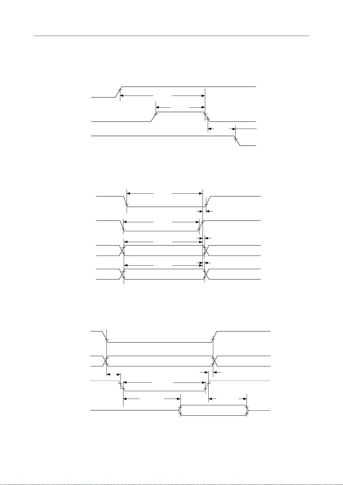
Reset Timing
V
CC
RESET
IOR, IOW
Slave Mode Write Timing
CS
t
RSTD
t
CW
t
RSTW
t
RSTS
t
WC
IOW
A
- A
0
3
DB0 - DB
7
Slave Mode Read Timing
CS
- A
A
0
3
IOR
t
WWS
t
t
AW
WA
Input Valid Address
t
t
DW
WD
Input Valid Data
Input Valid Address
t
AR
t
RW
t
RA
DB
- DB
0
t
RDE
7
Output Valid Data
t
RDF
8/33
Page 9
¡ Semiconductor MSM82C37B-5RS/GS/VJS
(Input)
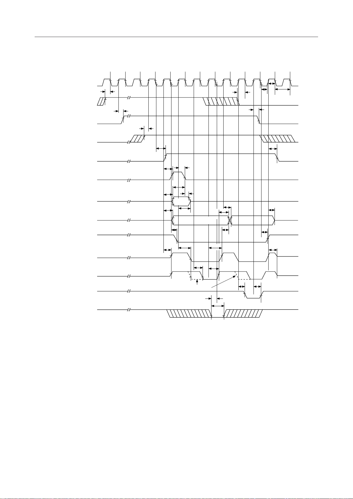
DMA Transfer Timing
CLK
DREQ
HRQ
HLDA
AEN
ADSTB
- DB
DB
0
A0 - A
DACK
IOR, MEMR
SI SI S0S0S1S
t
QS
t
DQ
t
HS
t
7
7
AEL
t
t
t
STL
FADB
FAAB
S3S
2
t
STT
t
ASS
t
AHS
A8 - A
15
t
AFDB
A0 - A
t
AK
t
FAC
DCL
t
DCL
t
S2S3S
4
t
ASM
t
AHW
7
t
DCTR
t
DCTW
t
AHR
t
QS
t
DQ
A0 - A
4
t
AK
t
CL
7
SI SI
t
CH
t
CY
t
AET
t
AFAB
t
AFC
IOW, MEMW
Internal EOP
(Output)
External EOP
(Extended Write)
t
EPS
t
EPW
t
t
AK
AK
9/33
Page 10
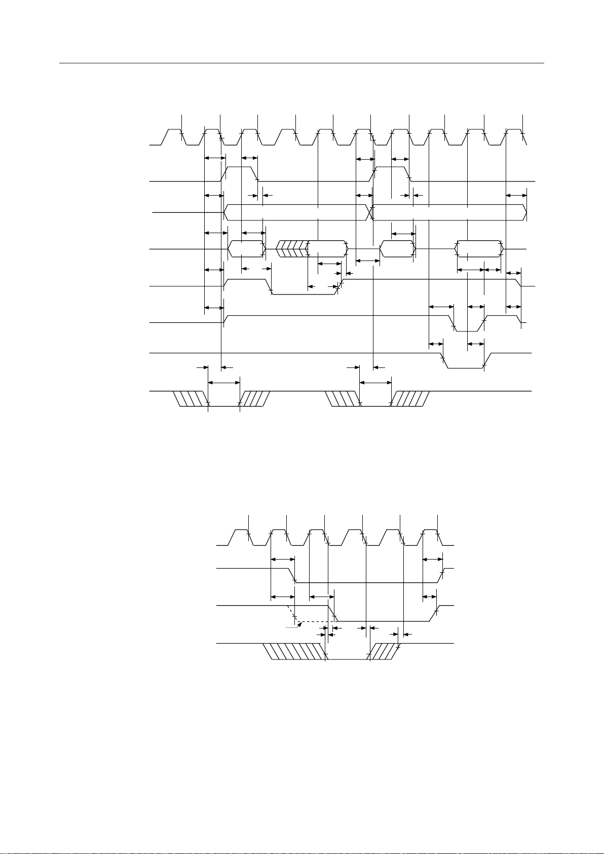
¡ Semiconductor MSM82C37B-5RS/GS/VJS
(Input)
Memory to Memory Transfer Timing
CLK
ADSTB
A0 - A
DB
- DB
0
MEMR
MEMW
Internal EOP
(Output)
External EOP
S
S
0
t
FAAB
7
t
FADB
7
t
EPS
11
S
12
t
STL
t
A8 - A
t
FAC
t
FAC
t
EPW
S
13
STT
t
AHS
Valid Address A
t
AFDB
15
t
DCL
S
14
0 - 7
Data Input
t
DCTR
t
IDS
S
t
EPS
S
21
t
t
t
IDH
STL
ASM
t
FADB
t
22
A8 - A
EPW
S
23
t
STT
t
AHS
Valid Address A
t
AFDB
15
S
24
SI
t
AFAB
0 - 7
Data Output
t
ODVtODH
t
t
DCL
t
AK
DCTW
t
AK
t
AFC
t
AFC
Ready Timing
CLK
IOR, MEMR
IOW, MEMW
READY
S
2
(Extended Write)
S
t
DCL
t
DCL
t
RS
S
3
W
t
DCL
t
RH
S
t
S
W
RH
4
t
DCTR
t
DCTW
t
RS
10/33
Page 11
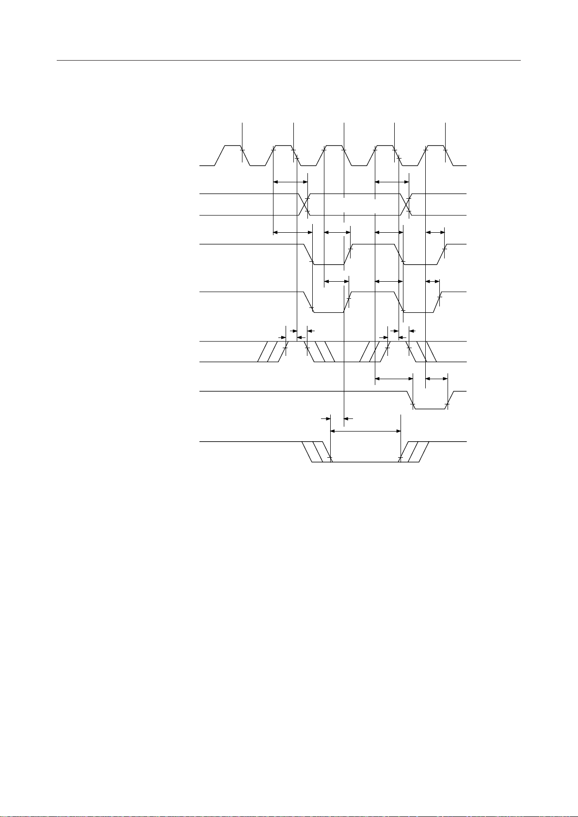
¡ Semiconductor MSM82C37B-5RS/GS/VJS
(Input)
Compressed Transfer Timing
CLK
A
- A
0
IOR, MEMR
IOW, MEMW
READY
Internal EOP
(Output)
S
2
t
ASM
7
t
t
RS
DCL
S
4
t
RH
t
EPS
Valid Address
t
DCTR
t
DCTW
t
S
EPW
2
t
ASM
t
DCL
t
DCL
t
RS
S
4
t
DCTR
t
DCTW
t
RH
t
AK
t
AK
External EOP
11/33
Page 12

¡ Semiconductor MSM82C37B-5RS/GS/VJS
PIN FUNCTIONS
Symbol
V
CC
GND —
CLK Input
CS Input
RESET Input
READY Input
HLDA Input
-
DREQ
0
DREQ
3
Pin Name
Power
Ground
Clock
Chip Select
Reset
Ready
Hold Acknowledge
DMA Request
0 - 3 Channels
Input/Output
—
Input
Function
+5 V power supply
Ground (0 V) connection.
Control of MSM82C37B-5 internal operations and data transfer
speed.
CS is active-low input signal used for the CPU to select
the MSM82C37B-5 as an I/O device in an idle cycle.
RESET is active-high asynchrounous input signal used to clear
command, status, request, temporary registers, and first/last F/F,
and to set mask register. The MSM82C37B-5 enters an idle cycle
following a RESET.
The read or write pulse width can be extended to accomodate
slow access memories and I/O devices when this input is
switched to low level. Note this input must not change within
the prescribed set-up/hold time.
HLDA is active-high input signal used to indicate that system bus
control has been released when a hold request is recieved by
the CPU.
DREQ is asynchronous DMA transfer request input signals.
Although these pins are switched to active-high by reset, they can
be programmed to become active-low. DMA requests are
received in accordance with a prescribed order of priority. DREQ
must be held until DACK becomes active.
DB
- DB
0
IOR Input/Output
IOW Input/Output
Data Bus 0 - 7
7
I/O Read
I/O Write
Input/Output
DB is bidirectional three-state signals connected to the system
data bus, and which is used as an input/output of MSM82C37B-5
internal registers during idle cycles, and as an output of the eight
higher order bits of transfer addresses during active cycles.
Also used as input and output of transfer data during memorymemory transfers.
IOR is active-low bidirectional three-state signal used as an input
control signal for CPU reading of MSM82C37B-5 internal
registers during idle cycles, and as an output control signal for
reading I/O device transfer data in writing transfers during active
cycles.
IOW is active-low bidirectional three-state signal used as an input
control signal for CPU writing of MSM82C37B-5 internal registers
during idle cycles, and as an output control signal for writing I/O
device transfer data in writing transfers during active cycles.
12/33
Page 13

¡ Semiconductor MSM82C37B-5RS/GS/VJS
PIN FUNCTIONS (continued)
Symbol
EOP Input/Output
- A
A
0
3
A
- A
4
7
HRQ Output
Pin Name
End of Process
Address 0 - 3
Address 4 - 7
Hold Request
Input/Output
Input/Output
Output
Function
EOP is active-low bidirectional three-state signal. Unlike other
pins, this pin is an N-channel open drain. During DMA operations,
a low-level output pulse is obtained from this pin if the channel
word count changes from 0000H to FFFFH.
And DMA transfers can be terminated by pulling the EOP input to
low level. Both of these actions are called terminal count (TC).
When internal or external EOP is generated, the MSM82C37B-5
terminates the transfer and resets the DMA request.
When the EOP pin is not used, it is necessary to hold the pin at
high level by pull-up resistor to prevent the input of an EOP
by error. Also note that the EOP function cannot be satisfied in
cascade mode.
A
- A3 is bidirectional three-state signals used as input signals
0
for specifying the MSM82C37B-5 internal register to be accessed
by the CPU during idle cycles, and as an output the four lower
order bits of the transfer address during active cycles.
A
- A7 is three-state signals used as an output the four higher
4
order bits of the transfer address during active cycles.
HRQ is active-high signal used as an output of hold request to
the CPU for system data bus control purposes. After HRQ has
become active, at least one clock cycle is required before HLDA
becomes active.
DMA Acknowledge
-
DACK
0
DACK
AEN Output
ADSTB Output
MEMR Output
MEMW Output
0 - 3 Channels
3
Address Enable
Address Strobe
Memory Read
Memory Write
Output
DACK is output signals used to indicate that DMA transfer to
peripheral devices has been permitted. (Available in each channel.)
Although these pins are switched to active-low when reset, they
can be programmed to become active-high.
Note that there is no DACK output signal during memory-memory
transfers.
AEN is active-high ouput signal used to indicate that output
signals sent from the MSM82C37B-5 to the system are valid.
And in addition to enabling external latch to hold the eight higher
order bits of the transfer address, this signal is also used to
disable other system bus buffers.
ADSTB is active-high signal used to strobe the eight higher order
bits of the transfer address by external latch.
MEMR is active-low three-state output signal used as a control
signal in reading data from memory during read transfers and
memory-memory transfers.
MEMW is active-low three-state output signal used as a control
signal in writing data into memory during write transfers and
memory-memory transfers.
13/33
Page 14

¡ Semiconductor MSM82C37B-5RS/GS/VJS
RESET
SI
N
N
EOP F/F Setting
External DMA
Request
external DMA
Memory-Memory
Y
External EOP
Compressed
Y
Y
External EOP
Y
Single Transfer
N
Y
Demand Transfer
Y
Carry or Borrow
Internal/
Request
Y
S
0
HLDA
Y
Transfer
N
S
1
S
2
N
Timing
N
S
3
Verify
N
READY
Y
S
4
Internal/
N
N
HLDA
Y
N
Y
N
Y
S
11
S
12
External EOP
N
S
13
Y
READY
Y
EOP F/F Setting
N
SW
Y
S
14
S
21
S
N
SW
22
External EOP
N
S
23
READY
Y
EOP F/F Setting
N
SW
Y
S
24
Internal/
External EOP
Y
N
Y
N
HLDA
N
Note:
Y º Yes (Active)
N º No (Inactive)
Figure 1 DMA Operation State Transition Diagram
14/33
Page 15

¡ Semiconductor MSM82C37B-5RS/GS/VJS
OUTLINE OF FUNCTIONS
The MSM82C37B-5 consists of five blocks = three logic sections, an internal register section, and
a counter section.
The logic sections include a timing control block where the internal timing and external control
signals are generated, a command control block where each instruction from the CPU is
decoded, and a priority decision block where the order of DMA channel priority is determined.
The purpose of the internal register section is to hold internal states and instructions from the
CPU, while the counter section computes addresses and word counts.
DESCRIPTION OF OPERATIONS
The MSM82C37B-5 operates in two cycles (called the idle and active cycles) which are divided
into independent states. Each state is commenced by a clock falling edge and continues for a
single clock cycle. The transition from one state to the next in DMA operations is outlined in
Figure 1.
Idle Cycle
The idle cycle is entered from the Sl state when there is no valid DMA request on any
MSM82C37B-5 channel. During this cycle, DREQ and CS inputs are monitored during each
cycle. When a valid DMA request is then received, an active cycle is commenced. And if the
HLDA and CS inputs are at low level, a programming state is started with MSM82C37B-5
reading or writing executed by IOR or IOW. Programming details are described later.
Active Cycle
If a DMA request is received in an unmasked channel while the MSM82C37B-5 is in idle cycle,
or if a software DREQ is generated, the HRQ is changed to high level to commence an active
cycle. The initial state of an active cycle is the S0 state which is repeated until the HLDA input
from the CPU is changed to high level. (But because of internal operational reasons, a minimum
of one clock cycle is required for the HLDA is be changed to high level by the CPU after the HRQ
has become high level. That is, the S0 state must be repeated at least twice.)
After the HLDA has been changed to high level, the S0 state proceeds to operational states S1
thru S4 during I/O-memory transfers, or to operational states S11 thru S14 and S21 thru S
24
during memory-memory transfers.
If the memory or I/O device cannot be accessed within the normal timing, an SW state (wait
state) can be inserted by a READY input to extend the timing.
15/33
Page 16

¡ Semiconductor MSM82C37B-5RS/GS/VJS
DESCRIPTION OF TRANSFER TYPES
MSM82C37B-5 transfers between an I/O and memory devices, or transfers between memory
devices. The three types of transfers between I/O and memory devices are read, write, and
verify.
I/O-Memory Transfers
The operational states during an I/O-memory transfer are S1, S2, S3, and S4.
In the S1 state, an AEN output is changed to high level to indicate that the control signal from
the MSM82C37B-5 is valid. The eight lower order bits of the transfer address are obtained from
A0 thru A7, and the eight higher order bits are obtained from DB0 thru DB7. The ADSTB output
is changed to high level at this time to set the eight higher order bits in an external address latch,
and the DACK output is made active for the channel where the DMA request is acknowledged.
Where there is no change in the eight higher bit transfer address during demand and block mode
transfers, however, the S1 state is omitted.
In the S2 state, the IOR or MEMR output is changed to low level.
In the S3 state, IOW or MEMW is changed to low level. Where compressed timing is used,
however, the S3 state is omitted.
The S2 and S3 states are I/O or memory input/output timing control states. In the S4 state, IOR,
IOW, MEMR, and MEMW are changed to high level, and the word count register is decremented
by 1 while the address register is incremented (or decremented) by 1. This completes the DMA
transfer of one word.
Note that in I/O-memory transfers, data is transferred directly without being taken in by the
MSM82C37B-5. The differences in the three types of I/O-memory transfers are indicated below.
Read Transfer
Data is transferd from memory to the I/O device by changing MEMR and lOW to low level.
MEMW and IOR are kept at high level during this time.
Write Transfer
Data is transferred from the I/O device to memory by changing MEMW and IOR to low level.
MEMR and IOW are kept at high level during this time.
Note that writing and reading in these write and read transfers are with respect to the memory.
Verify Transfer
Although verify transfers involve the same operations as write and read transfers (such as
transfer address generation and EOP input responses),they are in fact pseudo transfers where
all I/O and memory reading/writing control signals are kept inactive. READY inputs are
disregarded in verify transfers.
16/33
Page 17

¡ Semiconductor MSM82C37B-5RS/GS/VJS
Memory-memory Transfer
Memory-memory transfers are used to transfer data blocks from one memory area to another.
Memory-memory transfers require a total of eight states to complete a single transfer four states
(S11 thru S14) for reading from memory, and four states (S21 thru S24) for writing into memory.
These states are similar to I/O-memory transfer states, and are distinguished by using two-digit
numbers. In memory-memory transfers, channel 0 is used for reading data from the source area,
and channel 1 is used for writing data into the destination area. During the initial four states,
data specified by the channel 0 address is read from the memory when MEMR is made active,
and is taken in the MSM82C37B-5 temporary register. Then during the latter four states, the data
in the temporary register is written in the address specified by channel 1. This completes the
transfer of one byte of data. With channel 0 and channel 1 addresses subsequently incremented
(or decremented) by 1, and channel 0, 1 word count decremented by 1, this operation is repeated.
The transfer is terminated when the word count reaches FFFF(H) from 0000(H), or when an EOP
input is applied from an external source. Note that there is no DACK output signal during this
transfer.
The following preparations in programming are requiring to enable memory-memory transfers
to be started.
Command Register Setting
Memory-memory transfers are enabled by setting bit 0. Channel 0 address can be held for all
transfers by setting bit 1. This setting can be used to enable 1-word contents of the source area
to be written into the entire destination area.
Mode Register Setting
The transfer type destination is disregarded in channels 0 and 1. Memory-memory transfers are
always executed in block transfer mode.
Request Register Setting
Memory-memory transfers are started by setting the channel 0 request bit.
Mask Register Setting
Mask bits for all channels are set to prevent selection of any other channel apart from channel
0.
Word Count Register Setting
The channel 1 word count is validated, while the channel 0 word count is disregarded.
In order to autoinitialize both channels, it is necessary to write the same values into both word
count registers.
17/33
Page 18

¡ Semiconductor MSM82C37B-5RS/GS/VJS
DESCRIPTION OF OPERATION MODES
Single Transfer Mode
In single transfer mode, only one word is transferred, and the addresses are incremented (or
decremented) by 1 while the word count is decremented by 1. The HRQ is then changed to low
level to return the bus control to the CPU. If DREQ remains active after completion of a transfer,
the HRQ is changed to low level. After the HLDA is changed to low level by the CPU, and then
changes the HRQ back to high level to commence a fresh DMA cycle. For this reason, a machine
cycle can be inserted between DMA cycles by the CPU.
Block Transfer Mode
Once a DMA transfer is started in block mode, the transfer is continued until terminal count (TC)
status is reached.
If DREQ remains active until DACK becomes active, the DMA transfer is continued even if
DREQ becomes inactive.
Demand Transfer Mode
The DMA transfer is continued in demand transfer mode until DREQ is no longer active, or until
TC status is reached.
During a DMA transfer, intermediate address and word count values are held in the current
address and current word count registers. Consequently, if the DMA transfer is suspended as
a result of DREQ becoming inactive before TC status is reached, and the DREQ for that channel
is then made active again, the suspended DMA transfer is resumed.
18/33
Page 19

¡ Semiconductor MSM82C37B-5RS/GS/VJS
Cascade Transfer Mode
When DMA transfers involving more than four channels are required, connecting a multiple
number of MSM82C37A-5 devices in a cascade connection (see Figure 2 ) enables a simple
system extension. This mode is set by setting the first stage MSM82C37B-5 channel to cascade
mode. The DREQ and DACK lines for the first stage MSM82C37B-5 channel set to cascade mode
are connected to the HRQ and HLDA lines of the respective MSM82C37B-5 devices in the
second stage. The first stage MSM82C37B-5 DACK signal must be set to active-high, and the
DREQ signal to active-low.
Since the first stage MSM82C37B-5 is only used functionally in determining the order of priority
of each channel when cascade mode is set, only DREQ and DACK are used–all other inputs are
disregarded. And since the system may be hung up if the DMA transfer is activated by software
DREQ, do not set a software DREQ for channels where cascade mode has been set.
In addition to the dual stage cascade connection shown in Figure 2, triple stage cascade
connections are possible with the second stage also set to cascade mode.
CPU
Autoinitialize Mode
DREQ
0 - 3
HRQ
HLDA
Stage 1
MSM82C37B-5
Figure 2 MSM82C37B-5 Cascade Connection System
DREQ
DACK
DREQ
DACK
DACK
HRQ
HLDA
HRQ
HLDA
Stage 2
MSM82C37B-5
0 - 3
DREQ
0 - 3
DACK
0 - 3
4
I/O
4
4
I/O
4
Setting bit 4 of the mode register enables autoinitialization of that channel. Following TC
generation, autoinitialize involves writing of the base address and the base word count register
values in the respective current address and current word count registers. The same values as
in the current registers are written in the base registers by the CPU, and are not changed during
DMA transfers. When a channel has been set to autoinitialize, that channel may be used in a
second transfer without involving the CPU and without the mask bit being reset after the TC
generation.
Priority Modes
The MSM82C37B-5 makes use of two priority decision modes, and acknowledges the DMA
channel of highest priority among the DMA requesting channels.
19/33
Page 20

¡ Semiconductor MSM82C37B-5RS/GS/VJS
Fixed Priority Mode
In fixed priority mode, channel 0 has the highest priority, followed by channels 1, 2, and 3 in that
order.
Rotating Priority Mode
In rotating priority mode, the order of priority is changed so that the channel where the current
DMA transfer has been completed is given lowest priority. This is to prevent any one channel
from monopolizing the system.
The fixed priority is regained immediately after resetting.
Table 1 MSM82C37B-5 Priority Decision Modes
Priority Mode
Service Terminated Channel
Highest
Order of Priority
for Next DMA
Lowest
Fixed
—
CH
0
CH
1
CH
2
CH
3
CH
CH
CH
CH
CH
Rotating
CH
CH
CH
CH
CH
1
2
3
0
1
0
1
2
3
0
CH
CH
CH
CH
CH
2
3
0
1
2
CH
CH
CH
CH
CH
3
0
1
2
3
Compressed Timing
Setting the MSM82C37B-5 to compressed timing mode enables the S3 state used in extension of
the read pulse access time to be omitted (if permitted by system structure) for two or three clock
cycle DMA transfers. If the S3 state is omitted, the read pulse width becomes the same as the
write pulse width with the address updated in S2 and the read or write operation executed in
S4. This mode is disregarded if the transfer is a memory-memory transfer, transfer.
Extended Writing
When this mode is set, the IOW or MEMW signal which normally appears during the S3 state
is obtained during the S2 state, thereby extending the write pulse width. The purpose of this
extended write pulse is to enable the system to accomodate memories and I/O devices where
the access time is slower. Although the pulse width can also be extended by using READY, that
involves the insertion of a SW state to increase the number of states.
20/33
Page 21

¡ Semiconductor MSM82C37B-5RS/GS/VJS
DESCRIPTION OF INTERNAL REGISTERS
Current Address Register
Each channel is equipped with a 16-bit long current address register where the transfer address
is held during DMA transfers. The register value is incremented (or decremented) in each DMA
cycle. Although this register is 16 bits long, the CPU is accessed by the MSM82C37B-5 eight bits
at a time, therefore necessitating two successive 8-bit (lower and higher order bits) reading or
writing operations using internal first/last flip-flops.
When autoinitialize has been set, the register is automatically initialized to the original value
after TC.
Current Word Count Register
Each channel is also equipped with a 16 bit-long current word count register where the transfer
count is held during DMA transfers. The register value is decremented in each DMA cycle.
When the word count value reaches FFFF(H) from 0000(H), a TC is generated. Therefore, a word
count value which is one less than the actual number of transfers must be set.
Since this register is also 16 bits long, it is accessed by first/last flip-flops control in the same way
as the address register. And if autoinitialize has been set, the register is automatically initialized
to the original value after TC.
Base Address Register and Base Word Count Register
Each channel is equipped with a 16-bit long base address register and base word count register
where the initial value of each current register is held. The same values are written in each base
register and the current register by the CPU. The contents of the current register can be made
ready by the CPU, but the content of the base register cannot be read.
21/33
Page 22

¡ Semiconductor MSM82C37B-5RS/GS/VJS
Command Register
This 8-bit write-only register prescribes DMA operations for all MSM82C37B-5 channels. An
outline of all bits is given in Figure 3. When the controller is disabled by setting D B2, there is
no HRQ output even if DMA request is active.
DREQ and DACK signals may be active high or active low by setting D B6 and DB7.
DB
DB6DB5DB4DB3DB2DB1DB
7
0
0: Memory-Memory Transfer Disabled
1: Memory-Memory Transfer Enabled
0: Channel 0 Address Hold Disabled
1: Channel 0 Address Hold Enabled
(Invalid when DB0 = "0")
0: Controller Enabled
1: Controller Disabled
Figure 3 Command Register
0: Normal Timing
1: Compressed Timing
(Invalid when DB
0: Fixed Priority
1: Rotating Priority
0: Normal Write Pulse Width
1: Extended Write Pulse Width
0: DREQ Sense Active "H"
1: DREQ Sense Active "L"
0: DACK Sense Active "L"
1: DACK Sense Active "H"
= "1")
0
22/33
Page 23

¡ Semiconductor MSM82C37B-5RS/GS/VJS
Mode Register
Each channel is equipped with a 6-bit write-only mode register, which is decided by setting DB0,
DB1 which channel is to be written when writing from CPU is programming status. The bit
description is outlined in Figure 4.
This register is not cleared by Reset or Master Clear instruction.
DB
DB6DB5DB4DB3DB2DB1DB
7
0
00: Channel 0 Selected
01: Channle 1 Selected
10: Channel 2 Selected
11: Channle 3 Selected
00: Verify Transfer
01: Write Transfer
10: Read Transfer
11: Disabled
(Invalid When DB
0: Auto Initialize Disabled
1: Auto Initialize Enabled
·DB7 = "11")
6
0: Address Increment (+1) Selected
1: Address Decrement (–1) Selected
00: Demand Transfer Mode Selected
01: Single Transfer Mode Selected
10: Block Transfer Mode Selected
11: Cascade Mode Selected
Figure 4 Mode Register
Request Register
In addition to using the DREQ signal, the MSM82C37B-5 can request DMA transfers by software
means. This involves setting the request bit of request register. Each channel has a corresponding
request bit in the request register, and the order of priority of these bits is determined by the
priority decision circuit irrespective of the mask register. DMA transfers are acknowledged in
accordance with the decided order of priority.
All request bits are reset when the TC is reached, and when the request bit of a certain channel
has been received, all other request bits are cleared. When a memory-memory transfer is
commenced, the channel 0 request bit is set. The bit description is outlined in Figure 5.
DB
DB6DB5DB4DB3DB2DB1DB
7
0
Figure 5 Request Register
00: Channel 0 Selected
01: Channel 1 Selected
10: Channel 2 Selected
11: Channel 3 Selected
0: Request Bit Cleared
1: Request Bit Set
Not Used
23/33
Page 24

¡ Semiconductor MSM82C37B-5RS/GS/VJS
Mask Register
This register is used in disabling and enabling of DMA transfers in each channel. Each channel
includes a corresponding mask bit in the mask register, and each bit is set when the TC is reached
if not in autoinitialize mode. This mask register can be set in two different ways.
The method for setting/resetting the register for each channel is outlined in Figure 6(a), while
the method for setting/resetting the register for all channels at once is outlined in Figure 6(b).
DB
DB6DB5DB4DB3DB2DB1DB
7
0
00: Channel 0 Selected
01: Channel 1 Selected
10: Channel 2 Selected
11: Channel 3 Selected
0: Mask Bit Cleared
1: Mask Bit Set
Not Used
(a) Single Mask Register (Setting/Resetting for Each Channel)
DB7DB6DB5DB4DB3DB2DB1DB
(b) All Mask Register (Setting/Resetting of All Channels at Once)
Figure 6 Mask Register
0
0: Channel 0 Mask Bit Cleared
1: Channel 0 Mask Bit Set
0: Channel 1 Mask Bit Cleared
1: Channel 1 Mask Bit Set
0: Channel 2 Mask Bit Cleared
1: Channel 2 Mask Bit Set
0: Channel 3 Mask Bit Cleared
1: Channel 3 Mask Bit Set
Not Used
24/33
Page 25

¡ Semiconductor MSM82C37B-5RS/GS/VJS
Status Register
This register is a read-only register used in CPU reading of the MSM82C37B-5 status. The four
higher order bits indicate the DMA transfer request status for each channel, ‘1’ being set when
the DREQ input signal is active.
The four lower order bits indicate whether the corresponding channel has reached the TC or not,
‘1’ being set when the TC status is reached. These four lower order bits are reset by status
register reading, or RESET input and master clearing. A description of each bit is outlined in
Figure 7
DB
DB6DB5DB4DB3DB2DB1DB
7
0
0: Channel 0 Has Not Reached TC
1: Channel 0 Has Reached TC
0: Channel 1 Has Not Reached TC
1: Channel 1 Has Reached TC
0: Channel 2 Has Not Reached TC
1: Channel 2 Has Reached TC
0: Channel 3 Has Not Reached TC
1: Channel 3 Has Reached TC
0: Channel 0 Is Not Requesting
1: Channel 0 Is Requesting
0: Channel 1 Is Not Requesting
1: Channel 1 Is Requesting
0: Channel 2 Is Not Requesting
1: Channel 2 Is Requesting
0: Channel 3 Is Not Requesting
1: Channel 3 Is Requesting
Figure 7 Status Register
Temporary Register
The temporary register is a register where transfer data is held temporarily during memorymemory transfers. Since the last item of data to be transferred is held after completion of the
transfer, this item can be read by the CPU.
Software Command
The MSM82C37B-5 is equipped with software commands for executing special operations to
ensure proper programming. Software command is irrespective of data bus contents.
25/33
Page 26

¡ Semiconductor MSM82C37B-5RS/GS/VJS
Clear First/Last Flip-Flop
16-bit address and word count registers are read or written in two consecutive operations
involving eight bits each (higher and lower order bits) under data bus port control. The fact that
the lower order bits are accessed first by the MSM82C37B-5, followed by accessing of the higher
order bits, is discerned by the internal first/last flip-flop. This command resets the first/last
flip-flop with the eight lower order bits being accessed immediately after execution.
Master Clear
The same operation as when the hardware RESET input is applied. Thus command clears the
contents of the command, status (four lower order bits), request, and temporary registers, also
clears the first/last flip-flop, and sets the mask register. This command is followed by an idle
cycle.
Clear Mask Register
When this command is executed, the mask bits for all channels are cleared to enable reception
of DMA transfers.
26/33
Page 27

¡ Semiconductor MSM82C37B-5RS/GS/VJS
PROGRAMMING
The MSM82C37B-5 is switched to programming status when the HLDA input and CS are both
at low level. In this state, IOR is changed to low level with IOW held at high level to enable
reading by the CPU, or else IOW is changed to low level while IOR is held at high level to enable
writing by the CPU. A list of command codes for reading from the MSM82C37B-5 is given in
Table 2, and a list of command codes for writing in the MSM82C37B-5 is given Table 3.
Note: If a DMA transfer request is received from an I/O device during MSM82C37B5 programming, that DMA transfer may be commenced to prevent proper programming.
To prevent this interference, the DMA channel must be masked, or the controller
disabled by the command register, or the system set to as to prevent DREQ becoming
active during the programming.
Table 2 List of MSM82C37B-5 Read Commands
Internal
CS
0
0
0
0
0
0
0
0
0
0
0
0
0
0
0
0
0
0
0
IOR
A
A
3
0
0
0
0
0
0
0
0
0
0
0
0
0
0
0
0
0
0
0
0
0
0
0
0
0
0
0
0
0
0
0
0
0
1
0
1
0
Other Combinations
A
2
1
0
0
0
0
0
0
0
0
0
1
0
1
0
1
0
1
1
0
1
0
1
0
1
0
1
1
1
1
1
1
1
1
0
0
1
0
A
0
0
0
1
1
0
0
1
1
0
0
1
1
0
0
1
1
0
1
First/Last
Flip/Flop
0
1
0
1
0
1
0
1
0
1
0
1
0
1
0
1
¥
¥
¥
Current Address
Register
Channel 0
Current Word Count
Register
Current Address
Register
Channel 1
Current Word Count
Register
Current Address
Register
Channel 2
Current Word Count
Register
Current Address
Register
Channel 3
Current Word Count
Register
Status Register
Temporary Register
Output Data Invalid
Read Out Data
8 Lower Order Bits
8 Higher Order Bits
8 Lower Order Bits
8 Higher Order Bits
8 Lower Order Bits
8 Higher Order Bits
8 Lower Order Bits
8 Higher Order Bits
8 Lower Order Bits
8 Higher Order Bits
8 Lower Order Bits
8 Higher Order Bits
8 Lower Order Bits
8 Higher Order Bits
8 Lower Order Bits
8 Higher Order Bits
27/33
Page 28

¡ Semiconductor MSM82C37B-5RS/GS/VJS
Table 3 List of MSM82C37B-5 Write Commands
Internal
CS
IOW
A
A
3
0
0
0
0
0
0
0
0
0
0
0
0
0
0
0
0
0
0
0
0
0
0
0
0
0
0
0
0
0
0
0
0
0
0
0
0
0
0
0
0
0
0
0
0
0
0
0
0
0
0
0
1
0
1
A
2
1
0
0
0
0
0
0
0
0
0
1
0
1
0
1
0
1
1
0
1
0
1
0
1
0
1
1
1
1
1
1
1
1
0
0
0
0
00001100110
00001111000
00001111110
A
0
0
0
1
1
0
0
1
1
0
0
1
1
0
0
1
1
0
1
1
1
1
First/Last
Flip-Flop
0
1
0
1
0
1
0
1
0
1
0
1
0
1
0
1
¥
¥
¥
¥
¥
¥
¥
¥
Written Data
Current and Base
Address Registers
Channel 0
Current and Base
Word Count Registers
Current and Base
Address Registers
8 Lower Order Bits
8 Higher Order Bits
8 Lower Order Bits
8 Higher Order Bits
8 Lower Order Bits
8 Higher Order Bits
Channel 1
Current and Base
Word Count Registers
Current and Base
Address Registers
8 Lower Order Bits
8 Higher Order Bits
8 Lower Order Bits
8 Higher Order Bits
Channel 2
Current and Base
Word Count Registers
Current and Base
Address Registers
Channel 3
Current and Base
Word Count Registers
8 Lower Order Bits
8 Higher Order Bits
8 Lower Order Bits
8 Higher Order Bits
8 Lower Order Bits
8 Higher Order Bits
Command Register
Request Register
Single Mask Register
Mode Register
Clear First/Last Flip-Flop (Software Command)
Master Clear (Software Command)
Clear Mask Register (Software Command)
All Mask Register
28/33
Page 29

¡ Semiconductor MSM82C37B-5RS/GS/VJS
NOTICE ON REPLACING LOW-SPEED DEVICES WITH HIGH-SPEED DEVICES
The conventional low speed devices are replaced by high-speed devices as shown below.
When you want to replace your low speed devices with high-speed devices, read the replacement
notice given on the next pages.
High-speed device (New)
M80C85AH
M80C86A-10
M80C88A-10
M82C84A-2
M81C55-5
M82C37B-5
M82C51A-2
M82C53-2
M82C55A-2
Low-speed device (Old)
M80C85A/M80C85A-2
M80C86A/M80C86A-2
M80C88A/M80C88A-2
M82C84A/M82C84A-5
M81C55
M82C37A/M82C37A-5
M82C51A
M82C53-5
M82C55A-5
Remarks
8-bit MPU
16-bit MPU
8-bit MPU
Clock generator
RAM, I/O, timer
DMA controller
USART
Timer
PPI
29/33
Page 30

¡ Semiconductor MSM82C37B-5RS/GS/VJS
Differences between MSM82C37A-5 and MSM82C37B-5
1) Manufacturing Process
These devices use a 3 m Si-CMOS process technology and have the same chip size.
2) Function
These devices have the same logics except for changes in AC characteristics listed in (3-2).
3) Electrical Characteristics
3-1) DC Characteristics
These devices have the same DC characteristics.
3-2) AC Characteristics
Parameter
Symbol
MSM82C37A-5 MSM82C37B-5
Clock Low Time
(at automatic initialization)
Clock Low Time
(Other than the above)
t
CL
t
CL
100 ns minimum 68 ns minimum
68 ns minimum 68 ns minimum
As shown above, the MSM82C37A-5 cannot satisfy the clock low time of 68 ns (at automatic
initialization). On the other hand, the MSM82C37B-5 can satisfy the clock low time of 68 ns in any
operation status. As for the other characteristics, both the MSM82C37A-5 and the MSM82C37B-5 are
identical.
4) Package
The MSM82C37A-5 employed a PLCC package having OKI's original pin layout, which is not
compatible to AMD's PLCC products which has been commercialized before OKI's products.
To meet overseas customers needs, OKI has developed AMD-compatible PLCC
productsMSM82C37B-VJS. The OKI's DIP and FLAT package are identical to those of AMD.
30/33
Page 31

¡ Semiconductor MSM82C37B-5RS/GS/VJS
PACKAGE DIMENSIONS
(Unit : mm)
DIP40-P-600-2.54
Package material
Lead frame material
Pin treatment
Solder plate thickness
Package weight (g)
Epoxy resin
42 alloy
Solder plating
5 mm or more
6.10 TYP.
31/33
Page 32

¡ Semiconductor MSM82C37B-5RS/GS/VJS
(Unit : mm)
QFJ44-P-S650-1.27
Mirror finish
Package material
Lead frame material
Pin treatment
Solder plate thickness
Package weight (g)
Epoxy resin
Cu alloy
Solder plating
5 mm or more
2.00 TYP.
Notes for Mounting the Surface Mount Type Package
The SOP, QFP, TSOP, TQFP, LQFP, SOJ, QFJ (PLCC), SHP, and BGA are surface mount type
packages, which are very susceptible to heat in reflow mounting and humidity absorbed in
storage. Therefore, before you perform reflow mounting, contact Oki’s responsible sales person
on the product name, package name, pin number, package code and desired mounting conditions
(reflow method, temperature and times).
32/33
Page 33

¡ Semiconductor MSM82C37B-5RS/GS/VJS
(Unit : mm)
QFP44-P-910-0.80-2K
Mirror finish
Package material
Lead frame material
Pin treatment
Solder plate thickness
Package weight (g)
Epoxy resin
42 alloy
Solder plating
5 mm or more
0.41 TYP.
Notes for Mounting the Surface Mount Type Package
The SOP, QFP, TSOP, TQFP, LQFP, SOJ, QFJ (PLCC), SHP, and BGA are surface mount type
packages, which are very susceptible to heat in reflow mounting and humidity absorbed in
storage. Therefore, before you perform reflow mounting, contact Oki’s responsible sales person
on the product name, package name, pin number, package code and desired mounting conditions
(reflow method, temperature and times).
33/33
Page 34

E2Y0002-29-62
NOTICE
1. The information contained herein can change without notice owing to product and/or
technical improvements. Before using the product, please make sure that the information
being referred to is up-to-date.
2. The outline of action and examples for application circuits described herein have been
chosen as an explanation for the standard action and performance of the product. When
planning to use the product, please ensure that the external conditions are reflected in the
actual circuit, assembly, and program designs.
3. When designing your product, please use our product below the specified maximum
ratings and within the specified operating ranges including, but not limited to, operating
voltage, power dissipation, and operating temperature.
4. Oki assumes no responsibility or liability whatsoever for any failure or unusual or
unexpected operation resulting from misuse, neglect, improper installation, repair, alteration
or accident, improper handling, or unusual physical or electrical stress including, but not
limited to, exposure to parameters beyond the specified maximum ratings or operation
outside the specified operating range.
5. Neither indemnity against nor license of a third party’s industrial and intellectual property
right, etc. is granted by us in connection with the use of the product and/or the information
and drawings contained herein. No responsibility is assumed by us for any infringement
of a third party’s right which may result from the use thereof.
6. The products listed in this document are intended for use in general electronics equipment
for commercial applications (e.g., office automation, communication equipment,
measurement equipment, consumer electronics, etc.). These products are not authorized
for use in any system or application that requires special or enhanced quality and reliability
characteristics nor in any system or application where the failure of such system or
application may result in the loss or damage of property, or death or injury to humans.
Such applications include, but are not limited to, traffic and automotive equipment, safety
devices, aerospace equipment, nuclear power control, medical equipment, and life-support
systems.
7. Certain products in this document may need government approval before they can be
exported to particular countries. The purchaser assumes the responsibility of determining
the legality of export of these products and will take appropriate and necessary steps at their
own expense for these.
8. No part of the contents contained herein may be reprinted or reproduced without our prior
permission.
9. MS-DOS is a registered trademark of Microsoft Corporation.
Copyright 1999 Oki Electric Industry Co., Ltd.
Printed in Japan
 Loading...