

Page 1

E2A0045-16-X1
This version: Jan. 1998
¡ Semiconductor
Previous version: Nov. 1996
MSM7577¡ Semiconductor
MSM7577
Voice Signal Level Control LSI
GENERAL DESCRIPTION
The MSM7577 is an LSI for Audio Signal Level adjustment for telephone set, etc.
Conventionally, its circuit has been made within individual unit, such as amplifiers, resistors and
switches. However, using this LSI allows for simple mounting and economically small space.
FEATURES
Receiving system
••
• Built-in electrical volume
••
Digital control (3 bit / 8 step)
••
• For transmission voice, with side tone route available.
••
••
• Mute function available.
••
Transmitting system
••
• Built-in operational amplifier for transmission signal level adjustment.
••
••
• Mute function available.
••
••
• Single +2.7 V to +5.25 V power supply
••
••
• Power down function
••
••
• Package:
••
16-pin plastic SOP (SOP16-P-300-1.27-K) (Product name : MSM7577MS-K)
APPLICATION
Cellular handset, cordless telephone, etc.
1/8
Page 2
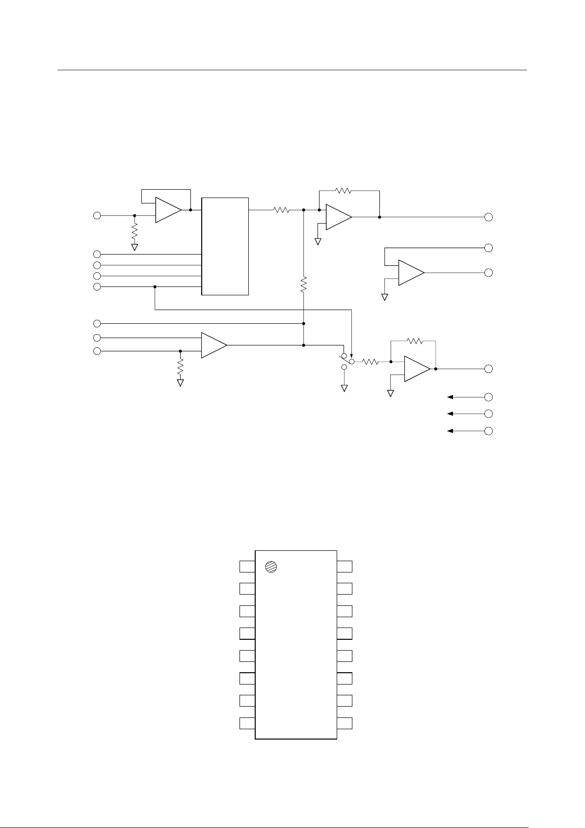
BLOCK DIAGRAM
MSM7577¡ Semiconductor
RAUD
ATT0
ATT1
ATT2
ATTE
AO3
AN3
MIC
200 kW
SG
ATT
56 kW
–
+
io
ATT0
ATT1
ATT2
ATTE
10 kW
–
+
SG
150 kW
RCV1
AN2
–
+
RCV2
SG
–
SG
+
200 kW
35 kW
SG
SG
35 kW
–
+
TAUD
V
DD
GND
PD
PIN CONFIGURATION (TOP VIEW)
TAUD 1
AN2 2
PD 3
RCV2 4
RCV1 5
NC 6
RAUD 7
GND 8
NC : No connect pin
16-Pin Plastic SOP
DD
16 V
15 AO3
14 MIC
13 AN3
12 ATTE
11 ATT2
10 ATT1
9 ATT0
2/8
Page 3
PIN DESCRIPTION
Pin No. Name I/O Description
1
2
3
4
5
6
7
8
TAUD O Output pin of transmitting voice.
AN2 I
PD 1
RCV2 O
RCV1 O
NC — No Connection.
RAUD I Receive voice input.
GND — Ground (0 V).
Receive voice input.
Gain control should be connected by a resistor between AN2 pin RCV2 pin.
Power down control.
H : Power down
L : Power on
Output pin of receiving voice.
Gain control should be connected by a resistor between AN2 and RCV2 pin.
RCV2 signal is opposite phase to RCV1 signal.
Receive voice input.
RCV1 signal is opposite phase to RCV2 signal.
Volume control.
MSM7577¡ Semiconductor
9
10
11
12 ATTE I
13
14
15
16 V
ATT0
ATT1
ATT2
AN3 I
MIC I Input pin of Microphone signal.
AO3 O
DD
ATT2 ATT1 ATT0 Loss level (dB)
0 0 0 0 ±0.3
0 0 1 –2 ±0.3
0 1 0 –4 ±0.3
I
Mute signal input.
H : Mute mode
L : Operating mode
Gain control and frequency responce control.
Gain control should be controlled by a resistor between AN3 and AO3.
Gain control and frequency responce control.
Gain control should be controlled by a resistor between AN3 and AO3.
— Power supply (+3 V).
0 1 1 –7 ±0.3
1 0 0 –10 ±0.3
1 0 1 –13 ±0.3
1 1 0 –16 ±0.3
1 1 1 –19 ±0.3
3/8
Page 4

ABSOLUTE MAXIMUM RATINGS
Parameter Symbol Min. Max. Unit
Power Supply Voltage V
Digital Input Voltage V
Analog Input Voltage V
Storage Temperature T
DD
IND
INA
STG
RECOMMENDED OPERATING CONDITIONS
Parameter Symbol Min. Typ. Max. UnitCondition
Operating Temperature Ta –20 25 70 °C—
Power Supply Voltage V
Analog Output Load
Resistance 1
Analog Output Load
Resistance 2
DD
R
LA1
R
LA2
DD
MSM7577¡ Semiconductor
–0.3 +7.0 V
–0.3 VDD + 0.3 V
–0.3 VDD + 0.3 V
–55 +150 °C
+2.7 +3.00 +5.25 VV
600 — — WTAUD
10——kWExcept TAUD pin.
4/8
Page 5

ELECTRICAL CHARACTERISTICS
MSM7577¡ Semiconductor
DC Characteristics
( Ta = –20°C to 70°C, V
= 2.7 V to 5.25 V )
DD
Parameter Symbol Condition Min. Typ. Max. Unit
Power Supply Current I
Low Level Input
Voltage
High Level Input
Voltage
Digital Input Leakage
Current
Analog Input
Voltage Level
Analog Input
Resistance
Analog Output
Level Range 1
Analog Output
Level Range 2
DD
*VDD = 5.0 V — 10.0 20
PD = V
DD
ATT0 to ATT2
VDD = 3.0 V
V
IL
ATTE, PD
ATT0 to ATT2
V
IH
I
IL
I
IH
ATTE, PD
= GND
V
I
VI = V
DD
RAUD, MIC
V
IA
AN2, AN3
RAUD
R
IA
MIC
RCV1, RCV2, AO3
V
01
= 5 kW (to SG level)
R
L
TAUD
V
02
= 600 W (to SG level)
R
L
— 1.2 2.4
— 0.1 0.2Power Down Current — mA
0.3 ¥
0—
VDD
0.7 ¥
VDD
—V
DD
–10 — +10 mA
— — 1.2 V
— 200 — kW
1.2 — — V
1.2 — — V
mA
V
V
P-P
P-P
P-P
5/8
Page 6

Analog Interface Characteristics
( Ta = –20°C to 70°C, V
Parameter Symbol Condition Min. Typ. Max. Unit
RAUD-RCV1
RX-AUDIO
Path Gain
V
RXA
ATT = 0 dB
ATTE = L
+14 +15 +16 dB
RAUD-RCV1
RX-AUDIO
Loss Level (Mute)
L
RXA
RAUD = –20 dBV
ATTE = 0 dB
40 — — dB
ATTE = LÆH
MIC-TAUD
TX-AUDIO
Loss Level
L
TXA
MIC = –20 dBV
ATTE = LÆH
40 — — dB
MIC-TAUD
TX-AUDIO
Path Gain
V
TXA
AO3 and AN3 are connected
600 W load resistance
–1.0 0 +1.0 dB
MIC-RCV1
MIC Path Gain V
ATT
Establish Error
RTA
AO3 and AN3 are connected
RAUD-RCV1
V
ATG
ATT0 to ATT2
–9.5 –8.5 –7.5 dB
–0.3 0 +0.3 dB
MIC = –7.45 dBV
TX-AUDIO
Distortion
———8%
fi = 1 kHz
600 W load resistance
= 2.7 V to 5.25 V )
DD
MSM7577¡ Semiconductor
6/8
Page 7

APPLICATION CIRCUIT
Transmit voice data
R2
R1
Receive voice data
In the Reverse Type
C1
C3
C6
MSM7577MS-K
TAUD
1
AN2
2
PD
3
RCV2
4
RCV1
5
NC
6
RAUD
7
GND
8
V
DD
AO3
MIC
AN3
ATTE
ATT2
ATT1
ATT0
16
15
14
13
12
11
10
9
MSM7577¡ Semiconductor
+3 V
C2
C4
C1
R1 > 30 kW
R2 > 30 kW
C1 = 0.1 µF
C2 = 1 µF
C3 = 50 pF
C4 = 10 pF
Gain = R2/R1
C5
Analog input
In the Same Phase Type
Analog input
R3
R6
C8
R4
C7
R5
C9
AO3
AN3
MIC
MIC
AN3
AO3
R3 > 10 kW
R4 > 10 kW
–
+
–
+
C5 > 1 µF
C6 = 50 pF
Gain = R4/R3
R5 > 10 kW
R6 > 10 kW
C7 > 0.1 µF
C8 > 1 µF
C9 = 10 pF
Gain = 1 + (R5/R6)
7/8
Page 8

PACKAGE DIMENSIONS
SOP16-P-300-1.27-K
Mirror finish
MSM7577¡ Semiconductor
(Unit : mm)
Package material
Lead frame material
Pin treatment
Solder plate thickness
Package weight (g)
Epoxy resin
Cu alloy
Solder plating
5 mm or more
0.21 TYP.
Notes for Mounting the Surface Mount Type Package
The SOP, QFP, TSOP, SOJ, QFJ (PLCC), SHP and BGA are surface mount type packages, which
are very susceptible to heat in reflow mounting and humidity absorbed in storage.
Therefore, before you perform reflow mounting, contact Oki’s responsible sales person for the
product name, package name, pin number, package code and desired mounting conditions
(reflow method, temperature and times).
8/8
 Loading...