

Page 1

E2U0023-28-81
¡ Semiconductor MSM7502
¡ Semiconductor
This version: Aug. 1998
Previous version: Nov. 1996
MSM7502
Multi-Function PCM CODEC
GENERAL DESCRIPTION
The MSM7502, developed especially for low-power and multi-function applications in touchtone telephone sets and digital telephone terminals of digital PBXs, is a single +5 V power supply
CODEC device. The device consists of the analog speech paths directly connectable to a handset,
the calling circuit directly connectable to a piezosounder, the push-button key scanning interface
between push buttons and control processors, the dial tone generator, the m-law/A-law CODEC,
and the processor interface. The functions can be controlled via 8-bit data bus.
For the CODEC of the MSM7502, an MSM7543 is used as a core CODEC, so the MSM7502
provides the available bit clock range wider than the family product MSM6895.
In addition, the MSM7502 performs the greater key interface function and offers the upgraded
side-tone level, receive level, and speaker pre-amplifier output level.
FEATURES
• Single +5 V Power Supply
• Low Power Dissipation
Power ON Mode : 30 mW Typ. 53 mW Max.
Power Saving Mode : 2 mW Typ. 5 mW Max.
• In compliance with ITU-T’s companding law
• Transmission clocks : 64, 128, 256, 512, 1024, 2048 kHz
96, 192, 384, 768, 1536, 1544 kHz
• Built-in PLL
• Built-in Reference Voltage Supply
• Calling Tone Interval : Controlled by processor
• Calling Tone Combination : Controlled by processor, 6 modes
• Calling Tone Volume : Controlled by processor, 4 modes
• Ringing Tone Interval : Controlled by processor
• Ringing Tone Frequency : Controlled by processor, 6 modes
• Ringing Tone Level : Controlled by processor, 4 levels
• Built-in PB Tone Generator
• Built-in Speech path Control Switches
• General Latch Output for External Control : 2 bits
• Watch-dog Timer : 500 ms
• Key Scanning I/O
Output : 8 bits
Input : 8 bits
• Direct Connection to Handset : 1.2 kW driving available
• Built-in Pre-amplifier for Loud-speaker
• Hand-free Interface
• m-law/A-law Switchable CODEC
• LCD Deflection Angle Voltage : Controlled by processor, 8 levels
• Package :
80-pin plastic QFP (QFP80-P-1420-0.80-BK) (Product name : MSM7502GS-BK)
1/35
Page 2
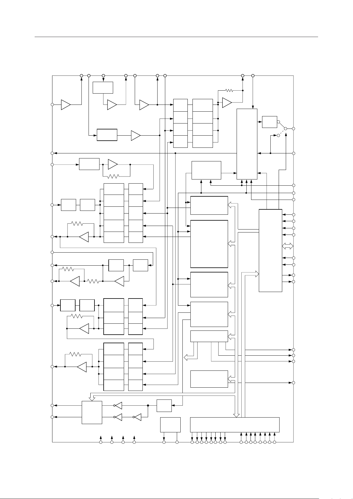
¡ Semiconductor MSM7502
BLOCK DIAGRAM
TPAI
CAO
R1I
R2I
RPO
RMI
RMO0
RMO1
TPAO
20 dB
++–
SW 9 0 dB
0 dB
MPAI MPAO MPBO TOTPBI MPBI MLDYI
VOL 9
VOL 10
–
VOL 8
–
VOL 1
VOL 2
–8.7 dB
0 dB
VOL 7
SW 5 SW 5
+
SW 3
SW 4
SW 17
SW 14
SW 13
––
SW 1
SW 2
SW 7
SW 16
0 dB
5.7 dB
VOL 3
VOL 4
PLL
PB GEN.
R-TONE GEN.
400
425
440
450
400*16
400*20
F-TONE GEN.
1 kHz
CAI
–
AIN
m/A
CODEC
AOUT
SW 12
PROCESSOR INTF
PCMOUT
PCMIN
BCLOCK
XSYNC
RSYNC
WRN
RDN
CEN
RESETN
D0 to D7
AD0
AD1
INTT
TIMEN
SPI
SPO
SA0
SA1
SW 10 VOL 6
–
–
VOL 13
0 dB
–3 dB
–6.8 dB
VOL 5
–22 dB
VOL 11
VOL 12
VA VD AG DG SGT SGC PO0 to PO7 PI0 to PI7
SW 6
SW 8
SW 18
SW 21
SW 15
SW 11
SW 20
SW 19
SG GEN.
S-TONE GEN.
WAMBLE TONE
1000 Hz
800 Hz
400 Hz
Latch
VLCD GEN.
KEY INTF
SCANNING OUTPUT SCANNING INPUT
LA
LB
LML
VLCD
2/35
Page 3
¡ Semiconductor MSM7502
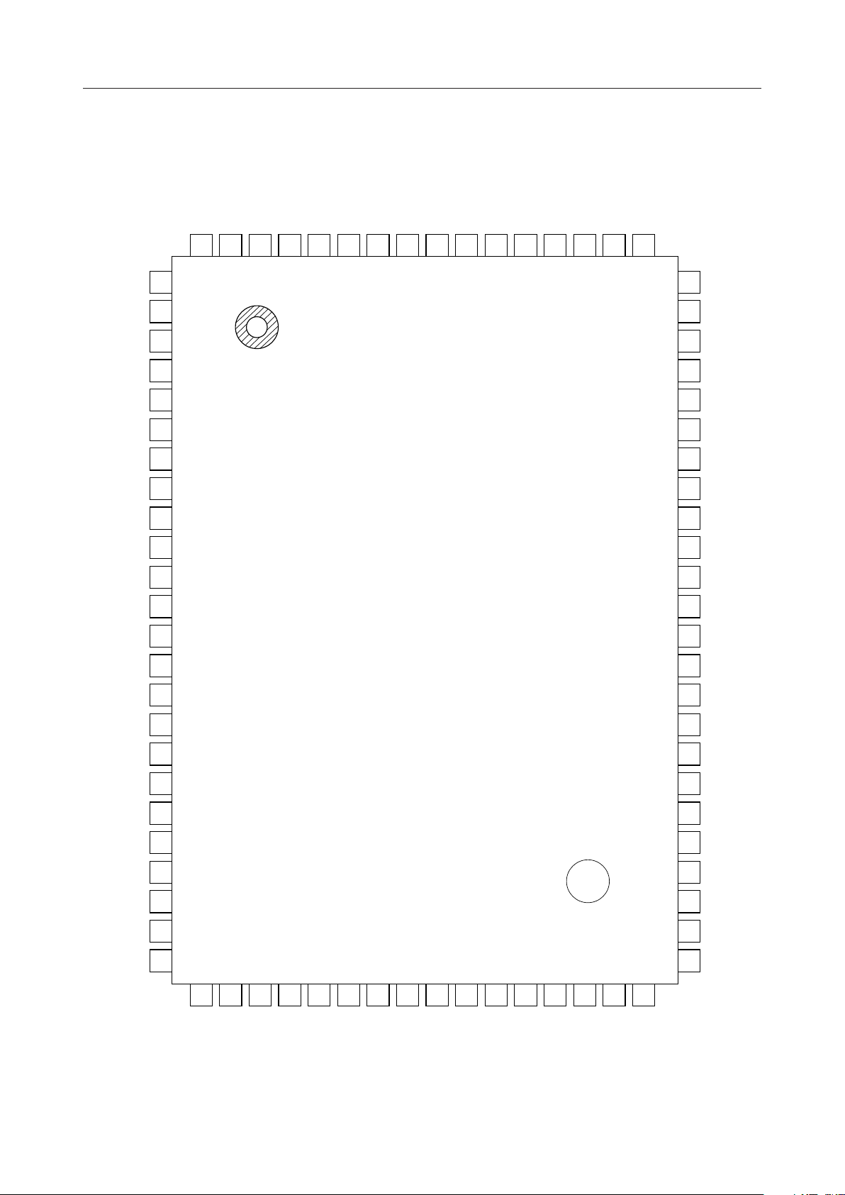
PIN CONFIGURATION (TOP VIEW)
TIMEN
INTT
80
79
RESETN
78
CEN
77
RDN
76
WRN
75
AD1
74
AD0
73
DB7
72
DB6
71
DB5
70
DB4
69
DB3
68
DB2
67
DB1
66
DB0
65
LML
LA
LB
VLCD
SA1
SA0
DG
AG
RMO1
RMO0
RMI
SPI
NC
SPO
10
11
12
13
14
1
2
3
4
5
6
7
8
9
64
63
62
61
60
59
58
57
56
55
54
53
52
51
VD
PI7
PI6
PI5
PI4
PI3
PI2
PI1
PI0
NC
PO0
PO1
PO2
PO3
RPO
R2I
R1I
MLDYI
MPBO
MPBI
MPAO
NC
MPAI
NC
15
16
17
18
19
20
21
22
23
24
25
NC
26
TPBI
27
TPAO
28
NC
29
30
31
32
TO
SGT
TPAI
NC : No connect pin
80-Pin Plastic QFP
VA
33
NC
34
CAI
35
NC
36
SGC
37
NC
38
NC
39
CAO
40
NC
50
49
48
47
46
45
44
43
42
41
PO4
PO5
PO6
PO7
PCMOUT
BCLOCK
XSYNC
RSYNC
PCMIN
NC
3/35
Page 4

¡ Semiconductor MSM7502
PIN AND FUNCTIONAL DESCRIPTIONS
LA, LB
General latch outputs for external control.
Statuses of these outputs are controlled via the processor interface. Refer to the description of the
control data for details. These outputs provide the capability to drive one TTL.
DG
Digital Ground.
DG is separated from the analog ground AG inside the device. But, DG should be connected as
close to the AG pin on PCB as possible.
AG
Analog Ground.
SA0, SA1
Sounder (calling tone) driving outputs.
The output signal on SA1 is inverted against the signal on SA0. The sounder circuit can be easily
configured by connecting a piezo-sounder between SA0 and SA1. Through processor control, the
calling tone volume is selectable from four levels and one of six tone combinations is selectable.
Initially, the ringing tone volume is set at a maximum and the tone combination is set at a 16 Hz
Wamble tone by a combination of 1 kHz and 1.3 kHz. If these pins are used with no-load, tone
volume cannot be controlled. When tone volume control is required, a load resistor must be
connected between SA0 and SA1.
4/35
Page 5
¡ Semiconductor MSM7502
RMI, RMO0, RMO1
Receive main amplifier input and outputs.
RMI is the inverted input and RMO0 and RMO1 are the outputs of the receive main amplifier.
The output signal on RMO1 is inverted against RMO0 by a gain 1 (0 dB), so the earphone of a
handset is directly connected between RMO0 and RMO1. During the system power down, the
RMO0 and RMO1 outputs are in a high impedance state. The receive main amplifier gain is
determined by a resistor connected between RPO and RMI, and a resistor connected between
RMI and RMO0. The receive main amplifier gain varies between 0 and +20 dB in effect. A piezoreceiver with an impedance greater than 1.2 kW is available.
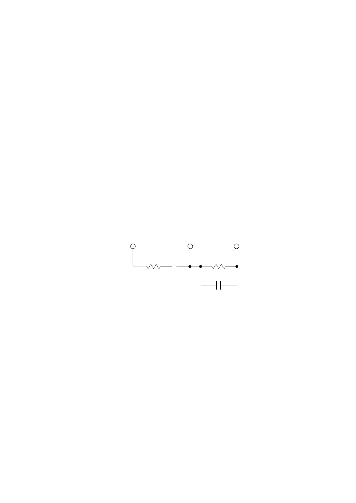
If the adjusting of receive path frequency characteristics is required, insert the following circuit
for adjustment. During the whole system Power ON, the speech path from RMI to RMO0 and
RMO1 is disconnected and the output of RMO0 and RMO1 is at the SG level (VA/2). The speech
path is provided by processor control.
A circuit example for adjustment of frequency characteristics
RPO RMI
R1
Main amplifier gain without capacitors
C1 R2
RMO0
C2
G=
R2
R1
5/35
Page 6

¡ Semiconductor MSM7502
SPI
Addit0ion input of speaker amplifier.
The typical gain between SPI and SPO is 0 dB. But, the 2-stage gain amplifier allows to set up a
gain between 0 dB and –18 dB in a 6 dB step, or a gain between 0 dB and –28 dB in a 4 dB step
through processor control. The input resistance of SPI is typically 20 kW to 150 kW (it varies by
gain setting).
SPO
Output of pre-amplifier for speaker.
Since the driving capability is 2.4 VPP for the load of 20 kW, SPO can not directly drive a speaker.
During the whole system power down mode, SPO is at an analog ground level. During the whole
system power on mode, SPO is in a non-signal state (SG level), and a receive voice signal, R-tone,
F-tone, hold acknowledge tone, PB signal acknowledge tone, and sounder tone are output from
the speaker by processor control.
When the speaker is used as a sounder, the sounder tone is output via the SPO pin by connecting
the SPI input with the sounder output (SA0 or SA1). In addition, when the AD-converted
sounder tone is sent from the main device, the sounder tone is output via the SPO pin since the
CAO pin for CODEC output is internally connected.
R1I, R2I, RPO
R1I and R2I are for the inputs and RPO is for the output of the receive pre-amplifier.
Normally, R1I is connected via an AC-coupling capacitor to the CODEC analog output (CAO),
and R2I is used as the mixing signal input pin.
The typical gain between R1I and PRO is –6 dB. Through processor control, gains are variable
from –14 dB to 0 dB in 2 dB steps. In addition, the receive pad can control the gain of –9, –6, –3,
or 0 dB. The gain between R2I and RPO is fixed to 0 dB.
During the whole system power-on mode, the RPO output is in non-signal state, and speech
signal, R-tone, F-tone, PB acknowledge tone, side tone signal are output by processor control.
During the whole system power-down mode, the RPO output is the analog ground level.
The input resistance of R1I is typically between 20 kW and 100 kW (it varies by gain setting). The
input resistance of R2I is typically 20 kW.
MLDYI
Hold tone signal input.
For example, the output of external melody IC is connected to this pin. Through processor
control, the signal applied to MLDYI is output from the TO output pin as a hold tone on the
transmit path, and from the SPO output pin as a hold acknowledge tone on the receive path. The
typical gain between MLDYI and TO is –2 dB. Through processor control, a gain between –2 dB
and –11 dB is also settable at 3 dB steps. The typical gain between MLDYI and SPO is –3 dB.
Through processor control, a gain between –3 dB to –31 dB is also settable at 4 dB steps. MLDYI
is a high impedance input, so insert an about 100 kW bias resistor between MLDYI and SGT.
6/35
Page 7
¡ Semiconductor MSM7502
TPBI, TO
TPBI is the input and TO is the output of the transmit pre-amplifier (B).
When the handset is used, TPBI is connected to the transmit pre-amplifier (A) output pin (TPAO).
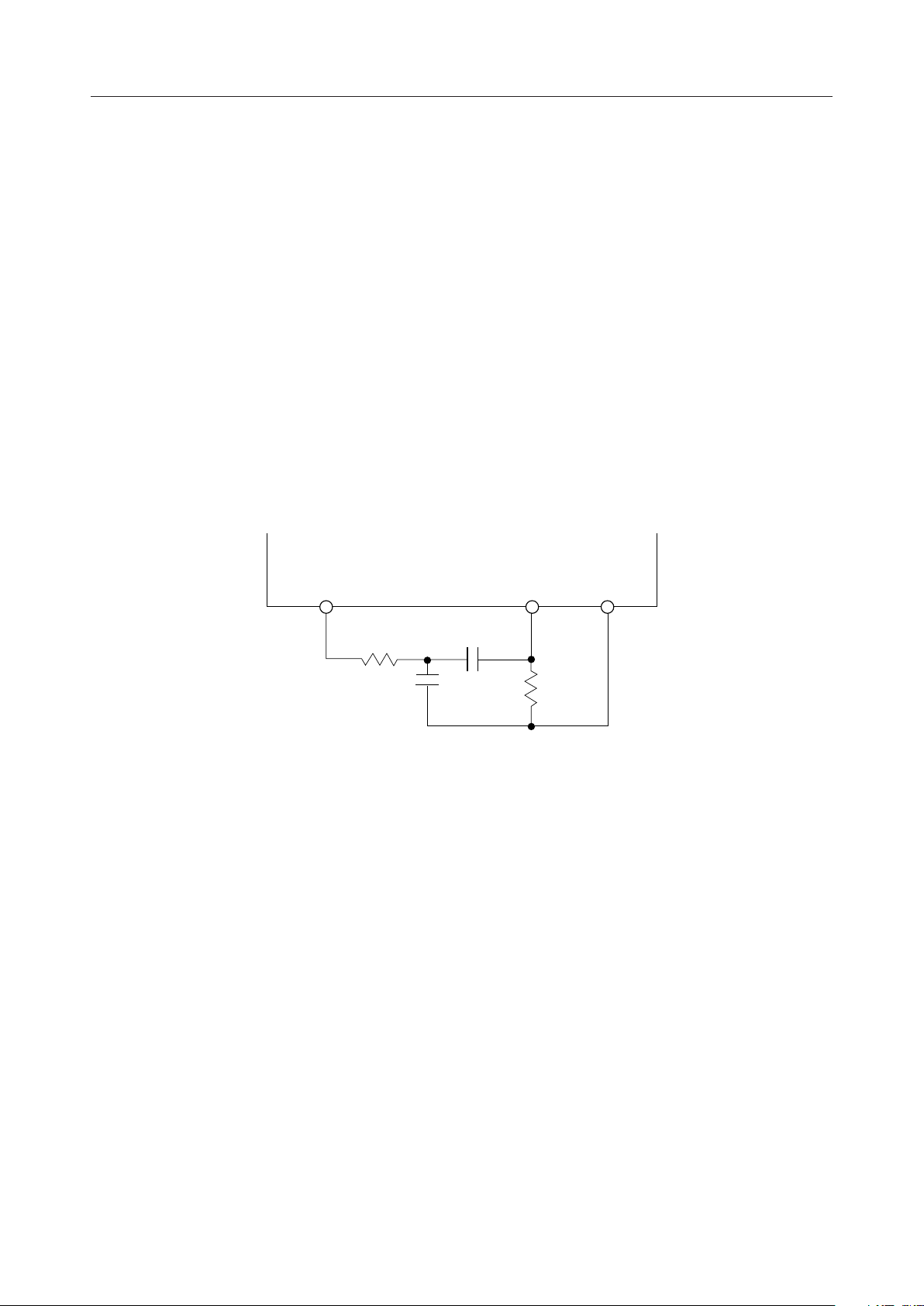
If adjustment of frequency characteristics on the transmit path is required, insert a circuit for
adjustment of characteristic between TPAO and TPBI. Through processor control, the signal
applied to this pin is output via the TO pin on the transmit path and its side tone via the RPO pin.
During the whole system power down mode, TO is at an analog ground level. The typical gain
between TPBI and TO is +17.7 dB. Through processor control, a gain between +17.7 dB and +8.7
dB is also settable at 3 dB steps.
The typical gain between TPBI and RPO is +3.0 dB. Through processor control, a gain between
–9 dB and +9 dB is variable in 3 dB steps. Changing the gain between TPBI and TO may change
the gain between TPBI and RPO. TPBI is a high impedance input, so insert an about 100 kW
resistor between TPBI and SGT.
A circuit example for adjustment of frequency characteristics
TPAO TPBI SGT
C3R3
R4
C4
MPAI, MPAO
Handfree microphone pre-amplifier (A) input and output.
MPAI is the input and MPAO is the output. The speech path between MPAI and MPAO is always
active regardless of processor control. During the whole system power saving mode, MPAO is
at an analog ground level. The gain between MPAI and MPAO is typically +20 dB. Through
processor control, gains between +14 dB and +11 dB are also settable. MPAI is a high impedance
input, so insert an about 100 kW between MPAI and SGT.
MPBI, MPBO
The handfree microphone (B) input and output.
MPBI is the inverted input and MPBO is the output. With an external resistance, the amplifier
gain is adjusted in the range between –25 dB and +25 dB. A signal on the MPBO is output via the
TO pin through processor control. During the whole system power down mode, MPBO is at an
analog ground level. The gain between MPBO and TO is fixed to 0 dB.
7/35
Page 8

¡ Semiconductor MSM7502
TPAI, TPAO
The transmit pre-amplifier input and output.
TPAI is the input and TPAO is the output. TPAI should be connected to the microphone of
handset via an AC-coupling capacitor if the DC offset appears at a transmit signal (offset from
SGT). The transmit path from TPAI to TPAO is always active regardless of processor control.
During the whole system power down mode, TPAO is at an analog ground level. The gain
between TPAI and TPAO is fixed to 20 dB.
SGT
Transmit path signal ground.
SGT outputs half the supply voltage. During the whole power down mode, SGT is in a high
impedance state.
SGC
Bypass capacitor connecting pin for signal ground level.
Insert a 0.1 mF high performance capacitor between SGC and AG.
VA, VD
+5 V power supply.
VA is for an analog circuit and VD is for digital supply. Connect both VA and VD to the +5 V
analog path of the system.
CAI, CAO
CODEC analog input and output.
CAI is the analog input of CODEC to be connected to the TO pin. If the DC offset voltage on the
TO signal is great, CAI should be connected via AC-coupling capacitor. At this time, insert an
about 100 kW bias resistor between CAI and SGT.
CAO is the analog output of CODEC. CAO should be connected to R1I via AC-coupling
capacitor. A bias resistor is not required to R1I. During the whole system or CODEC power down
mode, CAO is at the SG voltage level.
8/35
Page 9

¡ Semiconductor MSM7502
BCLOCK
CODEC PCM data I/O shift clock input.
The frequency is one of 64 kHz, 128 kHz, 256 kHz, 512 kHz, 1024 kHz, 2048 kHz, 96 kHz, 192 kHz,
384 kHz, 786 kHz, 1536 kHz, and 1544 kHz. If the BCLOCK signal is not applied, PLL is out of
synchronization and the CODEC path goes into the power down mode.
XSYNC, RSYNC
Synchronous signal input.
CODEC PCM data is sent out sequencially via the PCMOUT pin from MSB at the rising edge of
the BCLOCK signal in synchronization with the rise of the XSYNC signal. PCM data should be
entered via the PCMIN pin with MSB at the head in synchronization with the rise of the RSYNC
signal. PCM data is shifted in at the falling edge of the BCLOCK signal.
Since the XSYNC signal is used for a trigger signal for PLL and for a clock signal to the tone
generator, if this signal is not applied, not only any tone can not be output, but also PLL goes out
of synchronization and the CODEC path goes into a power down mode. This signal has to be
synchronous with the BCLOCK signal and its frequency must be within 8 kHz ±50 ppm to ensure
the CODEC AC characteristics (mainly frequency characteristics).
PCMIN
PCM signal input.
PCMIN data is shifted in at the falling edge of the BCLOCK signal and is latched into the internal
register after eight bits are shifted.
PCMOUT
PCM signal output.
PCMOUT data is shifted out at the rising edge of the BCLOCK signal. PCMOUT is left open after
eight bits are shifted or when PLL goes out of synchronization. PCMOUT also is left open
through processor control. In addition, a digital path between PCMIN and PCMOUT is formed
through processor control. PCMOUT needs a pull-up resistor because of its open-drain circuit.
9/35
Page 10
¡ Semiconductor MSM7502
PO0, PO1, PO2, PO3, PO4, PO5, PO6, PO7
Key scanning outputs.
These output pins need external pull-up resistors because of their open- drain circuits. But, when
these are used in combination with PI0 to PI7, pull-up resistors are not required. Through
processor control, these outputs can be set open or to digital "0". Initially, these outputs are set
at an opened state.
PI0, PI1, PI2, PI3, PI4, PI5, PI6, PI7
Key scanning inputs.
In the READ mode, data on PI0 to PI7 can be read out of the processor via data bus (DB0 to DB7).
Since these inputs are pulled up inside the IC, external resistors are not required.
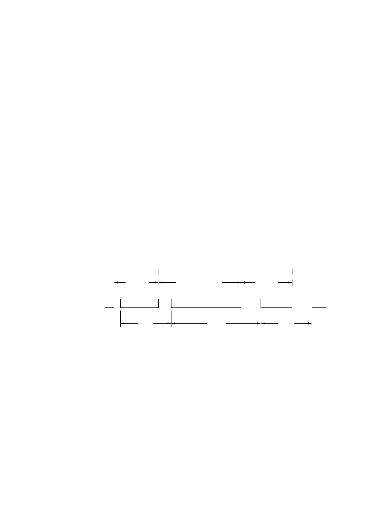
INTT
Interrupt signal output to the processor.
INTT outputs interrupt signals (digital "0") at intervals of 8 ms by the interrupt release control
signal from the processor. This output keeps digital "0" unless the interrupt is released. INTT
does not output any signal while no XSYNC signal is input. When the RESETN signal is in "0"
state, INTT is in "1" state. INTT goes from "1" state to "0" state 8 ms after the RESETN signal goes
to "1" state.
Interrupt release signal
from processor
INTT output
t < 8 ms 8 ms < t < 16 ms t < 8 ms
8 ms 16 ms 8 ms
DB0, DB1, DB2, DB3, DB4, DB5, DB6, DB7
Data bus inputs and outputs.
These pins are configured as an output during the READ mode only and as an input during other
modes.
10/35
Page 11

¡ Semiconductor MSM7502
AD0, AD1
Address data inputs for the internal control registers.
Addressing of the internal control registers is executed by AD0 and AD1 and sub address data,
DB7 and DB6.
AD1 AD0 DB7 DB6 Function
0 0 ON/OFF controls of sounder, R-Tone, F-Tone
0 1 Level/Frequency controls of sounder, R-Tone
WRITE
00
01
1 0 — — Key scanning output control
1 1 0 0 Key scanning interrupt reset
1 1 0 1 LCD deflection angle control voltage setting
1 1 1 0 Power ON/OFF control
1 1 1 1 CODEC control (Controls of companding law and digital loop)
1 0 PB tone control
11
0 0 Controls of receive gain and side tone gain
0 1 Controls of transmit hold tone, PB tone, handfree input, handset inputs gain
1 0 Controls of speaker pre-amplifier gain and additional speaker gain
1 1 Controls of receive PAD and incoming tone input gain
Controls of internal speech path switch and general latch
Watchdog timer reset
READ
1 0 — — Key scanning data read-out
WRN
Write signal for internal control registers.
Data on the data bus is written into the registers at the rising edge of WRN under the condition
of digital "0" of CEN (Chip Enable). While CEN is in digital "1" state, WRN becomes invalid. The
Write cycle is a minimum of 2 ms regardless of the presence or absence of clock signals.
RDN
Read signal input to read PI0 to PI7 out of the processor.
When CEN and RDN are in digital "0" state, the digital values on PI0 to PI7 are output onto the
data buses DB0 to DB7. While CEN is in digital "1" state, the RDN signal becomes invalid.
11/35
Page 12

¡ Semiconductor MSM7502
CEN
Chip Enable signal input.
When CEN is in digital "0" state, WRN and RDN are valid.
RESETN
Reset signal input.
Digital "0" input to RESETN makes all of internal control registers to be initialized. When
powered on, this RESETN signal should be input for initializing the system.
TIMEN
Watchdog timer output.
When the processor does not reset the timer, the 500 ms period (Digital "0" : 4 ms) digital signal
is continuously output. When RESETN is at digital "0", this timer is reset. And, in about 500 ms
after RESETN goes to digital "1", the first timer output signal is issued and then the timer signal
is output at intervals of a 500 ms. If the SYNC signal is not input, the TIMEN signal is not output.
LML
Control signal output for external hold tone generator.
LML goes to digital "1" state when the hold tone transmit mode on transmit path or the hold
acknowledge tone mode on receive path is selected. During initialized state, LML is in digital "0"
state.
VLCD
By processor control, VLCD outputs a DC voltage between 0 and 1.7 V is about 0.25 V step.
This is used to control the deflection angle of the LCD display. VLCD has the internal resistance
value of about 1 kW, so the external load of over 100 kW should be used. During initialized state,
VLCD outputs the voltage of 0 V.
12/35
Page 13
¡ Semiconductor MSM7502
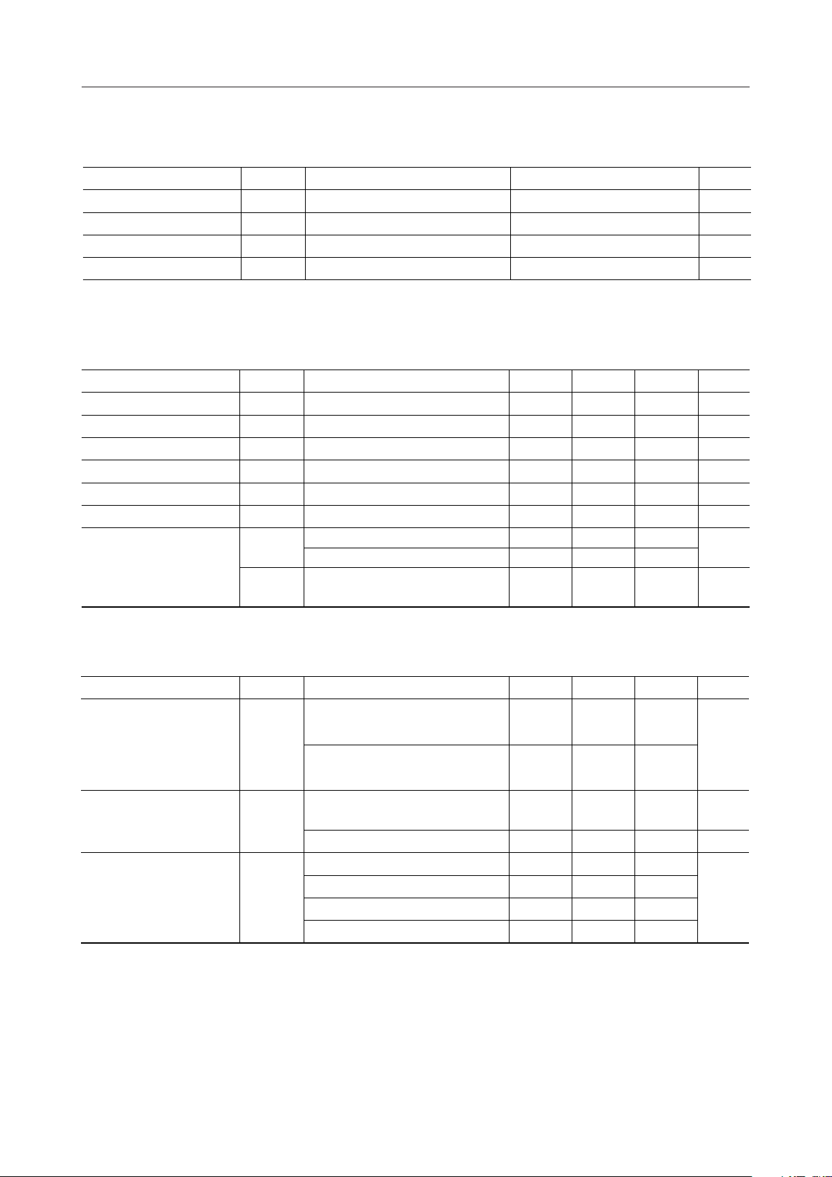
ABSOLUTE MAXIMUM RATINGS
Parameter Symbol Condition Rating Unit
Power Supply Voltage V
Digital Input Voltage V
Storage Temperature T
DD
AIN
DIN
STG
AG, DG = 0 V
AG, DG = 0 V
AG, DG = 0 V
—
0 to 7
-0.3 to V
-0.3 to V
-55 to +150
DD
DD
+ 0.3
+ 0.3
V
VAnalog Input Voltage V
V
°C
RECOMMENDED OPERATING CONDITIONS
Min. Max.Parameter Symbol Condition Typ. Unit
Power Supply Voltage V
Operating Temperature °C
Input High Voltage
Input Low Voltage V
Digital Input Rise Time t
Digital Input Fall Time t
V
D
Ta — +25–10 +70
V
IH
IL
Ir
If
R
DL
Digital Output Load
C
DL
VA, VD (Voltage must be fixed) 5.04.75 5.25
All Digital Input Pins —2.2 V
DD
V
All Digital Input Pins —0 0.8 V
All Digital Input Pins ——50ns
All Digital Input Pins ——50ns
PO0 to PO7
PCMOUT
PO0 to PO7
PCMOUT
10
0.5
—
—
——
—
—
100
kW
pF
Recommend Operating Conditions (Analog Interface)
Min. Max.Parameter Symbol Condition Typ. Unit
TPAO, MPAO, MPBO, TO,
RPO, SPO, CAO
Analog Load Resistance kW
R
AL
RMO0, RMO1 with respected to
SG Level
TPAO, MPAO, MPBO, TO,
Analog Load Capacitance
C
RPO, SPO, CAO
AL
RMO0, RMO1 ——70
TPAI, TPBI, MPAI —–10 +10
Allowable Analog
Input Offset Voltage
V
MLDY —–50 +50
off
R1I, R2I, SPI —–25 +25
CAI —–100 +100
—20 —
—0.6 —
—— 100
mV
pF
nF
13/35
Page 14
¡ Semiconductor MSM7502
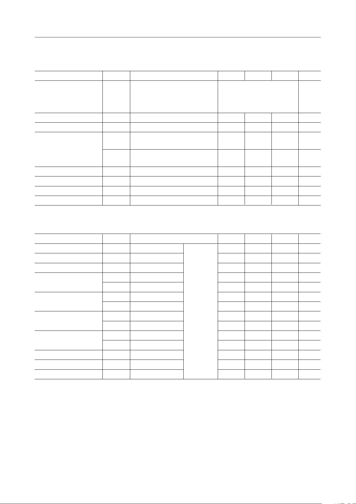
Recommended Operating Conditions (CODEC Digital Interface)
Min. Max.Parameter Symbol Condition Typ. Unit
64, 128, 256, 512, 1024,
Clock Frequency kHz
Sync Pulse Frequency
Clock Duty Ratio
F
C
F
S
D
C
t
XS
Sync Pulse Setting Time
t
SX
Sync Pulse Width t
Data Setup Time
Data Hold Time t
WS
t
DS
DH
BCLOCK
XSYNC, RSYNC
BCLOCK
BCLOCKÆX, RSYNC
See Fig.1
X, RSYNCÆBCLOCK
See Fig.1
XSYNC, RSYNC —1 BCK 100
PCMIN —100 — ns
PCMIN —100 — ns
Allowable Jitter Width — XSYNC, RSYNC —— 500 ns
2048
96, 192, 384, 768, 1536,
1544
8.06.0 10.0
5040 60 %
—— 100 ns
—— 100 ns
kHz
m
s
Recommended Operating Conditions (Processor Digital Interface)
Min. Max.Parameter Symbol Condition Typ. Unit
Write Pulse Period nsWRN —2000 —
Write Pulse Width nsWRN —100 —
Read Pulse Width nsRDN —200 —
Address Data
Setup Time
Address Data
Hold Time
CEN Setup Time
CEN Hold Time
Data Setup Time ns—110 —t
P
W
T
W
T
R
AW1
AR1
AW2
AR2
CW1
CR1
CW2
CR2
DW1
DW2
WRES
AD0, AD1ÆWRN
AD0, AD1ÆRDN ns—80 —t
WRNÆAD0, AD1
RDNÆAD0, AD1 ns—10 —t
CENÆWRN
CENÆRDN ns—80 —t
WRNÆCEN
RDNÆCEN ns—10 —t
DB0 to 7ÆWRN
WRNÆDB0 to 7Data Hold Time ns—20 —t
RESETNReset Pulse Width ns—110 —t
See Fig.2
ns—10 —t
ns—50 —t
ns—10 —t
ns—50 —t
14/35
Page 15
¡ Semiconductor MSM7502
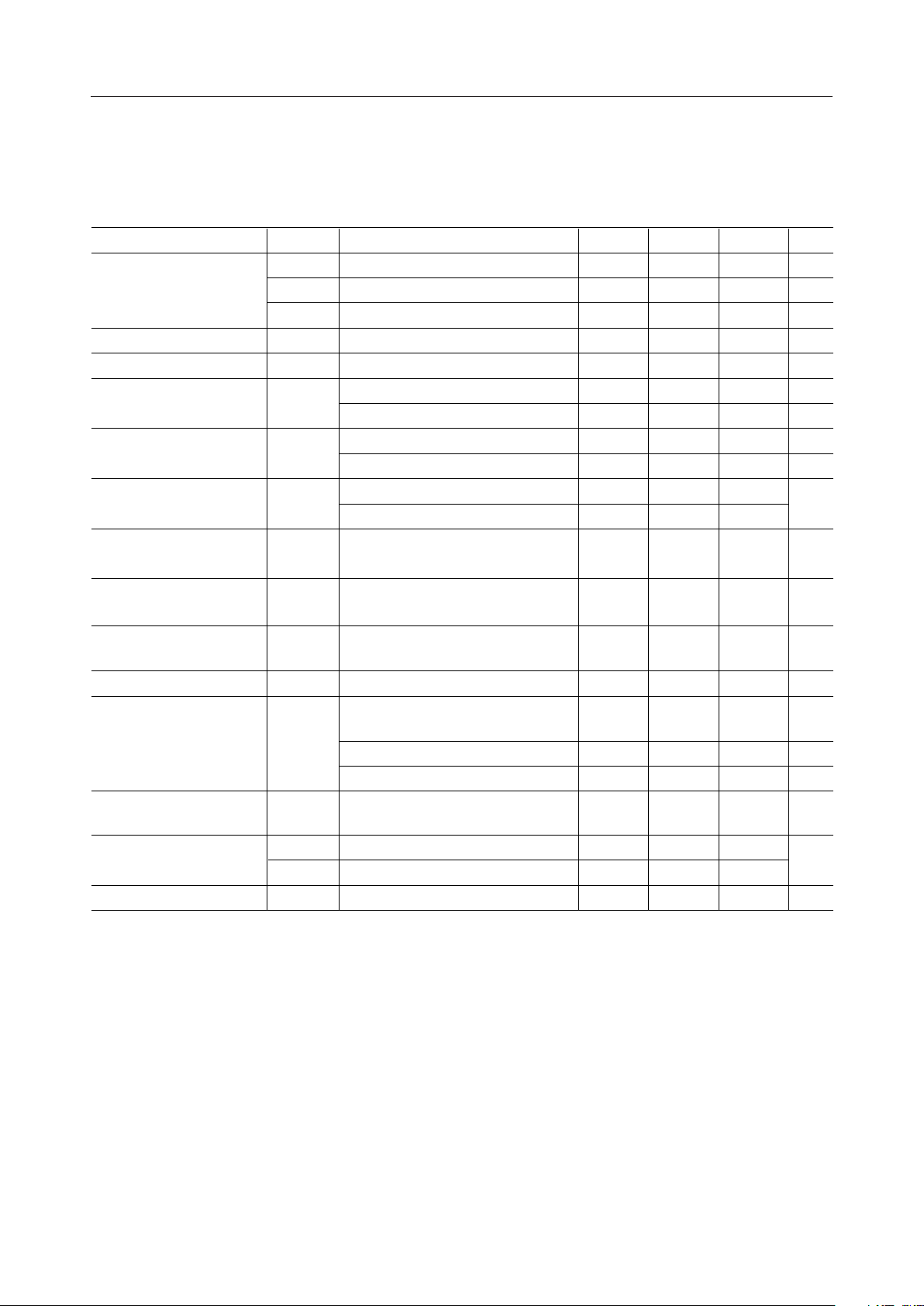
ELECTRICAL CHARACTERISTICS
DC and Digital Interface Characteristics
= 5 V ±5%, Ta = –10°C to +70°C)
(V
DD
Min. Max.Parameter Symbol Condition Typ. Unit
I
Power Supply Current
I
I
Input High Voltage V
Input Low Voltage V
High Input Leakage
Current
Low Input Leakage
Current
Digital Output High
Voltage
V
Digital Output Low
Voltage
DD1
DD2
DD3
I
I
V
IH
IL
IH
IL
OH
OL
Operating Mode (No Signal, Sounder OFF)
6.0— 10.0
Whole system Power Down 0.4— 0.8 mA
CODEC Power Down 2.8— 5.0 mA
——2.2 V
DD
——0.0 0.8 V
Digital Pins except for PI0 to PI7 —— 2.0 mA
PI0 to PI7 (Internal Pull-up Pins) —— 2.0 mA
Digital Pins except for PI0 to PI7 —— 0.5 mA
PI0 to PI7 (Internal Pull-up Pins) —10 25 mA
I
= 0.4 mA
OH
IOH = 1 mA
I
= –1.6 mA 0.0
OL
2.4
3.8
—
—
V
DD
V
DD
— 0.4 V
mA
V
V
Digital Output Leakage
Current
Analog Output Offset
Voltage
Input Capacitance C
I
O
V
off
IN
PCMOUT, DB0 to DB7
(Write Mode)
TPAO, MPAO, MPBO, TO,
CAO, RPO, RMO0, RMO1, SPO
—5——pF
——10mA
—–100 +100 mV
TPAI, TPBI, MLDYI, RMI, MPAI,
10——MW
Analog Input Resistance R
MPBI
IN
R1I, R2I, SPI —10 — kW
CAI (fin : < 4 kHz) 1——MW
SG Voltage — — VA/2 V
I
R
SGF
I
SGS
PULL
SG Drive Current mA
Equivalent Pull-up Resistance
FORCE Current 1.51.0 —
SINK Current 0.50.3 —
PI0 to PI7, VI = 0 V 370200 500 kW
VA/2
–0.05
VA/2
+0.05
15/35
Page 16

¡ Semiconductor MSM7502
AC Characteristics 1 (CODEC)
(VDD = 5 V ±5%, Ta = –10°C to +70°C)
Parameter Symbol Condition Typ. UnitMin. Max.
Loss T1
Loss T2
Transmit Frequency
Response
Receive Frequency
Response
Transmit Signal to
Distortion Ratio
Receive Signal to
Distortion Ratio
Transmit Gain
Tracking
Receive Gain
Tracking
Loss T3
Loss T4
Loss T5
Loss T6
Loss R1
Loss R2
Loss R3
Loss R4
Loss R5
SD T1
SD T2
SD T3
SD T4
SD T5
SD R1
SD R2
SD R3
SD R4
SD R5
GT T1
GT T2
GT T3
GT T4
GT T5
GT R1
GT R2
GT R3
GT R4
GT R5
Freq.
(Hz)
300
1020
2020
3000
3400
300
1020
2020
3000
3400
1020
1020
1020
1020
60
Level
(dBm0)
0
3
0
–30
–40
–45
3
0
–30
–40
–45
3
–10
–40
–50
–55
3
–10
–40
–50
–55
*1
*1
20
–0.20
–0.15
–0.15
0.0
–0.15
–0.15
–0.15
0.0
35
35
35
29
24
37
37
37
30
25
–0.2
–0.2
–0.4
–1.2
–0.2
–0.2
–0.5
–1.2
+0.07
Reference
–0.03
+0.06
0.38
–0.03
Reference
–0.02
+0.15
0.56
43.0
41.0
38.0
31.0
26.5
43.0
41.0
40.0
34.0
31.0
+0.01
Reference
–0.05
+0.05
+0.30
Reference
–0.10
–0.30
–0.40
27
0.0
—
+0.20
+0.20
+0.20
0.80
+0.20
+0.20
+0.20
0.80
—
—
—
—
—
—
—
—
—
—
+0.2
+0.2
+0.4
+1.2
+0.2
+0.2
+0.5
+1.2
dB
dB0
dB
dB
dB
dB
Note: *1 Psophometric filter is used
16/35
Page 17
¡ Semiconductor MSM7502
AC Characteristics 1 (CODEC) (Continued)
= 5 V ±5%, Ta = –10°C to +70°C)
(V
DD
S
Freq.
(Hz)
1020 0 Vrms
500
600
1000
2600
2800
500
600
1000
2600
2800
1020 0
4.6 kHz to
72 kHz
300 to
3400
fa = 470
fb = 320
0 to 50
kHz50mV
Parameter Symbol Condition Typ. UnitMin. Max.
Nidle T ———
Idle Channel Noise
Nidle R —— — –78.0 –75
Absolute Amplitude
Absolute Delay Time
Transmit Group Delay
Receive Group Delay
Crosstalk Attenuation
Discrimination
Out-of-band Signal
Spurious
Intermodulation Distortion
Power Supply Noise
Rejection Ratio
AV T 0.5671 0.6007 0.6363
AV R 0.5671 0.6007 0.6363
Td 1020 0 — 0.58 0.60 ms
tgd T1
tgd T2
tgd T3
tgd T4
tgd T5
tgd R1
tgd R2
tgd R3
tgd R4
tgd R5
CR T
CR R
DIS
IMD
PSR T
PSR R
Level
(dBm0)
AIN = SG
*1
*1
*3
A to A
BCLOCK = 64 kHz
0*4
0*4
Transmit Æ Receive
Receive Æ Transmit
–25 32.030 — dB
0 –37.5— –35 dBmO
–4 –52— –35 dBmO
pp
0 to 4000 Hz
4.6 kHz to 100 kHz
2fa–fb
*2
—
—
—
—
—
—
—
—
—
—
*5 30——
–73.5
0.19
0.12
0.02
0.05
0.08
0.09
0.12
–71
0.75
0.35
0.125
0.125
0.75
0.0
0.0
0.0
7870 —
8675 —
0.75
0.35
0.125
0.125
0.75
–70
–69
dBmOp
ms
ms
dB
dB
Notes: *2 Upper is specified for the m-law, lower of the A-law
*3 PCMIN input : idle CODE
*4 Minimum value of the group delay distortion
*5 The measurement under idle channel noise
17/35
Page 18
¡ Semiconductor MSM7502
AC Characteristics 2 (Transmit Path)
(V
= 5 V ±5%, Ta = –10°C to +70°C)
DD
Parameter Symbol Condition Typ. UnitMin. Max.
Freq.
(Hz)
GTPAPre-Amp Gain dB
GTPB1Transmit Path Gain dB17.715.7 19.7
1020
Transmit Path Gain
Setting (VOL8)
Microphone Pre-Amp
Gain
Microphone Pre-Amp
RG1TPB
RG2TPB
RG3TPB
GMPA dB20.018.0 22.0
RG1MPA
1020 –24.0
Gain Setting
(VOL9)
Additional Transmit
Signal Gain
In-Channel PB Signal
Output Level
In-Channel PB Signal
Output Level Setting
(VOL4)
In-Channel PB Signal
Frequency Deviation
RG2MPA
GTMX 1020 –4.0 MPBO-TO 0.0–2.0 +2.0 dB
VPBT1 — — –17.4–19.4 –15.4 dBV
GPBT1
GPBT2
GPBT3
DfPBT — — —–1.0 +1.0 %
Level
(dBV)
–24.0
Set at typical gain
Set at typical gain
——
TPBI-TO
For
typical
setting
–3 dB
–6 dB
–9 dB
MPAI-MPAO
For
–6 dB
typical
setting
–9 dB
To per wave
set at typical gain
For
typical
setting
–3 dB
–6 dB
–9 dB
–5.0
–8.0
–11.0
–8.0
–11.0
–5.0
–8.0
–11.0
20.018.0 22.0TPAI-TPAO
–3.0
–6.0
–9.0
–6.0
–9.0
–3.0
–6.0
–9.0
–1.0
–4.0
–7.0
–4.0
–7.0
–1.0
–4.0
–7.0
dB
dB
dB
In-Channel PB Signal
Distortion
THDPBT — — In-band Distortion –35— –30 dB
MLDYI-TO
Hold Tone Path Gain GPAT
Hold Tone Path Gain
Setting
(VOL3)
RG1PAT
RG2PAT
RG3PAT
1020 –4.0
Set at typical gain
For
typical
setting
–3 dB
–6 dB
–9 dB
–5.0
–8.0
–11.0
–2.0–4.0 0.0 dB
–3.0
–6.0
–9.0
–1.0
–4.0
–7.0
dB
TPAI:Terminated in 510 W
Measured at TO
Idle Channel Noise NiTPA — — –75— — dBV
TPAO-TPBI Directly
connected Set at
typical gain *6
TPAO, TO,
Maximum Output Voltage
Swing
VOT 1020 — —2.4 — V
MPAO, MPBO
= 20 kW
R
L
Note: *6 Noise band width: 0.3 kHz to 3.4 kHz, non-weighted
PP
18/35
Page 19
¡ Semiconductor MSM7502
AC Characteristics 3 (Receive Main Amp.)
= 5 V ±5%, Ta = –10°C to +70°C)
(V
DD
Parameter Symbol Condition Typ. UnitMin. Max.
Receive Main Amp
Output Gain Difference
Receive Main Amp
Output Phase Difference
Freq.
(Hz)
DGRMO
DPRMO
Level
(dBV)
RMO0/RMO1
Gain = 1
deg1020 –4.4 –179.6——RMO0/RMO1
1.2 kW between
Maximum Amplitude
VRMO V
1020 — —3.6 —
RMO0 and RMO1.
Measured at each output
AC Characteristics 3 (Receive Path)
= 5 V ±5%, Ta = –10°C to +70°C)
(V
DD
Parameter Symbol Condition Typ. UnitMin. Max.
Freq.
(Hz)
Receive Signal Path Gain dB
GRPA
RGRPA1
RGRPA2
Receive Signal
Path Gain Setting
(VOL1)
RGRPA3
RGRPA4
RGRPA5
1020
RGRPA6
RGRPA7
Receive PAD
Gain Setting
(VOL10)
RGPAD1
RGPAD2
RGPAD3
Level
(dBV)
–4.0
Typical gain is set
between R1I and RPO
–8 dB
–6 dB
For
typical
setting
–4 dB
–2 dB
2 dB
4 dB
6 dB
For
typical
setting
–3 dB
–6 dB
–9 dB
–10.0
–8.0
–6.0
–4.0
0.0
2.0
4.0
–5.0
–8.0
–11.0
–6.0–8.0 –4.0
–8.0
–6.0
–4.0
–2.0
2.0
4.0
6.0
–3.0
–6.0
–9.0
–6.0
–4.0
–2.0
0.0
4.0
6.0
8.0
–1.0
–4.0
–7.0
dB1020 –4.4 –0.10——
PP
dB
dB
Additional Receive
Signal Path Gain
Side Tone Path Gain
Setting
(VOL2)
Speaker Pre-Amp
Gain
Gain Setting
(VOL5)
Additional Speaker
Input Path Gain
GRMX dB0.0–2.0 +2.0R2I and RPO–4.01020
GSIDESide Tone Path Gain dB
RGSIDE1
RGSIDE2
RGSIDE3
1020 –14.0
RGSIDE4
RGSIDE5
RGSIDE6
GSP dB0.0–2.0 +2.0
RGSP1
RGSP2
RGSP3
1020 –4.0Speaker Pre-Amp
RGSP4
RGSP5
RGSP6
RGSP7
GSPI dB0.0–2.0 +2.0–4.01020
Typical gain is set
betweenTPBI and RPO
6 dB
For
typical
setting
3 dB
–3 dB
–6 dB
–9 dB
–12 dB
Typical gain is set
between RPO and SPO
–4 dB
–8 dB
For
typical
setting
–12 dB
–16 dB
–20 dB
–24 dB
–28 dB
Typical gain is set
between SPI and SPO
4.0
1.0
–5.0
–8.0
–11.0
–14.0
–6.0
–10.0
–14.0
–18.0
–22.0
–26.0
–30.0
3.01.0 5.0
6.0
3.0
–3.0
–6.0
–9.0
–12.0
–10.0
–4.0
–8.0
–12.0
–16.0
–20.0
–24.0
–28.0
–10.0
–14.0
–18.0
–22.0
–26.0
8.0
5.0
–1.0
–4.0
–7.0
–2.0
–6.0
dB
dB
19/35
Page 20
¡ Semiconductor MSM7502
AC Characteristics 3 (Receive Path) (Continued)
(VDD = 5 V ±5%, Ta = –10°C to +70°C)
Parameter Symbol Condition Typ. UnitMin. Max.
Freq.
(Hz)
Additional Speaker
Input Path Gain Setting
(VOL6)
RGSPI1
RGSPI2
RGSPI3
Hold Acknowledge Tone
Path Gain
GPAR
1020 –4.0
VPBRP –30.1–32.1 –28.1
PB Acknowledge Tone
Output Level
PB Acknowledge Tone
Frequency Difference
PB Acknowledge Tone
Distortion
Incoming Tone Speaker
Output Path Gain
Incoming Tone Speaker
DfPBR
THDPBR
GCAO dB0.0–2.0 +2.0
RGCAO1
1020 –20
Output Path Gain
Setting (VOL11)
RGCAO2
Level
(dBV)
–4.01020
typical gain
between MLDYI and SPO
——
Set at typical gain
between CAO and SPO
typical gain
Setting,
than
–6 dB
–12 dB
–18 dB
Typical gain is set
RPO per wave
SPO per wave
Typical gain is set
Setting,
–10 dB
than
–20 dB
–8.0
–14.0
–20.0
–12.0
–22.0
–6.0
–12.0
–18.0
–10.0
–20.0
R1I:SG,
NiRPO dBV–86.0————
Measured at RPO
Set at typical gain. *6
R1I:SG,
Idle Channel Noise
NiSPO dBV–89.0————
Measured at SPO
Set at typical gain. *6
R1I:SG, Gain
NiRMO dBV–86.0————
0 dB
RMO0, RMOB *6
Maximum Output Amplitude
VOR
RPO, SPO
= 20 kW
R
L
–4.0
–10.0
dB
–16.0
dB–3.0–5.0 –1.0
dBV
dBVVPBSP –28.2–30.2 –26.2
%—–1.0 +1.0RPO, SPO——
dB–35— –30RPO, SPO——
–8.0
dB
–18.0
—2.4 ———
V
PP
Note: *6. Noise band width : 0.3 kHz to 3.4 kHz, non weighted
AC Characteristics 4 (Ringing Tone)
(VDD = 5 V ±5%, Ta = –10°C to +70°C)
Min. Max.Parameter Symbol Condition Typ. Unit
Level Setting 1
R-Tone Output
Amplitude (VOL7)
F-Tone Output Amplitude
S-Tone Output
Amplitude (VOL12)
VRTO
RPO
VFTRP RPO 160112 208
VFTSP SPO 11.07.5 14.5
VSTSP SPO
Level Setting 2
Level Setting 3
Level Setting 4
Gain
Setting
–10 dB
–20 dB
0 dB
63
84
105
126
154
49
12
90
120
150
180
220
70
17
117
156
195
234
286
91
22
mV
PP
mV
PP
mV
PP
20/35
Page 21

¡ Semiconductor MSM7502
AC Characteristics 4 (Sounder Output Circuit)
= 5 V ±5%, Ta = –10°C to +70°C)
(V
DD
Parameter Symbol Condition Typ. UnitMin. Max.
Freq.
(Hz)
VST1
Sounder Tone Output
Amplitude (VOL13)
VST2
VST3
VST4
Level
(dBV)
730 W between
——
SA0 and SA1.
Measured at
each out
LCD Defelection Angle Control Voltage Output
DB2
DB1
1
1
1
1
1
0
VLCDOutput Voltage V
Output Resistance ROLCD 1.0——kW—
Output Load RLLCD —100 — kWTo GND
1
0
0
1
0
1
0
0
0
0
DB0
1
0
1
0
1
0
1
0
Vol.1
Vol.2
Vol.3
Vol.4
3.25
0.73
0.25
0.13
(V
= 5 V ±5%, Ta = –10°C to +70°C)
DD
4.0
1.28
0.47
0.28
—
1.98
0.65
0.45
Min. Max.Parameter Symbol Condition Typ. Unit
1.40
1.25
1.05
0.85
0.65
0.35
0.15
0.0
1.70
1.50
1.30
1.10
0.85
0.55
0.30
0.0
2.00
1.75
1.55
1.35
1.05
0.75
0.45
0.05
V
pp
Digital Interface Characteristics
Digital Output (Latch)
Delay Time
Key Scanning Output
Delay Time
Digital Output (Data)
Delay Time
CODEC Data Output
Delay Time
t
PDLA
t
PDSCN
t
PDDATA
t
PDCOD
WRÆLA, LB
WRÆPO0 to PO7
Pull-up resistance : 10 kW
RDÆDB0 to DB7
BCLOCKÆPCMOUT
Pull-up resistance : 500 W
(V
= 5 V ±5%, Ta = –10°C to +70°C)
DD
Min. Max.Parameter Symbol Condition Typ. Unit
ms—0.2 1.5
ms—0.2 1.5
ns5220 150
ns5020 100
21/35
Page 22

¡ Semiconductor MSM7502
TIMING DIAGRAM
CODEC Timing
BCLOCK
t
SX
1
t
XS
XSYNC
t
WS
PCMOUT
BCLOCK
t
SX
MSB
1
t
XS
RSYNC
t
WS
PCMIN
MSB B2 B3 B4 B5 B6 B7 B8
Processor Interface Timing
23456 78
t
PDCOD
B2 B3 B4 B5 B6
B7 B8
9
CODEC Transmit Timing
23456 789
t
t
DH
DS
CODEC Receive Timing
Figure 1
AD0, AD1
CEN
WRN
RDN
DB0 to DB7
PO0 to PO7
Latch Output
t
AW1
t
CW1
T
W
t
DW1tDW2
t
AW2
t
CW2
t
PDSCN
t
PDLA
Figure 2
t
AR1
t
CR1
t
PDDATA
t
AR2
t
CR2
T
R
t
PDDATA
22/35
Page 23
¡ Semiconductor MSM7502
23/35
FUNCTIONAL DESCRIPTION
Control Data Description
Sounder and tone ON/OFF control
WRITE Mode
Address Data AD1 = 0, AD0 = 0
DB7
Sounder output ON SW19 ON
SW15 OFF,
DB6 DB5 DB4 DB3 DB2 DB1 DB0
Control Data
Description for Control Remarks
1
0
1
0
1
0
1
0
1
0
00
00
01
01
10
10
11
11
11
11
00
0
00
0
1
Sounder output OFF SW19 OFF
Sounder output ON SW20 ON
Sounder output OFF SW20 OFF
R-Tone ON SW13 ON
R-Tone OFF SW13 OFF
F-Tone ON(1 kHz) SW14 ON,
SW15 OFF,F-Tone OFF SW14 OFF,
SW15 ON,F-Tone ON(1 kHz) SW14 OFF,
SW15 OFF,F-Tone OFF SW14 OFF,
Tone Output: SA0, SA1
Tone Output: SPO *1
Tone Output: RPO
Tone Output: SPO
*1: This Sounder Output is sent at the timing shown below.
ON OFF ON OFF
0.25 s 0.125 s
0.625 s 2 s
Page 24

¡ Semiconductor MSM7502
24/35
Level and frequency control of sounder and R-tone
WRITE Mode
Address Data AD1 = 0, AD0 = 0
DB7
SA0, SA1 outputs sounder volume 1 (Large)
DB6 DB5 DB4 DB3 DB2 DB1 DB0
Control Data
Description for Control Remarks
0
00
01
10
11
01
000
SA0, SA1 outputs sounder volume 2 (Middle)
SA0, SA1 outputs sounder volume 3 (Small 1)
SA0, SA1 outputs sounder volume 4 (Small 2)
Sounder combination tone 1 (16 Hz wamble tone with 1000 Hz/1333 Hz)
Sounder combination tone 2 (16 Hz wamble tone with 667 Hz/800 Hz)
Sounder combination tone 3 (8 Hz wamble tone with 800 Hz/1000 Hz)
Sounder combination tone 4 (Single tone of 1000 Hz)
Sounder combination tone 5 (Single tone of 800 Hz)
Sounder combination tone 6 (Single tone of 400 Hz)
Sounder volume and tone
are defind at a time.
010
100
001
011
101
R-Tone output level 1 (90 mV
PP
at RPO output)
1
00
01
10
11
000
R-Tone output level 2 (120 mV
PP
at RPO output)
R-Tone output level 3 (150 mV
PP
at RPO output)
R-Tone output level 4 (180 mV
PP
at RPO output)
R-Tone 400 Hz single tone
R-Tone 425 Hz single tone
R-Tone 440 Hz single tone
R-Tone 450 Hz single tone
R-Tone 400 Hz ON/OFF by 16 Hz
R-Tone 400 Hz ON/OFF by 20 Hz
010
100
110
001
011
At the initial setting, sounder
volume 1 and sounder
combination tone 1 are set.
SA0, SA1 sounder volume:
VOL 13
R-Tone output level = VOL 7
R-Tone output level and
frequency are defined at a
time.
At the initial setting, output
level 1 and a single 400 Hz
tone are set.
———
—
—
—
Page 25
¡ Semiconductor MSM7502
25/35
PB tone control
WRITE Mode
Address Data AD1 = 0, AD0 = 0
DB7 DB6 DB5 DB4 DB3 DB2 DB1 DB0
Control Data
Remarks
00
01
10
11
10
01
When PBTC = 0
SW16: ON
SW17: ON
SW18: OFF
01
01
01
10
10
10
11
00
01
11
11
XX
00
00
00
00
10
10
11
11
00
01
10
11
00
01
10
11
XX
PB
1
2
3
A
9
C
*
0
4
5
6
B
7
8
#
D
PB tone stop
High
Low
1209 Hz697 Hz
1336 Hz697 Hz
1477 Hz697 Hz
1633 Hz697 Hz
1209 Hz770 Hz
1336 Hz770 Hz
1477 Hz770 Hz
1633 Hz770 Hz
1209 Hz852 Hz
1336 Hz852 Hz
1477 Hz852 Hz
1633 Hz852 Hz
1209 Hz941 Hz
1336 Hz941 Hz
1477 Hz941 Hz
1633 Hz941 Hz
Output PB Frequency
SW16, SW17, SW18: OFF00
1
PBTC
PB tone is sent to the transmit path T0 and the receive path RPO.
When PBTC = 1
SW16: OFF
SW17: OFF
SW18: ON
PB tone is sent to the receive path SPO only.
Page 26
¡ Semiconductor MSM7502
26/35
SW control and timer reset
WRITE Mode
Address Data AD1 = 0, AD0 = 0
DB7
SW1
DB6 DB5 DB4 DB3 DB2 DB1 DB0
Control Data
Description for Control Remarks
1
01
10
11
01
11
0
When hold tone or PB tone transmit is
selected, these inputs are muted.
01
01
10
10
10
11
00
01
10
11
Above codes
00
00
01
00
00
00
10
11
11
11
10
11
00
01
10
11
00
00
ON Transmit handfree input
SW2 ON Transmit handset input
SW3 ON Receive input
SW4 ON Side tone input
SW5 ON Receive main amplifier input
SW6 ON Receive speaker input
SW7 ON Transmit path hold tone input
SW8 ON
Receive path hold tone Acknowledge input
SW9 ON Additional receive input
SW10 ON Additional speaker input
SW11 ON Speaker DEC input
SW12 ON PCM output enable
LA = 1
LB = 1
General Latch output for external control
Above corresponding SW or latch is set to OFF or "0".00
0 0 All of above SWs or latches are set to OFF or "0" at the initial setting stage.
1 1 Watchdog timer is reset.11
When Handfree input is selected, side
tone is muted.
When either of SW7 or SW8 is set to ON,
external terminal LML goes to "1".
Speaker DEC input = CODEC AOUT
—
—
—
—
Page 27
¡ Semiconductor MSM7502
27/35
Gain setting (receive gain, side tone gain)
WRITE Mode
Address Data AD1 = 0, AD0 = 1
DB7
Typical receive gain (–6dB)
DB6 DB5 DB4 DB3 DB2 DB1 DB0
Control Data
Description for Control Remarks
00
01
10
11
00
1
–8 dB than the typical gain
Typical side tone gain (–9 dB)
Receive gain = VOL1
1
1
1
01
11
0
0
0
0
00
01
10
11
00
10
01
11
00
10
0
0
0
0
1
1
1
1
–6 dB than the typical gain
–4 dB than the typical gain
–2 dB than the typical gain
+2 dB than the typical gain
+4 dB than the typical gain
+6 dB than the typical gain
–12 dB than the typical gain
–9 dB than the typical gain
–6 dB than the typical gain
–3 dB than the typical gain
+3 dB than the typical gain
+6 dB than the typical gain
Side tone OFF (VOL2 max loss)
Side tone gain = VOL2
Receive gain and side tone gain are set at a time.
At the initial setting, the typical gain is set.
—
———
Page 28
¡ Semiconductor MSM7502
28/35
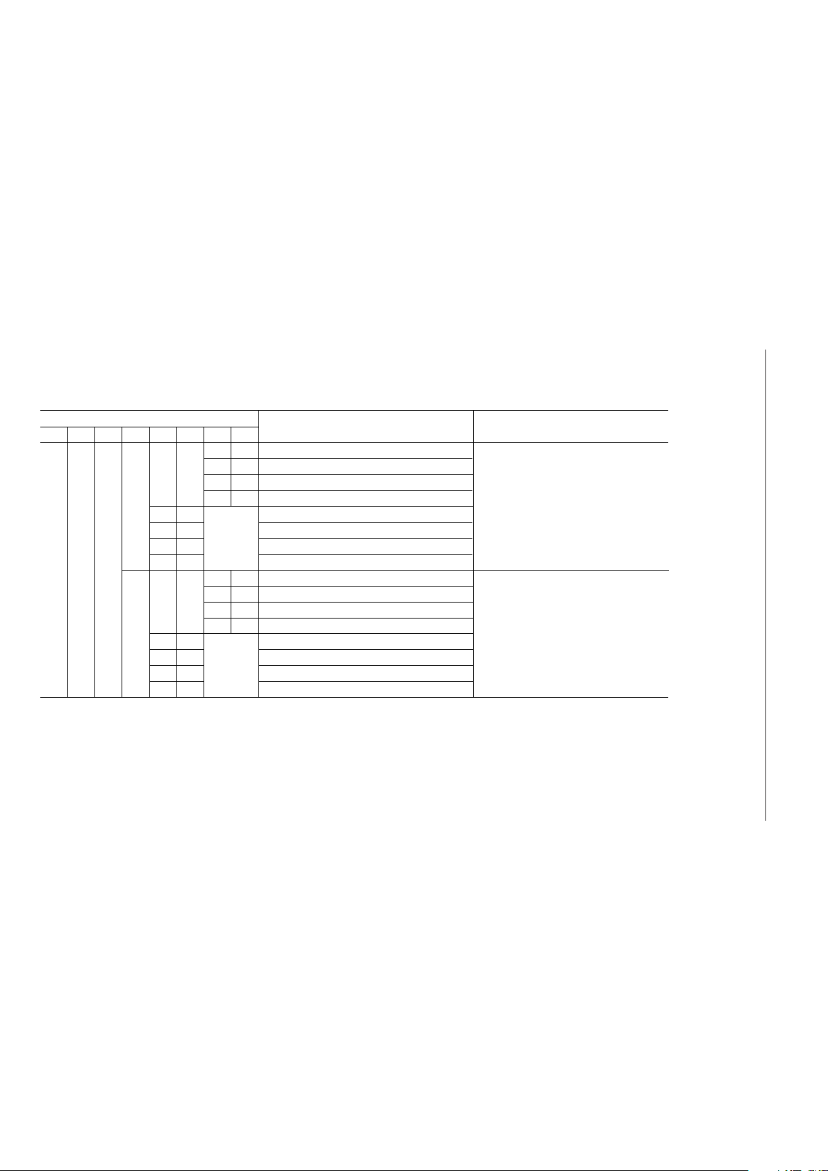
Gain control (transmit hold tone, PB tone, microphone input, handset input)
WRITE Mode
Address Data AD1 = 0, AD0 = 1
DB7
Typical transmit hold tone gain (–2 dB)
DB6 DB5 DB4 DB3 DB2 DB1 DB0
Control Data
Description for Control Remarks
0
00
01
10
11
01
00
——
—
—
—
—
0
–3 dB with respect to the typical gain
Transmit hold tone gain = VOL3
01
10
11
1
10
11
10
11
01
00
01
00
–6 dB with respect to the typical gain
–9 dB with respect to the typical gain
Typical transmit PB tone gain (+4 dB)
–3 dB with respect to the typical gain
–6 dB with respect to the typical gain
–9 dB with respect to the typical gain
Typical handfree input gain (+20 dB)
–6 dB with respect to the typical gain
–9 dB with respect to the typical gain
—
Typical handset input gain (+12 dB)
–3 dB with respect to the typical gain
–6 dB with respect to the typical gain
–9 dB with respect to the typical gain
Transmit PB tone gain = VOL4
Hold tone gain and PB tone
gain are set at a time.
At the initial setting, the typical gain is set.
Handfree input gain = VOL9
Handset input gain = VOL8
Handfree input gain and handset Input
gain are set at a time.
At the initial setting, the typical gain is set.
Page 29

¡ Semiconductor MSM7502
29/35
Gain control (receive PAD, speaker)
WRITE Mode
Address Data AD1 = 0, AD0 = 1
DB7
Typical speaker amp. gain (0 dB)
DB6 DB5 DB4 DB3 DB2 DB1 DB0
Control Data
Description for Control Remarks
1
00
01
10
11
10
1
-4 dB with respect to the typical gain
Speaker amp. gain = VOL5
1
1
1
00
—
—
—
—
—
10
0
0
0
1
0
00
01
0
0
0
0
00
01
10
11
01
11
00
01
10
11
10
0000
11
-8 dB with respect to the typical gain
-12 dB with respect to the typical gain
-16 dB with respect to the typical gain
-20 dB with respect to the typical gain
-24 dB with respect to the typical gain
-28 dB with respect to the typical gain
Typical additional speaker input path gain (0 dB)
-6 dB with respect to the typical gain
-12 dB with respect to the typical gain
-18 dB with respect to the typical gain
Speaker receive OFF(SW21 OFF)
Speaker receive ON (SW21 ON)
Typical receive PAD gain (0 dB)
-3 dB with respect to the typical gain
-6 dB with respect to the typical gain
-9 dB with respect to the typical gain
Typical incoming tone gain (0 dB)
-10 dB with respect to the typical gain
-20 dB with respect to the typical gain
Additional speaker gain = VOL6
Speaker amp. gain and additional
speaker gain are set at a time.
At the initial setting, SW21-OFF and the
typical gain are set.
Receive PAD = VOL10
Incoming tone gain = VOL11, VOL12
Receive PAD and incoming tone gain are
set at a time.
At the initial setting, the typical gain is set.
Page 30

¡ Semiconductor MSM7502
30/35
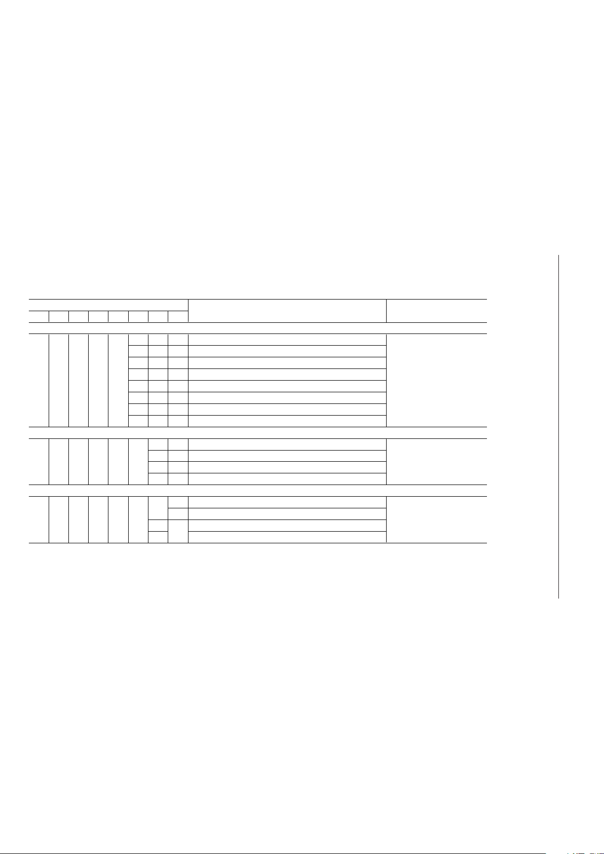
Key scanning signal output control
WRITE Mode
Address Data AD1 = 1, AD0 = 0
DB7
The data set on DB7 to DB0 are output on PO7 to PO0 respectively.
Output data is held until next data is written.
When the set data is set to "0", output data goes to "0", when set to "1", output pin becomes open.
At the initial setting, PO7 to PO0 are in open state.
DB6 DB5 DB4 DB3 DB2 DB1 DB0
Controlo Data
Description for Control
Output Data
Key scanning data read out
Read Mode
Address Data AD1 = 1, AD0 = 0
DB7
Data input onto PI7 to PI0 are output onto DB7 to DB0.
DB6 DB5 DB4 DB3 DB2 DB1 DB0
Contorol Data Description for Control
PI7 PI6 PI5 PI4 PI3 PI2 PI1 PI0
Key scanning interrupt reset
WRITE Mode
Address Data AD1 = 1, AD0 = 1
DB7
INTT output is reset (Output = 1)
DB6 DB5 DB4 DB3 DB2 DB1 DB0
Control Data
Description for Control
01
000000 Valid during write mode only
Remarks
Page 31
¡ Semiconductor MSM7502
31/35
Special functions
WRITE Mode
Address Data AD1 = 1, AD0 = 1
DB7
VLCD pin output voltage
: 0.0 V
DB6 DB5 DB4 DB3 DB2 DB1 DB0
Contorol Data
Description for Control Remarks
LCD Deflection Angle Control Voltage Output
000
001
010
011
100
101
110
111
01000
: 0.30 V
: 0.55 V
: 0.85 V
: 1.1 V
: 1.3 V
: 1.5 V
: 1.7 V
At the initial setting stage,
set to 0 V.
Power Down Mode Control
Whole system power down mode00
01
10
11
Whole system power ON mode
CODEC power down mode
CODEC power ON mode
100000
At the initial setting stage, set to
whole system power down mode.
CODEC power ON/OFF control is
valid in the whole system power
ON mode.
CODEC Control
CODEC operates in m-law0
1
0
1
CODEC operates in A-law
PCMIN and PCMOUT are normally connected
PCMOUT is connected to PCMIN
110000
At the initial setting stage, set to
m-law, and PCMIN and PCMOUT
are normally connected.
The componding law and the
connection control are set at a
time.
*2: Even during the whole system power down mode, following functions are available, if XSYNC is input. :
Key scanning data I/O, sounder outputs (SA0, SA1), WDT, INTT, and general latch output (LA, LB)
—
—
Page 32
¡ Semiconductor MSM7502
32/35
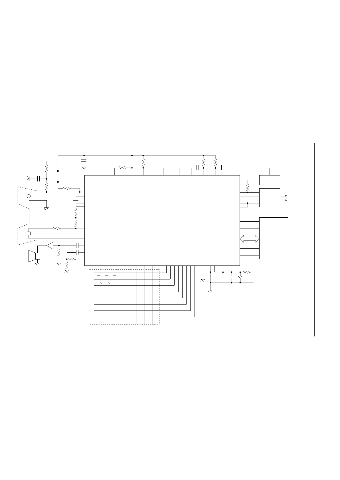
APPLICATION CIRCUIT
Line
Line
Interface
Controller
Hold Tone
Generator
*1*2Inserting a capacitor (1 mF to 22 mF)
between SGT and AG will improve
the transmit path noise
characteristic.
Insert a resistor if necessary.
*1
*2
100 kW
Speaker
Handset
SGT
TPAI
CAO
R1I
RPO
RMI
RMO0
RMO1
SPO
SPI
SAO
100 kW
0.1
m
F
100 kW
0.1 mF
+5 V
+5 V
0 V
0.1
m
F to 1 mF
0.1
m
F
10
m
F
+
+5 V
LML
PCMOUT
PCMIN
BCLOCK
XSYNC
WRN
RDN
CEN
RESETN
AD0
AD1
INTT
TIMEN
RSYNC
DB0 to DB7
MPAI TPAO TPBI MPBI MPBOMPAO TO CAI MLDYI
PO0 PO1 PO2 PO3 PO4 PO5 PO6 PO7
SW Matrix
PI0
PI1
PI2
PI3
PI4
PI5
PI6
PI7
SGCAGDGVAVD
0-20 W
Page 33
¡ Semiconductor MSM7502
33/35
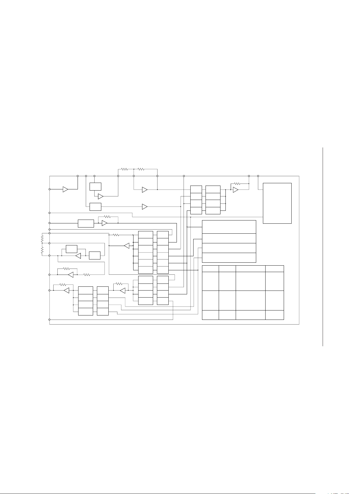
MSM7502 Speech Path Level Setting
TPAO
MLDYI
TO CAITPBI
MPAO
MPAI
+
–
20 dB
AIN
AOUT
CODEC
RMO0
R1I
CAO
TPAI
SPO
RMO1
MPBI MPBO
R2I
0 dB
SPI
SW5
SW5
SW1
SW2
SW7
SW16
5.7 dB
0 dB
VOL 3
VOL 4
RPO
RMI
SW21
SW20
SW11
SW15
VOL 5
VOL 12
VOL 11
–
22 dB
SW18
–
6.8 dB
SW10VOL 6
SW8
–
3 dB
SW6
0 dB
SW3VOL 1
SW4VOL 2
SW13VOL 7
SW17
–
8.7 dB
SW14
0 dB
SW9
0 dB
–
20 dB to +25 dB
Variable Range
Step Width
Typical Level
VOL No.
–14 dB to 0 dB
–21 dB to –3 dB
–11 dB to –2 dB
–5 dB to +4 dB
–28 dB to 0 dB
–6 dB
–9 dB
–2 dB
+4 dB
0 dB
0 dB
0 dB
+12 dB
+20 dB
0 dB
0 dB
0 dB
VOL 6
VOL 7
VOL 8
VOL 9
VOL 10
VOL 11
VOL 12
VOL 1
VOL 2
VOL 3
VOL 4
VOL 5
–18 dB to 0 dB
90 mV to 180 mV
+3 dB to +12 dB
+11 dB to +20 dB
–9 dB to 0 dB
–20 dB to 0 dB
–20 dB to 0 dB
2 dB
3 dB
3 dB
3 dB
4 dB
6 dB
30 mV
3 dB
3,6 dB
3 dB
10 dB
10 dB
VOL 10
VOL 9
VOL 8
–
+
+
–
–
–
CODEC I/O Level
Overload Point: 1.2 V
op
0 dBmO : 0.6007 Vrms
(–4.4 dBV)
PB GEN.
Per Wave
0.24 V
PP
(–21.4 dBV Equivalent)
R-Tone GEN.
90 mV
PP
Pulse (–27.8 dBV Equivalent)
F-Tone GEN.
0.16 V
PP
Pulse (–22.8 dBV Equivalent)
S-Tone GEN.
0.22 V
PP
Pulse (–20.0 dBV Equivalent)
–
–
–
Page 34

¡ Semiconductor MSM7502
RECOMMENDATIONS FOR ACTUAL DESIGN
• To assure proper electrical characteristics, use bypass capacitors with excellent high frequency
characteristics for the power supply and keep them as close as possible to the VA and AG pins.
• Connect the AG pin and the DG pin each other as close as possible. Connect to the system
ground with low impedance.
• Connect the VA pin and the VD pin as close together as possible and route them to the analog
5 V power supply.
• Mount the device directly on the board when mounted on PCBs. Do not use IC sockets. If an
IC socket is unavoidable, use the short lead type socket.
• When mounted on a frame, use electro-magnetic shielding, if any electro-magnetic wave
source such as power supply transformers surround the device.
• Keep the voltage on the VDD pin not lower than –0.3 V even instantaneously to avoid latch-up
phenomenon when turning the power on.
• Use a low noise (particularly, low level type of high frequency spike noise or pulse noise) power
supply to avoid erroneous operation and the degradation of the characteristics of these devices.
• Connect analog input pins and digital input pins that are not used to the SG pin and to GND,
respectively.
• When the data is written differently from the data defined in the section, Control Data
Description in FUNCTIONAL DESCRIPTION, normal device operation is not guaranteed.
34/35
Page 35

¡ Semiconductor MSM7502
PACKAGE DIMENSIONS
(Unit : mm)
QFP80-P-1420-0.80-BK
Mirror finish
Package material
Lead frame material
Pin treatment
Solder plate thickness
Package weight (g)
Epoxy resin
42 alloy
Solder plating
5 mm or more
1.27 TYP.
Notes for Mounting the Surface Mount Type Package
The SOP, QFP, TSOP, SOJ, QFJ (PLCC), SHP and BGA are surface mount type packages, which
are very susceptible to heat in reflow mounting and humidity absorbed in storage.
Therefore, before you perform reflow mounting, contact Oki’s responsible sales person for the
product name, package name, pin number, package code and desired mounting conditions
(reflow method, temperature and times).
35/35
 Loading...