

Page 1

E2F0005-29-12
¡ Semiconductor
This version: Jan. 1999
Previous version: Mar. 1998
MSM7630¡ Semiconductor
MSM7630
Universal Speech Processor
GENERAL DESCRIPTION
The MSM7630 is a speech processor LSI device with internal D/A converter. It is optimized for
speech output applications such as text-to-speech conversion.
FEATURES
• Parallel and serial interfaces
• Single 3.3V power supply
• 5V interface available
• Internal 16-bit x 16-bit to 32-bit multiplier (2-clock data throughput)
• 26 VAX MIPS performance at 40 MHz operation (when using ordinary ROM/SRAM)
• Package: 100-pin plastic QFP (QFP100-P-1420-0.65-BK)(Product name: MSM7630GS-BK)
1/95
Page 2
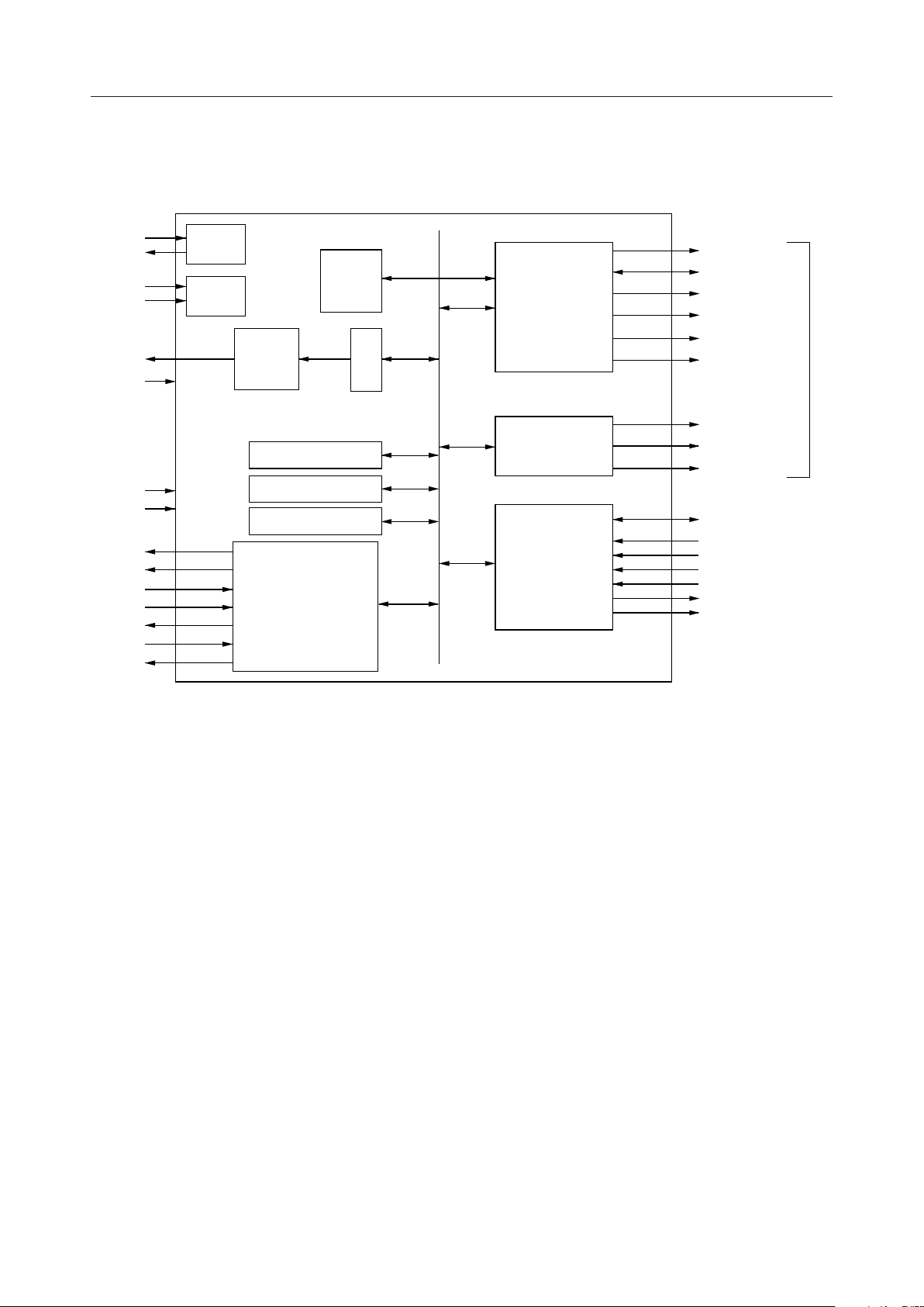
BLOCK DIAGRAM
MSM7630¡ Semiconductor
CLK
MCLKA
TSTM
EXINT
DAO1
SG
RST
STBY
SCLK
TXD
RXD
DSR
DTR
CTS
RTS
PLL
TST
DAC
TMR
TMR
TMR
SIO
MPY
REG
CPU
DRAMC
PIO
A23-0
D31-16
WR0,1
RD
ROM
SRAM
Local Bus
RAS
CAS0,1
WE
PD7-0
PSTB
PACK
PCS
PIOA
POBF
PIBF
2/95
Page 3
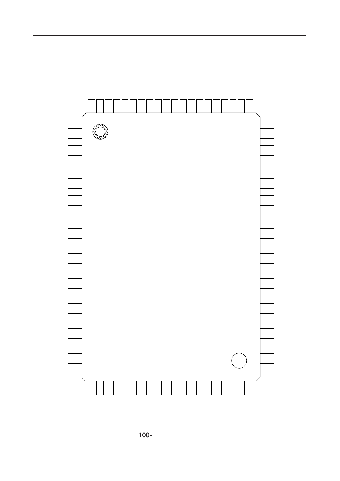
PIN CONFIGURATION (TOP VIEW)
DAO1
TEST0SGVDDVDDGND
99989796959493929190898887868584838281
100
GNDXOCLK
CLKA
UPORT
TSTM2
TSTM1
VDDEXTINT
A23
A22
A21
A20
MSM7630¡ Semiconductor
A19
GND
GND
RST
RD
STBY
WR1
WR0
AS
ROM
V
DD
SRAM
D31
D30
D29
D28
D27
GND
D26
D25
D24
D23
D22
D21
V
DD
D20
D19
D18
D17
D16
PD7
10
11
12
13
14
15
16
17
18
19
20
21
22
23
24
25
26
27
28
29
30
80
79
78
77
76
75
74
73
72
71
70
69
68
67
66
65
64
63
62
61
60
59
58
57
56
55
54
53
52
51
A18
GND
A17
A16
A15
A14
A13
A12
V
DD
A11
A10
A9
A8
A7
A6
A5
GND
A4
A3
A2
A1
A0
CAS1
CAS0
V
DD
WE
SCLK
RXD
RAS
TXD
1
2
3
4
5
6
7
8
9
31323334353637383940414243444546474849
PD6
GND
PD5
PD4
PD3
PD2
PD1
PD0
PIOA
V
PCS
PACK
PIBF
PSTB
POBF
DSR
RTS
GND
CTS
DD
100-Pin Plastic QFP
50
DTR
3/95
Page 4

PIN DESCRIPTIONS
MSM7630¡ Semiconductor
Symbol
D31-16
A23-0
ROM
SRAM
RD
WR0,1
WE
AS
TXD
RXD
DTR
DSR
RTS
CTS
SCLK
PD7-0
PACK
PSTB
PCS
PIOA
POBF
PIBF
UPORT
TEST0
DAO1
SG
CLK
XO
CLKA
RST
STBY
EXTINT
TSTM2,1
Type
I/O
O
O
O
O
O
ORAS
OCAS0,1
O
O
O
I
O
I
O
I
O
I/O
I
I
I
I
3-state
3-state
O
I
O
I
I
O
O
I
I
I
I
Description
16-bit data bus. 8-bit devices are accessed through D31-24.
24-bit address bus. DRAM addresses are output from A13-0.
ROM select signal. ROM indicates that ROM space is assigned to the specified address.
It is used as a chip select signal.
SRAM select signal. SRAM indicates that SRAM space is assigned to the specified address.
It is used as a chip select signal.
Read signal. RD is active during both 8-bit and 16-bit reads.
Write signals. WR0 corresponds to writes from D31-24, and WR1 corresponds to
writes from D23-16.
Row address strobe. RAS is active during both 8-bit and 16-bit reads.
Column address strobe. CAS0 corresponds to accesses from D31-24, and CAS1
corresponds to accesses from D23-16.
Write enable. WE is active during writes to DRAM space as the DRAM write signal.
Address strobe.
Serial data output.
Serial data input.
Control signal indicating SIO can transmit and receive.
Input signal indicating that modem is in operable state.
SIO transmit request signal.
Input signal indicating that modem can transmit.
Synchronous transfer clock output.
Parallel port data input/output.
Parallel port read signal. Set high for Centronics interface.
Parallel port write signal. Strobe signal for Centronics interface.
Parallel port chip select signal.
Parallel port address signal. Selects data or status during an access.
Output port buffer full. Indicates that data has been set in the output buffer.
Input port buffer full. Indicates that there is data in the input buffer.
Busy output signal for Centronics interface.
General flag output signal.
Connects with SG.
D/A converter output.
Signal ground. Connects with TEST0.
Clock input signal.
Clock signal. Inverse of CLK.
Internal clock signal.
Reset input.
Standby signal. STBY suspends operation and places the MSM7630 in a standby state.
External interrupt signal.
Test mode select input signal.
4/95
Page 5
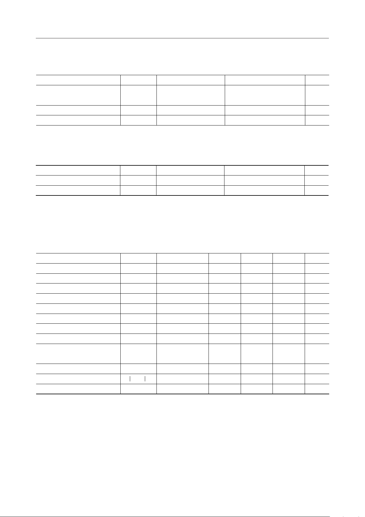
ABSOLUTE MAXIMUM RATINGS
MSM7630¡ Semiconductor
Parameter Symbol Condition
Power Supply Voltage V
Input Voltage V
Storage Temperature T
DD
IN
STG
Ta = 25°C
(excluding TEST0)
Ta = 25°C
—
RECOMMENDED OPERATING CONDITIONS
Parameter Symbol Conditon
Power Supply Voltage V
Operating Temperature T
DD
op
—
—
ELECTRICAL CHARACTERISTICS
DC Characteristics
Parameter Symbol Condition
"H" Input Voltage V
"L" Input Voltage V
"H" Input Voltage V
"L" Input Voltage V
"H" Output Voltage V
"L" Output Voltage V
Input Leakage Current I
Output Leakage Current I
Dynamic Supply Current I
Static Supply Current I
D/A Output Relative Accuracy V
D/A Output Impedance R
IH
IL
IH
IL
OH
OL
LI
LO
DO
DS
DAE
DA
Excluding CLK
Excluding CLK
CLK
CLK
= –4 mA
I
OH
I
= 4 mA
OL
0 £ V
0 £ V
f
V
DD
OPE
£ V
IN
DD
£ V
OUT
= 3.6 V,
= 20 MHz
—
No load
—
DD
Rating
–0.3 to +4.5
–0.3 to +5.5 V
–55 to +125 °C
Range
3.0 to 3.6
–40 to +85 °C
= 3.0 to 3.6 V, Ta = –40 to +85°C)
(V
DD
Min. Typ. Max.
2.2
—
0.8 ¥ V
—
2.4
—
–10
–10
—
—
—
12
DD
—
—
—
—
—
—
—
—
—
—
—
20
0.2 ¥ V
Unit
V
Unit
V
Unit
—
V
0.8 V
—V
DD
V
—V
0.4 V
+10 mA
+10 mA
120 mA
1.5 mA
10 mV
28 kW
5/95
Page 6

AC Characteristics
MSM7630¡ Semiconductor
Parameter Symbol Condition
Source Oscillation Period t
Input Clock Low-Level
t
W_CLKL
Minimum Width
Input Clock High-Level
t
W_CLKH
Minimum Width
Operating Period t
CLKA Delay Time t
XO Delay Time t
Required RST Time t
W_RST
A Delay Time t
D Setup Time t
D Hold Time t
D Delay Time t
RD Delay Time t
WR Delay Time t
UPORT Delay Time t
EXINT Setup Time t
UPORT
S_EXINT
OSC
CYC
CLK
XO
A
S_D
H_D
D
RD
WR
—
—
—
—
—
—
—
—
—
—
—
—
Falling
Rising
—
—
(VDD = 3.0 to 3.6 V, T
= –40 to +85°C)
OPE
Min. Typ. Max.
25
13
8
25
—
—
1024
—
2
6
—
—
—
—
—
2
—
—
—
—
—
—
—
—
—
—
—
—
—
—
—
—
50
—ns
—ns
50 ns
12 ns
7ns
—t
22 ns
—ns
—ns
25 ns
20 ns
22 ns
22 + 0.5 t
20 ns
—ns
CYC
Unit
ns
CYC
ns
6/95
Page 7

ROM, SRAM Access
Parameter Symbol Condition
RD Pulse Width t
WR Pulse Width t
A to RD Time t
A to WR Time t
WR to SRAM Time t
ROM Delay Time t
SRAM Delay Time t
ROM Pulse Width t
SRAM Pulse Width t
WR to D Time t
W_RD
W_WR
W_ARD
W_AWR
W_WRSRAM
ROM
SRAM
W_ROM
W_SRAM
W_WRD
ROM, SRAM
3t to 12t Access
SRAM
3t to 12t Access
ROM, SRAM
3t, 4t Access
ROM, SRAM
5t to 12t Access
SRAM
3t to 12t Access
SRAM
3t to 12t Access
—
—
ROM
3t to 12t Access
SRAM
3t to 12t Access
SRAM
3t Access
SRAM
4t to 12t Access
(V
= 3.0 to 3.6 V, T
DD
= –40 to +85°C)
OPE
Min. Typ. Max.
2
1.5
—
—
—
—
—
—
3
3
—
—
—
—
—
—
—
—
11 t
10.5 t
1
2
1
1
—t
—t
—t
—t
20 + 0.5 t
20 + 0.5 t
12 t
12 t
0
1
—t
—t
MSM7630¡ Semiconductor
CYC
CYC
Unit
CYC
CYC
CYC
CYC
CYC
CYC
ns
ns
CYC
CYC
CYC
CYC
7/95
Page 8
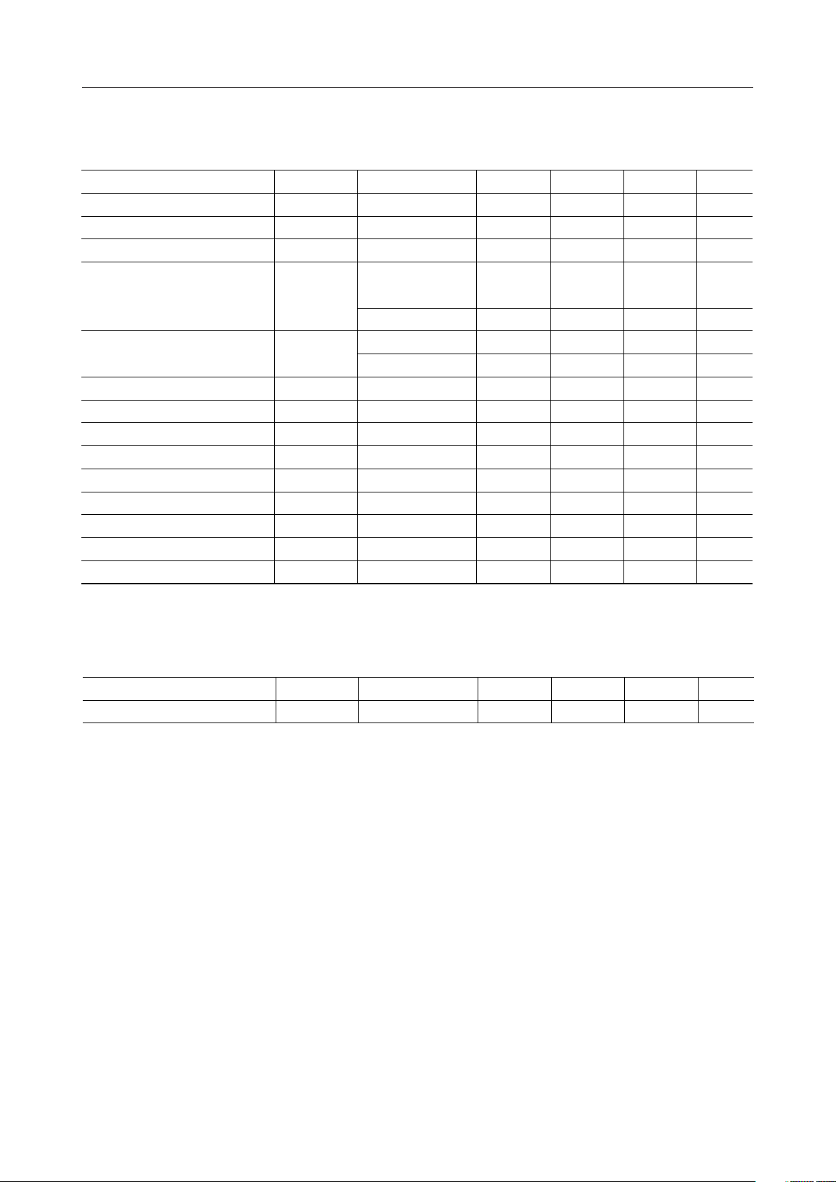
DRAM Access
Parameter Symbol Condition
RAS Delay Time t
RAS Pulse Width t
A to RAS Time t
CAS Delay Time t
CAS Pulse Width t
A to CAS Time t
RAS to CAS Time t
WE to CAS Time t
WE Delay Time t
WE Pulse Width t
A to WE Time t
Required Precharge Time t
CAS to RAS Time t
CAS to D Time t
RAS
W_RAS
W_ARAS
CAS
W_CAS
W_ACAS
W_RASCAS
W_WECAS
WE
W_WE
W_AWE
W_PREC
W_CASRAS
W_EDO
—
—
—
2nt access falling
edge
Normal
Normal
Refresh
—
—
—
—
—
—
—
—
Hyper Mode
(V
= 3.0 to 3.6 V, T
DD
= –40 to +85°C)
OPE
Min. Typ. Max.
—
3
1
—
—
1.5
4
0.5
1.5
1.5
—
3
—
1
—
—
—
—
—
—
—
—
—
—
—
—
—
—
—
—
18 ns
Note 1 t
—t
18 + 0.5 t
18 ns
2t
5t
1ns
2t
2t
20 ns
Note 1 t
1
—t
Note 2 t
1
—t
1t
MSM7630¡ Semiconductor
CYC
Unit
CYC
CYC
ns
CYC
CYC
CYC
CYC
CYC
CYC
CYC
CYC
CYC
General Device Access
Parameter Symbol Condition
AS Delay Time t
AS
—
= 3.0 to 3.6 V, T
(V
DD
= –40 to +85°C)
OPE
Min. Typ. Max.
—
—
18 ns
Unit
8/95
Page 9

When DS bit = 0
MSM7630¡ Semiconductor
Parameter Symbol Condition
AS Pulse Width t
A to AS Time t
RD Pulse Width t
A to RD Time t
WR Pulse Width t
A to WR Time t
D to WR Time t
W_AS
W_AAS
W_RD
W_ARD
W_WR
W_AWR
W_DWR
4t to 7t Access
(X bit = 0)
8t to 14t Access
(X bit = 1)
4t to 7t Access
(X bit = 0)
8t to 14t Access
(X bit = 1)
4t to 7t Access
(X bit = 0)
8t to 14t Access
(X bit = 1)
4t to 7t Access
(X bit = 0)
8t to 14t Access
(X bit = 1)
4t to 7t Access
(X bit = 0)
8t to 14t Access
(X bit = 1)
4t to 7t Access
(X bit = 0)
8t to 14t Access
(X bit = 1)
4t to 7t Access
(X bit = 0)
8t to 14t Access
(X bit = 1)
= 3.0 to 3.6 V, T
(V
DD
= –40 to +85°C)
OPE
Min. Typ. Max.
2
6
—
—
2
6
—
—
2
6
—
—
—
—
—
—
—
—
—
—
5t
12 t
1
1
—t
—t
5t
12 t
1
1
—t
—t
5t
12 t
1
1
0
0
—t
—t
—t
—t
Unit
CYC
CYC
CYC
CYC
CYC
CYC
CYC
CYC
CYC
CYC
CYC
CYC
CYC
CYC
9/95
Page 10

When DS bit = 1
Parameter Symbol Condition
AS Pulse Width
Note 3
A to AS Time t
RD Pulse Width t
A to RD Time t
WR Pulse Width t
A to WR Time t
D to WR Time t
t
W_AS
W_AAS
W_RD
W_ARD
W_WR
W_AWR
W_DWR
4t to 7t Access
(X bit = 0)
8t to 14t Access
(X bit = 1)
4t to 7t Access
(X bit = 0)
8t to 14t Access
(X bit = 1)
4t to 7t Access
(X bit = 0)
8t to 14t Access
(X bit = 1)
4t to 7t Access
(X bit = 0)
8t to 14t Access
(X bit = 1)
4t to 7t Access
(X bit = 0)
8t to 14t Access
(X bit = 1)
4t to 7t Access
(X bit = 0)
8t to 14t Access
(X bit = 1)
4t to 7t Access
(X bit = 0)
8t to 14t Access
(X bit = 1)
(V
= 3.0 to 3.6 V, T
DD
= –40 to +85°C)
OPE
Min. Typ. Max.
2
6
—
—
2
6
—
—
2
6
—
—
—
—
—
—
—
—
—
—
5t
12 t
1
1
—t
—t
5t
12 t
1
1
—t
—t
5t
12 t
2
3
1
2
—t
—t
—t
—t
MSM7630¡ Semiconductor
Unit
CYC
CYC
CYC
CYC
CYC
CYC
CYC
CYC
CYC
CYC
CYC
CYC
CYC
CYC
10/95
Page 11
Serial Interface
MSM7630¡ Semiconductor
Parameter Symbol Condition
RTS Delay Time t
Required RXD Time t
RXD Setup Time t
RXD Hold Time t
CTS Setup Time t
CTS Hold Time t
TXD Delay Time t
TXD Pulse Width t
DTR Delay Time t
SCLK Delay Time t
SCLK Pulse Width t
Parallel Interface
Parameter Symbol Condition
PACK to PD Delay Time t
PACK to PD Hi Z Delay Time t
PCS Setup Time for PSTB/PACK
PCS Hold Time for PSTB/PACK t
PIOA Setup Time for PSTB/PACK
PIOA Hold Time for PSTB/PACK t
Required PACK Time t
Required PSTB Time t
PD Setup Time for PSTB t
PD Hold Time for PSTB t
RTS
W_RXD
S_RXD
H_RXD
S_CTS
H_CTS
TXD
W_TXD
DTR
SCLK
W_SCLK
PACK
PRDZ
t
S_PCS
H_PCS
t
S_PIOA
H_PIOA
W_PACK
W_PSTB
S_PD
H_PD
—
—
—
—
—
—
—
—
—
—
—
—
—
—
—
—
—
—
—
—
—
= 3.0 to 3.6 V, T
(V
DD
Min. Typ. Max.
—
1/bps
0.5/bps
0.5/bps
0
0
—
1/bps
—
—
1/bps
(V
DD
—
—
—
—
—
—
—
—
—
—
—
= 3.0 to 3.6 V, T
Min. Typ. Max.
—
—
0
0
0
3
30 + t
30 + 2 t
–t
CYC
8
CYC
CYC
—
—
—
—
—
—
—
—
—
—
= –40 to +85°C)
OPE
Unit
20 ns
—s
—
—
—
—
s
s
ns
ns
20 ns
—s
20 ns
20 ns
—s
= –40 to +85°C)
OPE
Unit
22 ns
22 ns
—ns
—ns
—ns
—ns
—ns
—ns
—ns
—ns
Note 1 According to DRAM configuration
Note 2 By the DRAM access timing
Note 3 In the case of writing, increased by 1 clock when X bit = 0 and by 2 clocks when X bit
= 1.
Note 4 Flash memory access timing is the same with the SRAM timing.
11/95
Page 12
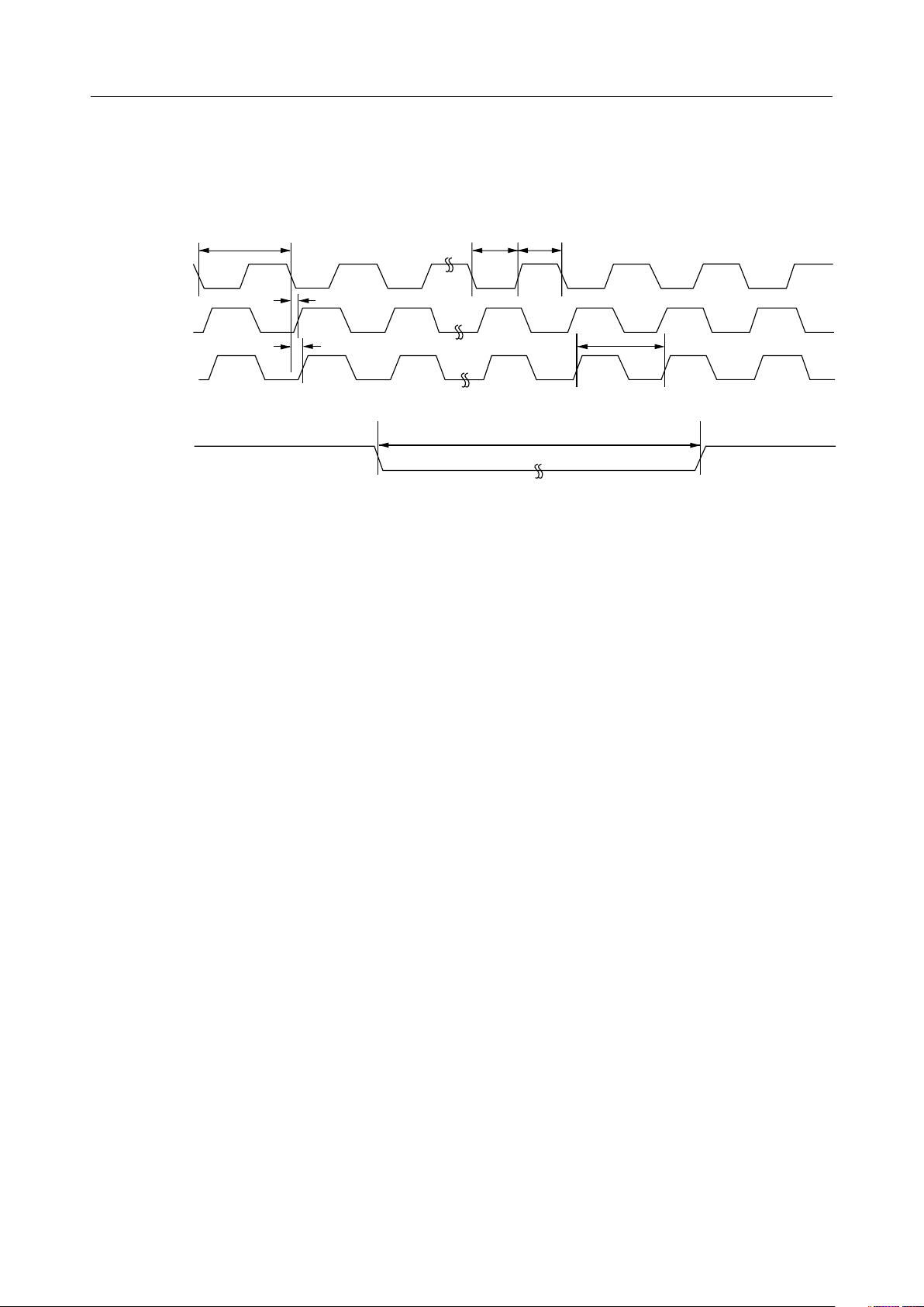
TIMING DIAGRAM
Clock And Reset
t
OSC
CLK
XO
CLKA
RST
t
XO
t
CLKA
t
W_CLKLtW_CLKH
t
W_RST
t
MSM7630¡ Semiconductor
CYC
12/95
Page 13
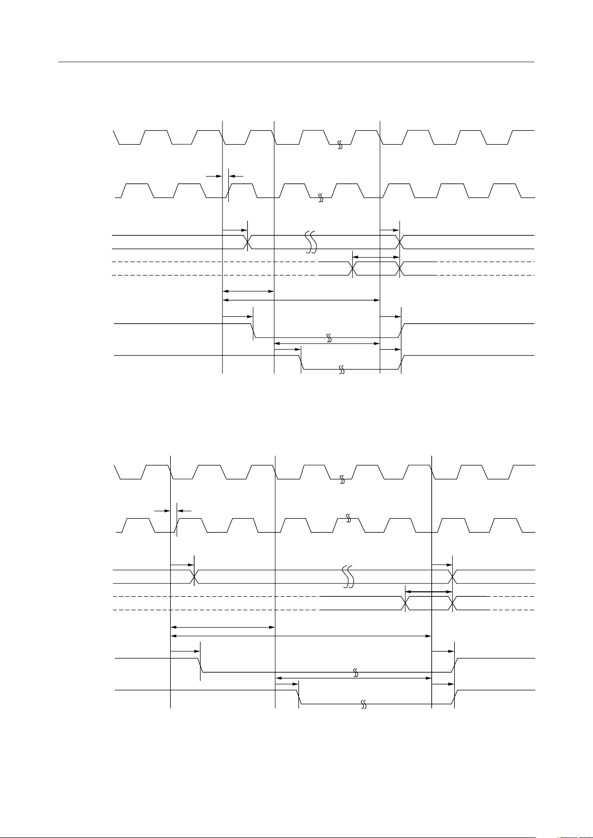
ROM Read
CLK
CLKA
t
CLKA
MSM7630¡ Semiconductor
ROM
RD
CLK
CLKA
t
A
A
t
S_D
D
t
t
CLKA
t
ROM
W_ARD
t
RD
tt
3
t/4
tt
tt
t Access
tt
t
W_ROM
t
W_RD
t
A
t
H_D
t
ROM
t
RD
ROM
RD
t
A
A
t
S_D
D
t
t
ROM
W_ARD
5
tt
t/6
tt
t
tt
t/8
tt
RD
tt
t/10
tt
t
W_ROM
tt
t/12
tt
tt
t Access
tt
t
W_RD
t
A
t
H_D
t
ROM
t
RD
13/95
Page 14
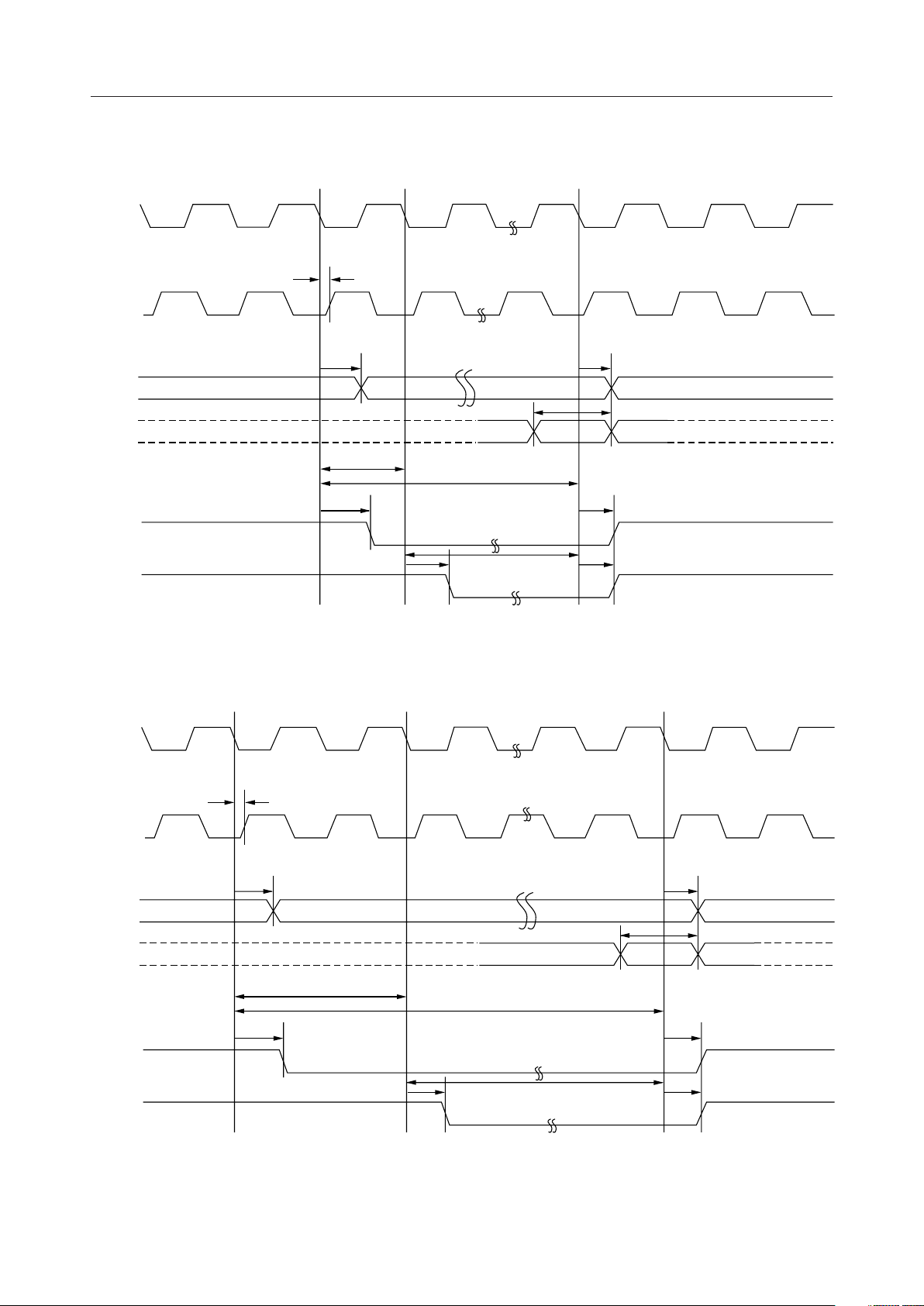
SRAM Read
CLK
CLKA
t
CLKA
MSM7630¡ Semiconductor
SRAM
RD
CLK
CLKA
t
A
t
A
A
t
S_D
t
H_D
D
t
t
CLKA
t
SRAM
W_ARD
t
W_SRAM
t
SRAM
t
RD
tt
tt
3
t/4
t Access
tt
tt
t
W_RD
t
RD
SRAM
RD
t
A
t
A
A
t
S_D
t
H_D
D
t
t
SRAM
W_ARD
5
tt
t/6
tt
t
RD
tt
t/8
tt
t
W_SRAM
tt
t/10
tt
tt
t/12
tt
t
W_RD
tt
t Access
tt
t
SRAM
t
RD
14/95
Page 15
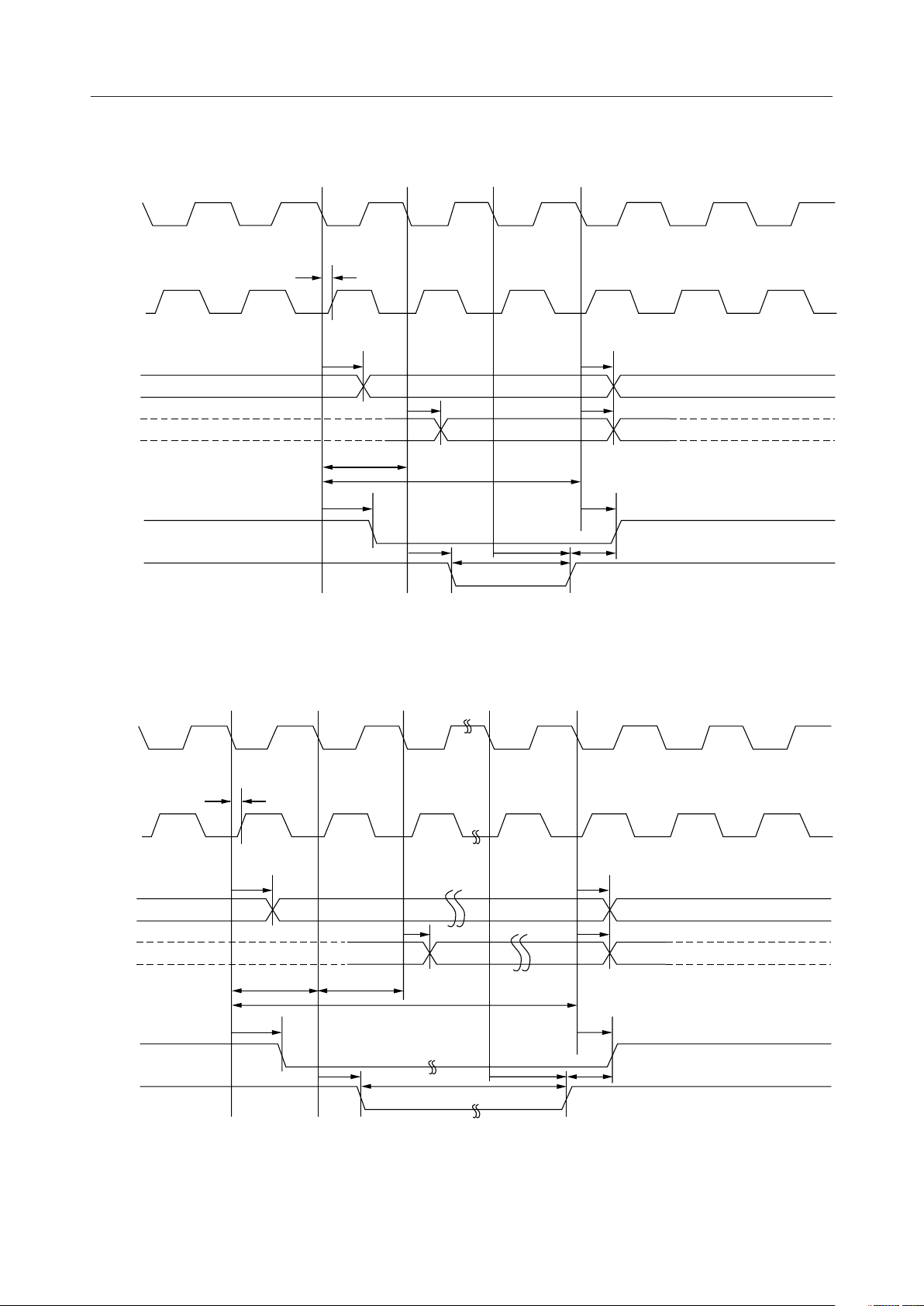
SRAM Write
CLK
CLKA
t
CLKA
MSM7630¡ Semiconductor
SRAM
WR
CLK
CLKA
t
A
t
A
A
t
D
t
D
D
t
t
CLKA
t
SRAM
W_AWR
t
WR
t
W_SRAM
t
tt
3
t Access
tt
WR
t
W_WR
t
SRAM
t
W_WRSRAM
SRAM
WR
t
A
t
A
A
t
D
t
D
D
t
SRAM
t
W_AWR
t
WR
t
W_WRD
tt
4
t/5
tt
tt
t/6
tt
tt
t/8
tt
t
W_SRAM
t
W_WR
tt
t/10
tt
t
WR
tt
t/12
tt
tt
t Access
tt
t
SRAM
t
W_WRSRAM
15/95
Page 16
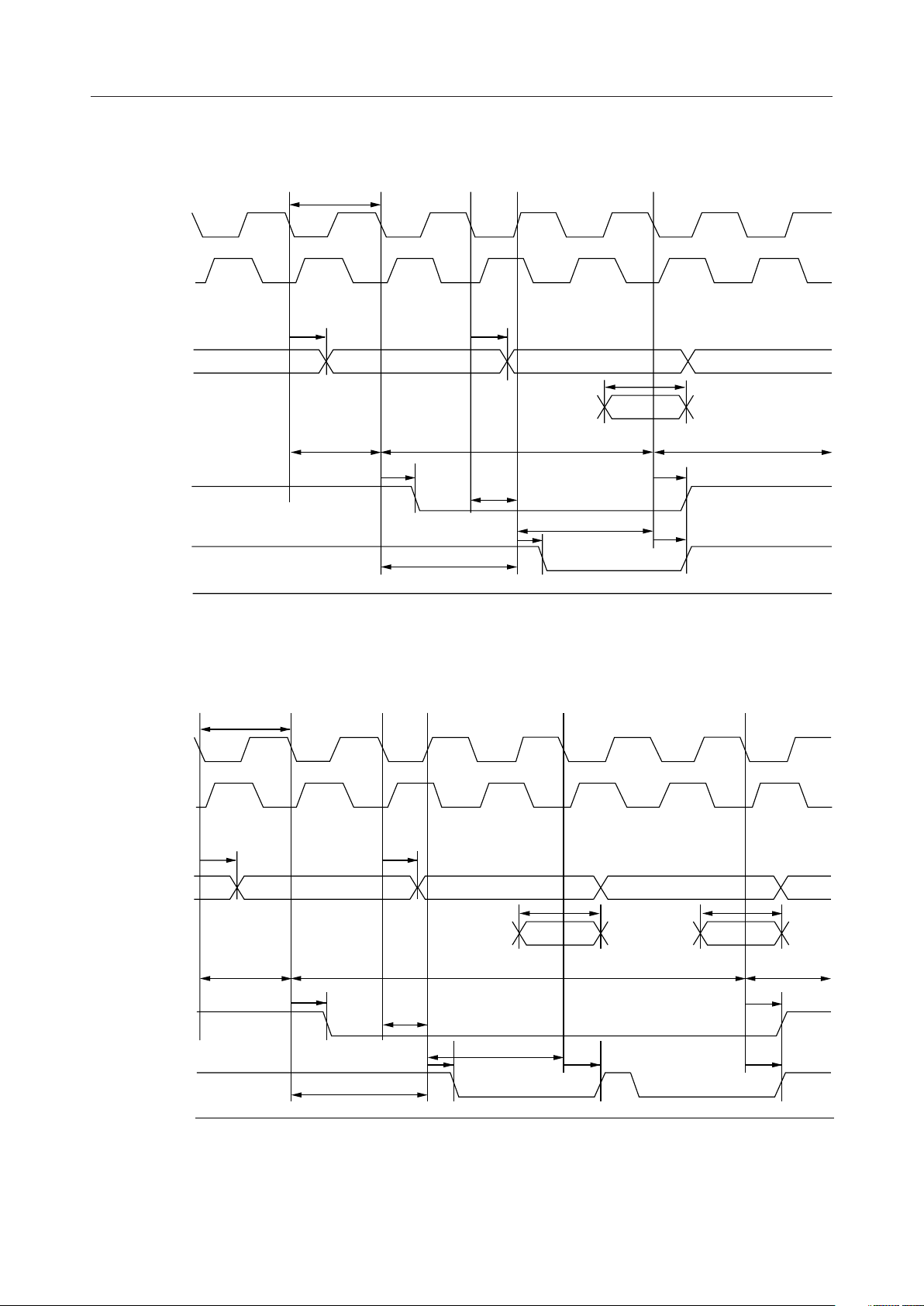
DRAM Read
CLK
CLKA
t
OSC
MSM7630¡ Semiconductor
RAS
CAS
WE
CLK
t
A
A
row address column address
t
A
t
S_D
t
H_D
D
t
OSC
t
W_ARAS
t
RAS
t
W_RASCAS
tt
2n
t Access (Fast Page Mode)
tt
t
CAS
t
W_RAS
t
W_ACAS
t
W_CAS
t
RAS
t
CAS
t
W_PREC
CLKA
RAS
CAS
WE
t
A
A
row address column address
t
A
column address
t
S_D
t
H_D
t
S_D
t
H_D
D
t
W_ARAS
t
RAS
t
W_ACAS
t
CAS
t
W_RASCAS
tt
2n
t Access (Fast Page Mode)
tt
t
t
W_CAS
W_RAS
t
CAS
t
t
RAS
W_PREC
t
CAS
16/95
Page 17
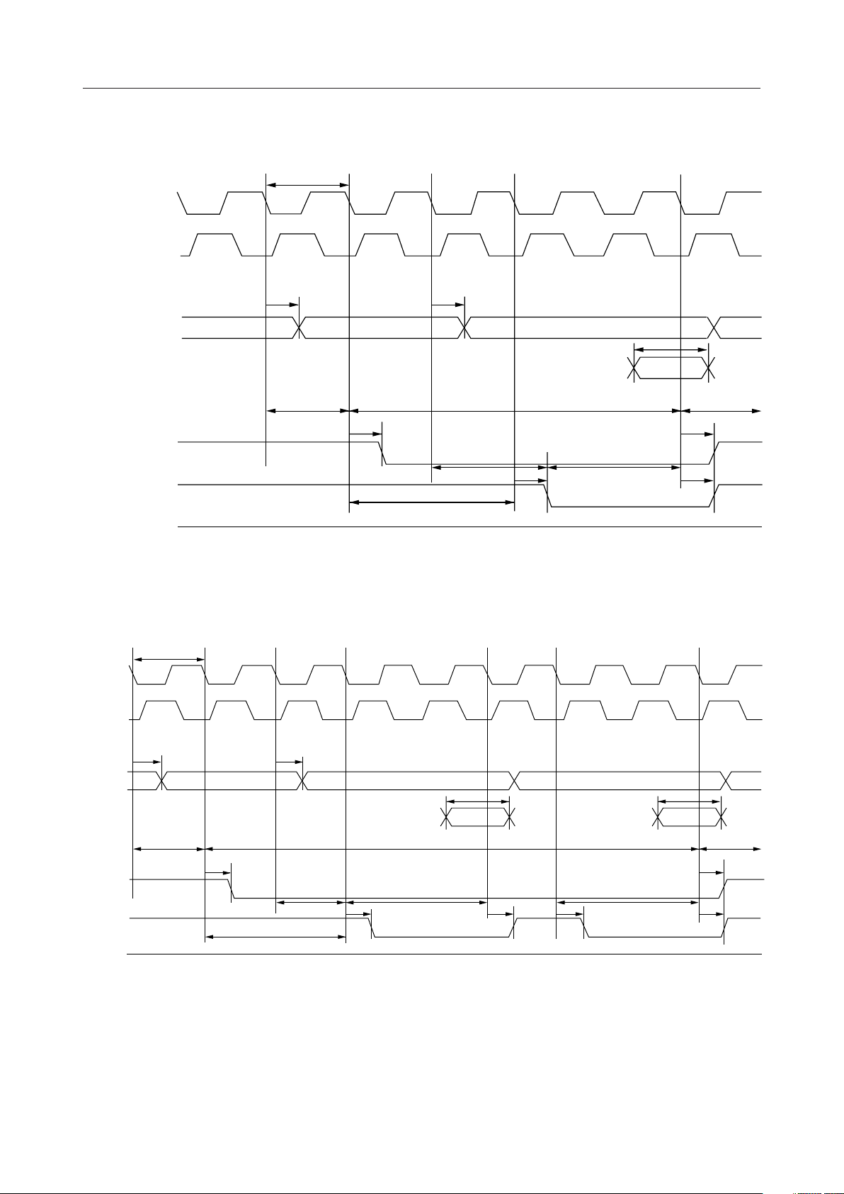
CLK
CLKA
t
OSC
MSM7630¡ Semiconductor
CLK
RAS
CAS
WE
t
A
A
row address
t
A
column address
t
S_D
t
H_D
D
t
OSC
t
W_ARAS
t
RAS
t
W_RASCAS
tt
3n
t Access (Fast Page Mode)
tt
t
W_ACAS
t
CAS
t
W_RAS
t
W_CAS
t
W_PREC
t
RAS
t
CAS
CLKA
RAS
CAS
WE
t
A
A
D
t
W_ARAS
t
RAS
t
t
W_RASCAS
A
column addressrow address
t
S_D
t
W_RAS
t
W_ACAS
t
CAS
tt
3n
t Access (Fast Page Mode)
tt
t
W_CAS
t
t
CAS
H_D
column address
t
S_D
t
W_CAS
t
CAS
t
W_PREC
t
RAS
t
t
H_D
CAS
17/95
Page 18
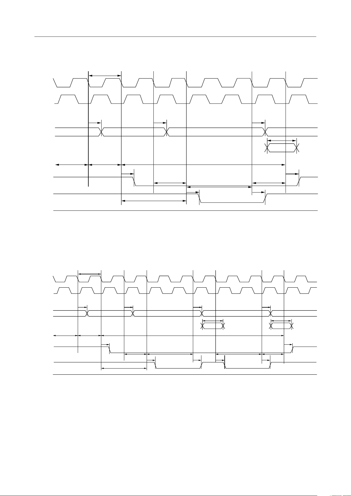
CLK
CLKA
t
MSM7630¡ Semiconductor
OSC
RAS
CAS
WE
CLK
t
A
A
row address
t
A
t
A
column address
t
S_D
t
H_D
D
t
OSC
t
W_ARAS
t
W_RAS
t
RAS
t
W_ACAS
t
t
W_RASCAS
tt
3n
t Access (Hyperpage Mode)
tt
CAS
t
W_CAS
t
W_EDO
t
CAS
t
RAS
t
W_PREC
CLKA
RAS
CAS
WE
t
A
A
D
t
W_PREC
t
W_ARAS
t
RAS
t
t
W_RASCAS
3n
A
t
A
column addressrow address
t
S_D
t
W_RAS
t
W_ACAS
t
CAS
tt
t Access (Hyperpage Mode)
tt
t
W_CAS
t
CAS
column address
t
H_D
t
W_CAS
t
CAS
t
t
S_D
t
A
W_EDO
t
CAS
t
RAS
t
H_D
18/95
Page 19
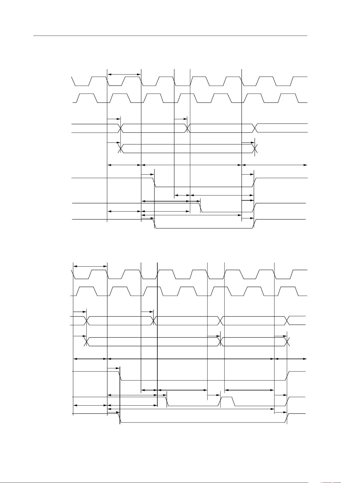
DRAM Write
CLK
CLKA
t
MSM7630¡ Semiconductor
OSC
RAS
CAS
WE
CLK
t
A
A
t
D
row address column address
t
A
t
D
D
t
OSC
t
W_ARAS
t
RAS
t
t
W_WECAS
WE
W_ACAS
t
W_RASCAS
t
W_AWE
t
tt
2n
t Access (Fast Page Mode)
tt
t
W_RAS
t
W_WE
t
CAS
t
W_CAS
t
RAS
t
WE
t
CAS
t
W_PREC
CLKA
RAS
CAS
WE
t
A
A
t
D
row address
t
A
column address column address
t
D
t
D
D
t
CAS
t
t
W_CAS
W_RAS
t
W_WE
t
CAS
t
W_CAS
t
CAS
t
WE
t
W_PREC
t
W_ARAS
t
W_AWE
t
RAS
t
W_RASCAS
t
W_ACAS
t
W_WECAS
t
WE
tt
2n
t Access (Fast Page Mode)
tt
19/95
Page 20
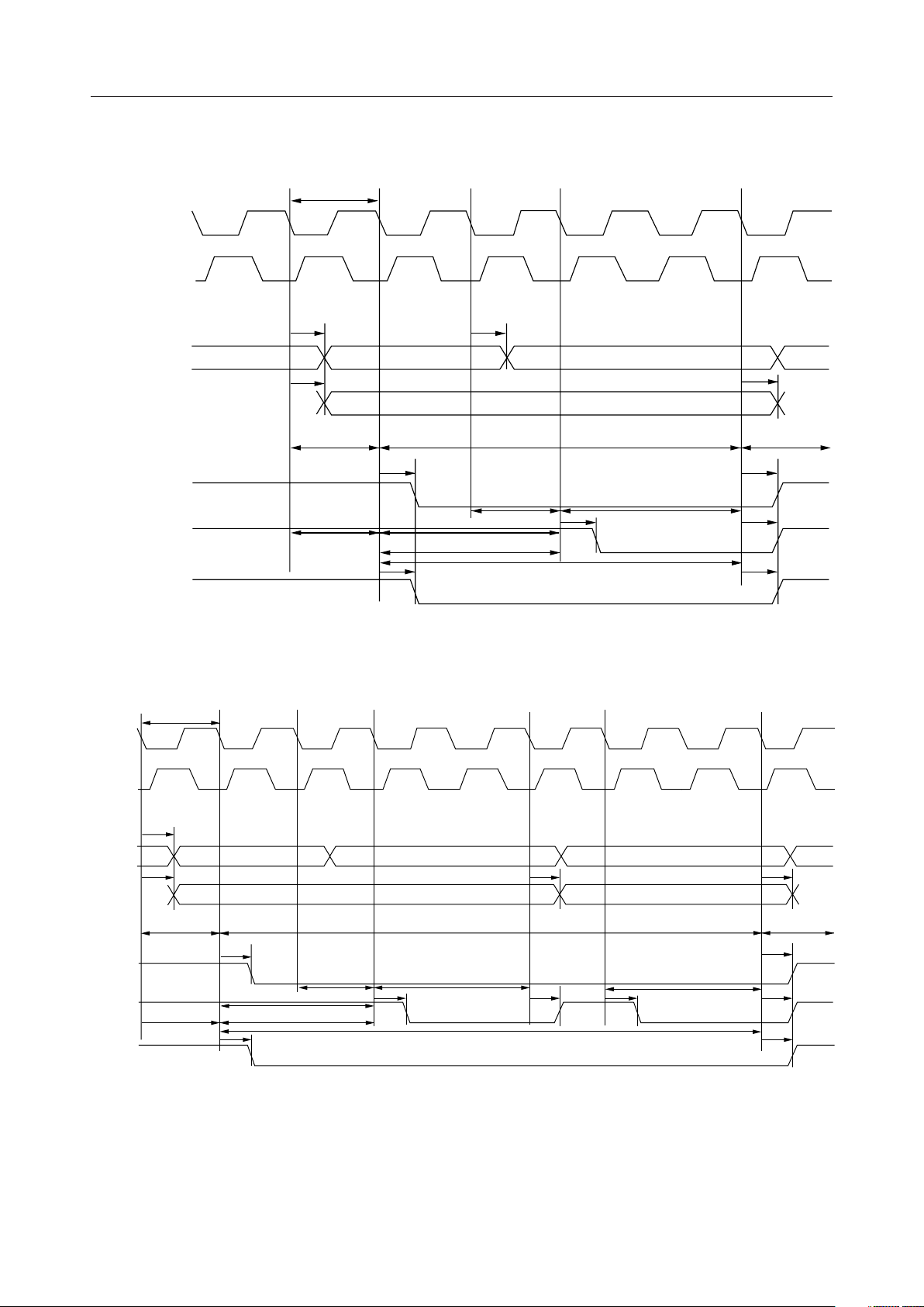
CLK
CLKA
t
MSM7630¡ Semiconductor
OSC
CLK
RAS
CAS
WE
D
A
t
OSC
t
A
t
A
row address column address
t
D
t
W_ARAS
t
RAS
t
W_ACAS
t
W_AWE
tt
3n
t Access (Fast Page Mode/Hyperpage Mode)
tt
t
W_RASCAS
t
W_WECAS
t
WE
t
W_RAS
t
CAS
t
W_CAS
t
W_PREC
t
RAS
t
t
CAS
t
D
WE
CLKA
RAS
CAS
WE
t
A
A
t
D
D
t
W_ARAS
t
W_AWE
row address
t
RAS
t
W_RASCAS
t
W_CAS
t
WE
3n
t Access (Fast Page Mode/Hyperpage Mode)
t
W_ACAS
tt
tt
column address column address
t
D
t
W_RAS
t
CAS
t
W_CAS
t
W_WE
t
CAS
t
CAS
t
W_CAS
t
CAS
t
t
t
RAS
WE
t
D
W_PREC
20/95
Page 21
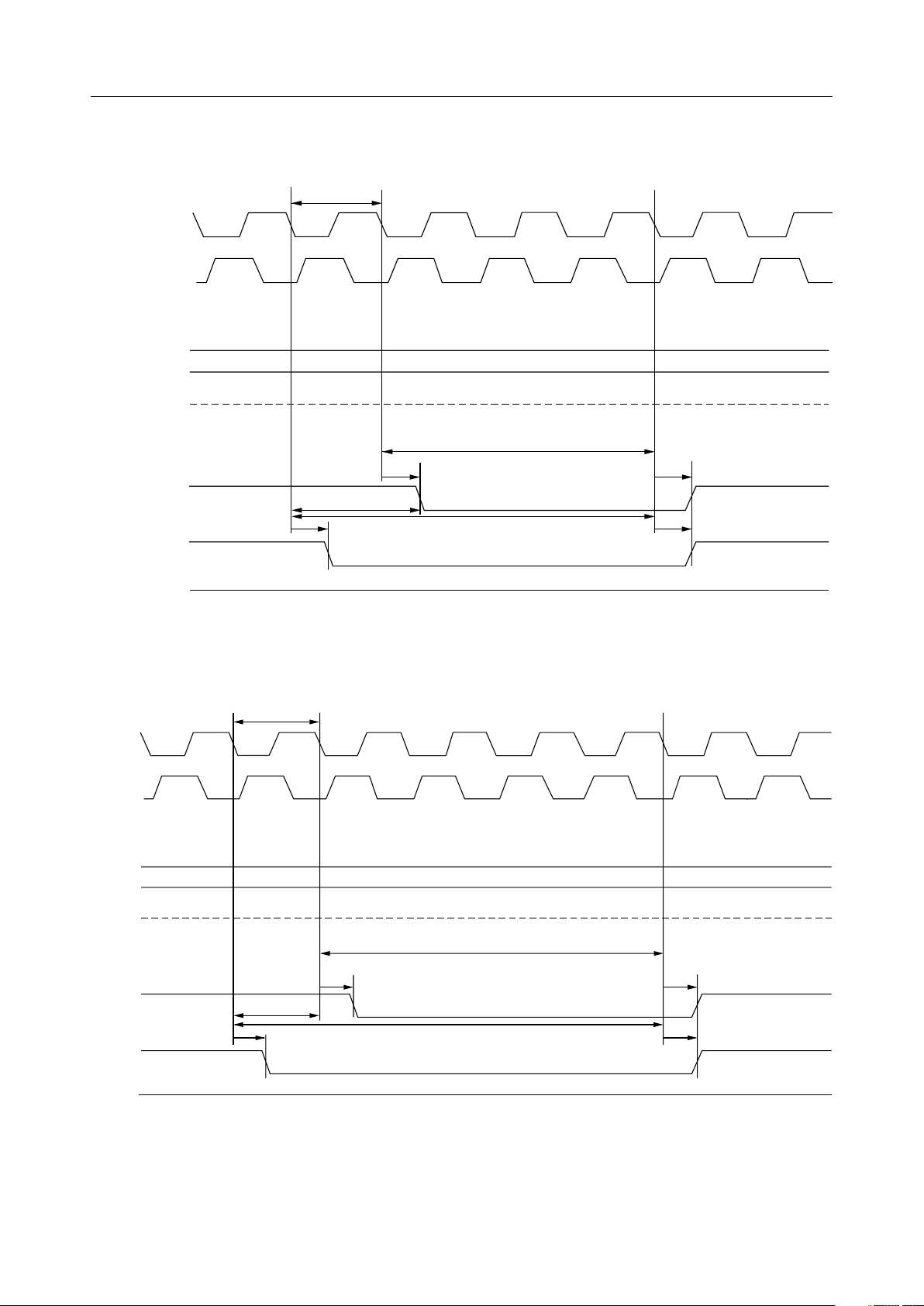
DRAM Refresh
CLK
CLKA
t
OSC
MSM7630¡ Semiconductor
CLK
CLKA
RAS
CAS
WE
A
D
t
RAS
t
W_CASRAS
t
CAS
tt
2n
t CAS-Before-RAS Refresh
tt
t
OSC
ignore
ignore
t
W_RAS
t
W_CAS
t
RAS
t
CAS
RAS
CAS
WE
A
D
t
RAS
t
W_CASRAS
t
CAS
tt
3n
t CAS-Before-RAS Refresh
tt
ignore
ignore
t
W_RAS
t
W_CAS
t
RAS
t
CAS
21/95
Page 22
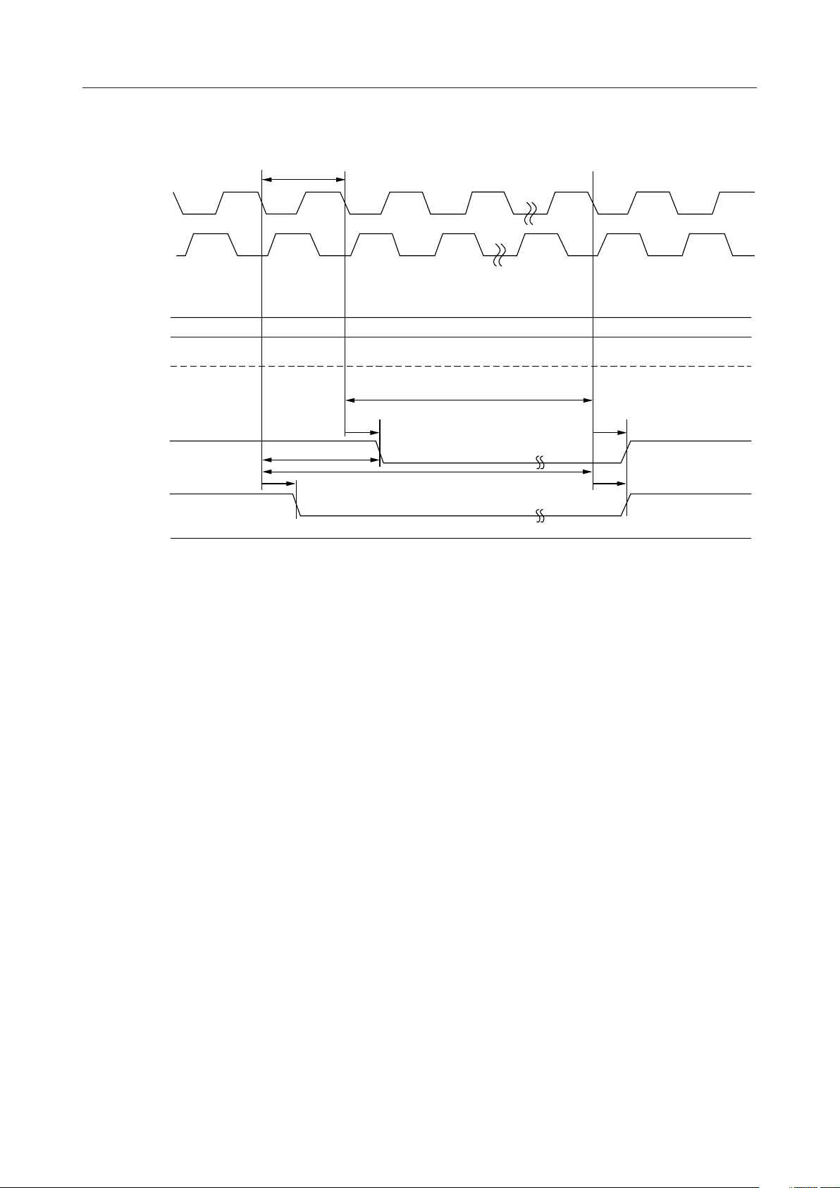
CLK
CLKA
t
OSC
MSM7630¡ Semiconductor
RAS
CAS
WE
A
D
t
RAS
t
W_CASRAS
t
CAS
ignore
ignore
t
W_RAS
t
W_CAS
t
RAS
t
CAS
CAS-Before-RAS Self-Refresh
22/95
Page 23
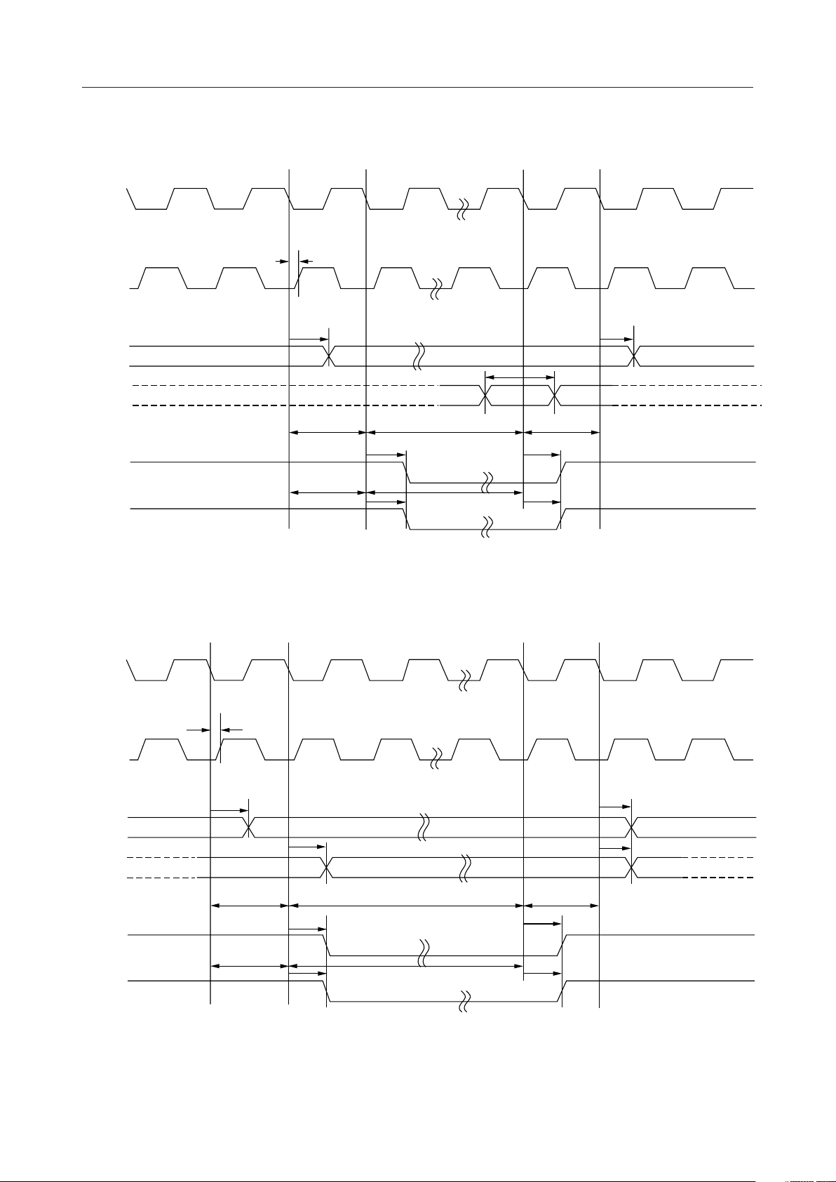
General Device Access
CLK
CLKA
t
CLKA
MSM7630¡ Semiconductor
AS
RD
CLK
CLKA
t
A
t
A
A
t
S_D
t
H_D
D
t
W_AAS
t
W_ARD
t
W_AS
t
AS
t
W_RD
t
RD
t
t
AS
W_AAS
t
RD
Bus Read
t
CLKA
AS
WR
t
t
A
A
A
t
D
t
D
D
t
W_WR
t
W_AS
t
W_AAS
t
t
AS
WR
t
W_AAS
t
W_AWR
t
AS
t
WR
Bus Write (When DS bit in the SCR register is "0")
23/95
Page 24
CLK
CLKA
t
CLKA
MSM7630¡ Semiconductor
WR
CLK
CLKA
AS
t
A
t
A
A
t
D
t
D
D
t
W_AAS
t
W_AWR
t
AS
t
W_DWR
t
W_AS
t
W_WR
t
WR
t
W_AAS
t
AS
t
WR
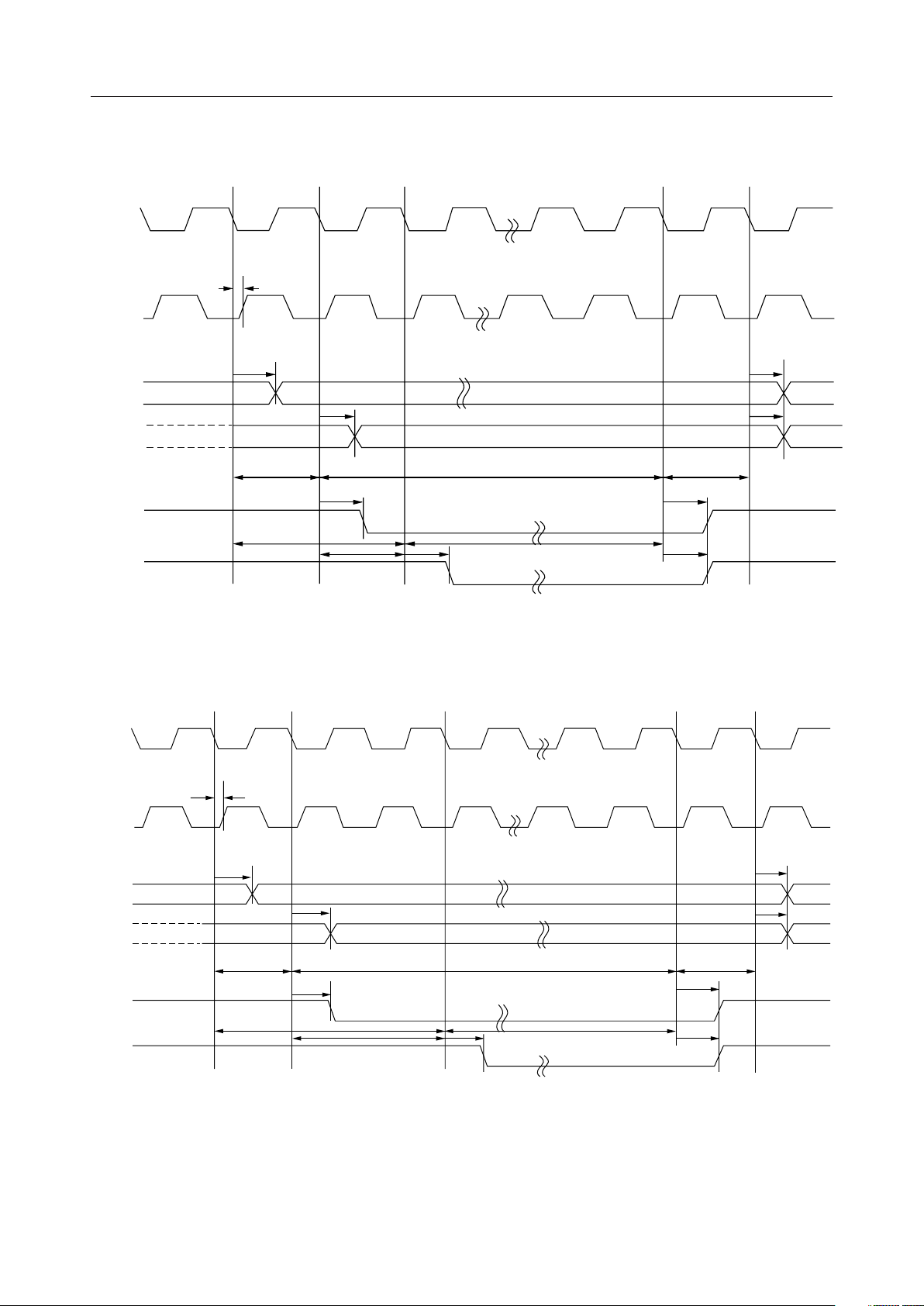
Bus Write (When DS bit is "1" and X bit is "0" in the SCR register)
t
CLKA
AS
WR
t
t
A
A
A
t
D
t
D
D
t
W_AAS
t
W_AWR
t
AS
t
W_DWR
t
W_AS
t
WR
t
W_WR
t
W_AAS
t
AS
t
WR
Bus Write (When DS bit is "1" and X bit is "1" in the SCR register)
24/95
Page 25
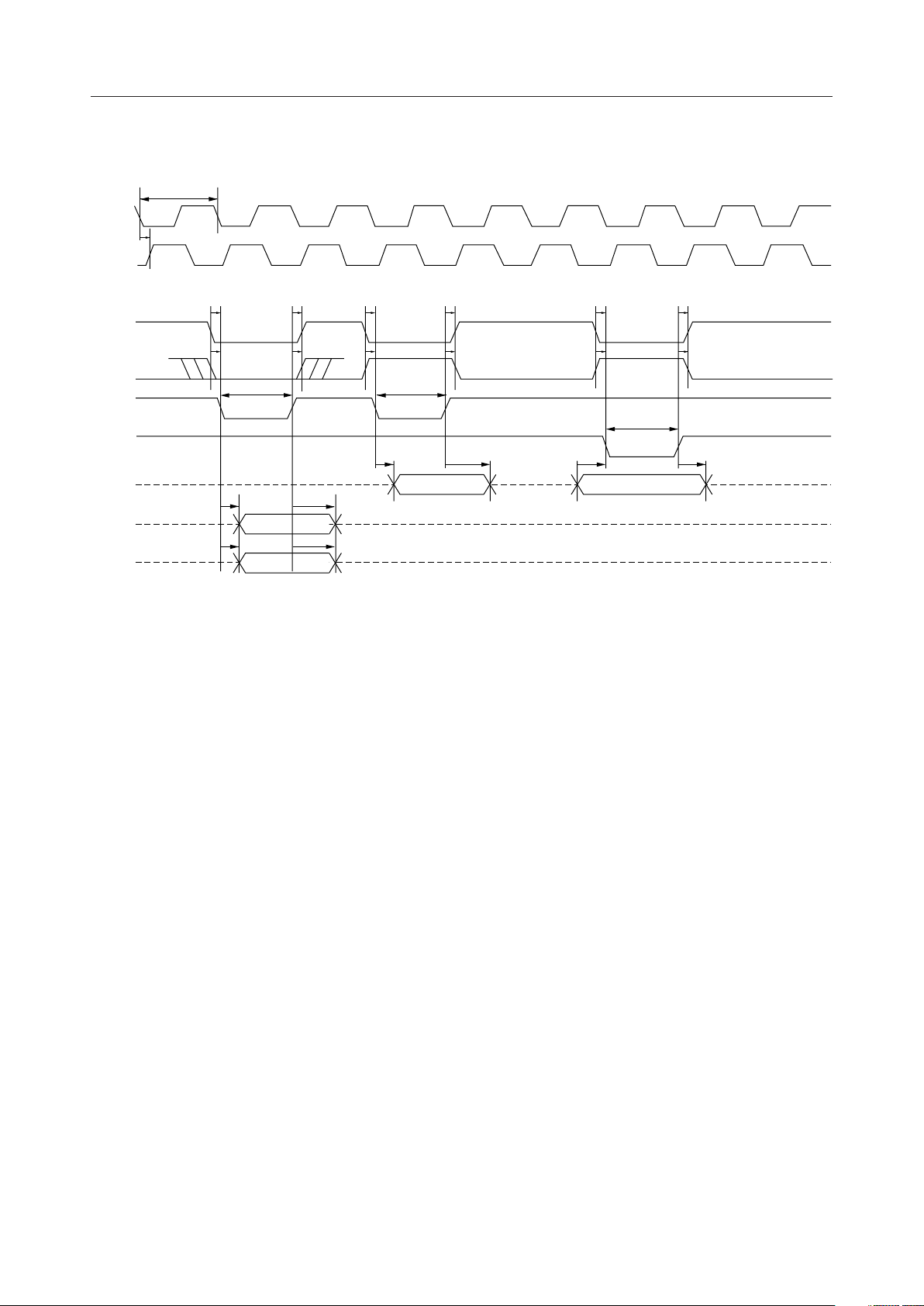
Parallel Interface
t
OSC
CLK
t
CLKA
CLKA
MSM7630¡ Semiconductor
PCS
PIOA
PACK
PSTB
PD
PIBF
POBF
t
S_PCS
t
S_PIOA
t
W_PACK
t
PACK
t
PACK
t
H_PCS
t
H_PIOA
t
PACK
t
PRDZ
t
PRDZ
t
S_PCS
t
S_PIOA
t
W_PACK
t
PRDZ
t
H_PCS
t
H_PIOA
t
S_PD
t
S_PCS
t
S_PIOA
t
W_PSTB
t
H_PCS
t
H_PIOA
t
H_PD
25/95
Page 26
MSM7630¡ Semiconductor
26/95
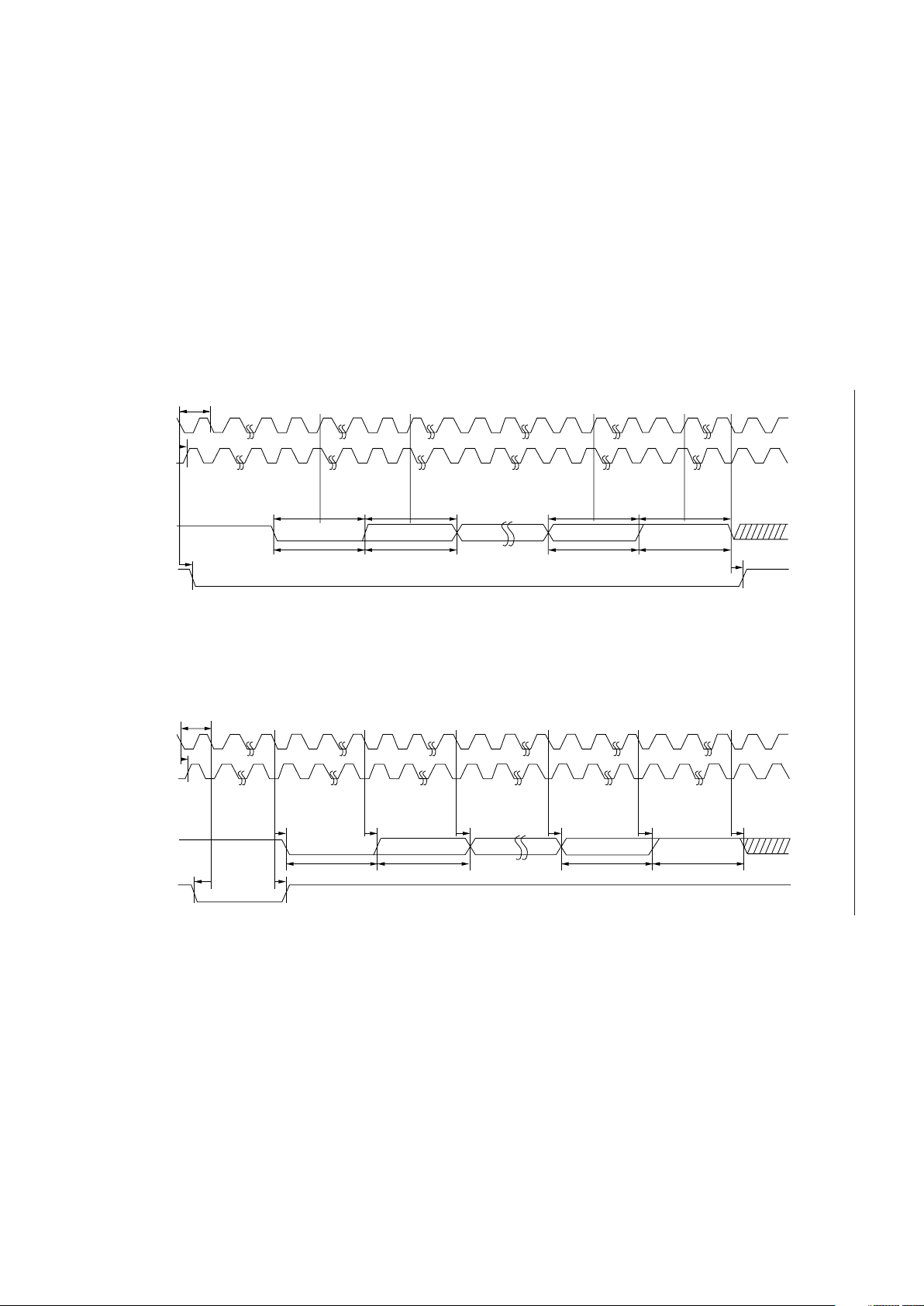
Serial Interface
CLK
CLKA
RXD
RTS
t
OSC
t
CLKA
t
RTS
t
H_RXD
t
S_RXD
t
W_RXD
t
W_RXD
bit 7 Stop_bit (= 1)
t
H_RXD
t
S_RXD
bit 6bit 1bit 0Start_bit (= 0)
t
H_RXD
t
S_RXD
t
H_RXD
t
S_RXD
t
W_RXD
t
W_RXD
t
RTS
bit 6bit 1
bit 0
Stop_bit (= 1)bit 7
Start_bit (= 0)
t
TXD
t
TXD
t
TXD
t
TXD
t
TXD
t
TXD
t
W_TXD
t
W_TXD
t
W_TXD
t
W_TXD
t
H_CTS
t
S_CTS
t
OSC
t
CLKA
CLK
CLKA
TXD
CTS
Page 27
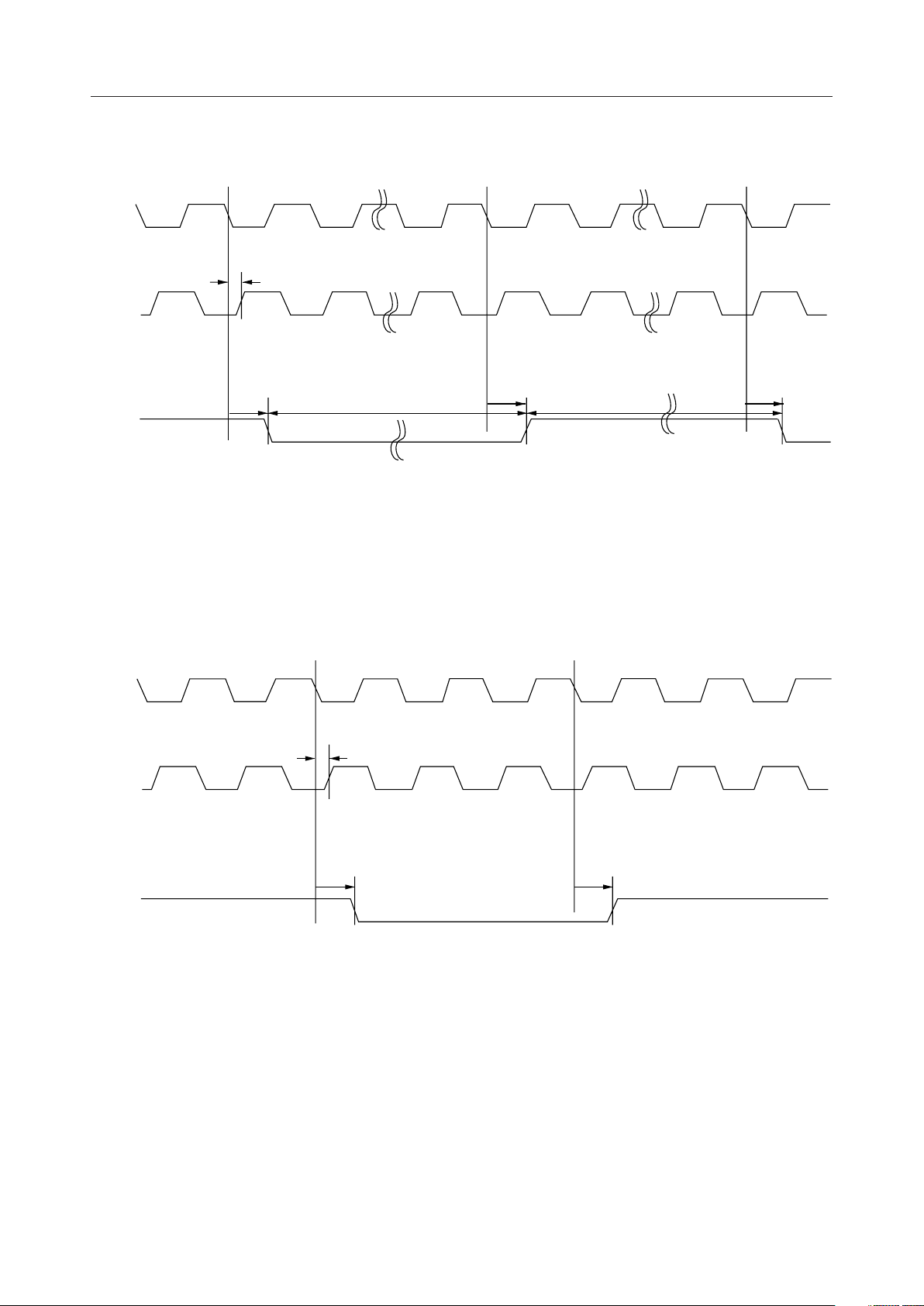
CLK
CLKA
t
CLKA
MSM7630¡ Semiconductor
t
SCLK
SCLK
General Port Output
CLK
CLKA
t
t
W_SCLK
SCLK
Synchronous Transfer Output
t
CLKA
t
W_SCLK
t
SCLK
UPORT
t
UPORT
General Port Output
t
UPORT
27/95
Page 28
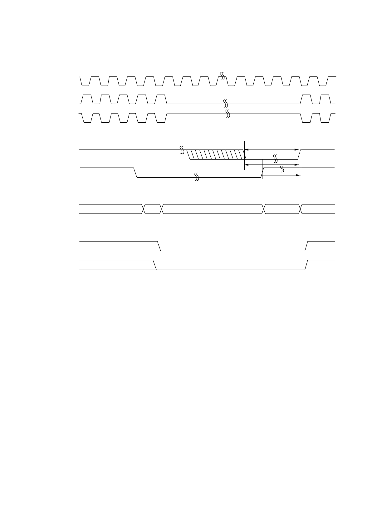
Standby Operation
CLK
XO
CLKA
RST*
STBY
t
RSTSTBY_S
t
W_RST
MSM7630¡ Semiconductor
t
RSTSTBY_H
t
STBYCLKA
CPU Operation
Operating
Suspend
Process
Suspend Resume Process Operating
RAS
CAS
Maintain the pin level on the STBY signal until the CPU has completed its suspend process and clock
signal CLKA has stopped.
After the STBY signal is released, the CPU will not resume until oscillation has stabilized (1024 t
CYC
* The RST signal is not necessary for self-refresh DRAM.
).
28/95
Page 29
MSM7630¡ Semiconductor
Interrupt Process
CLK
XO
CLKA
EXTINT
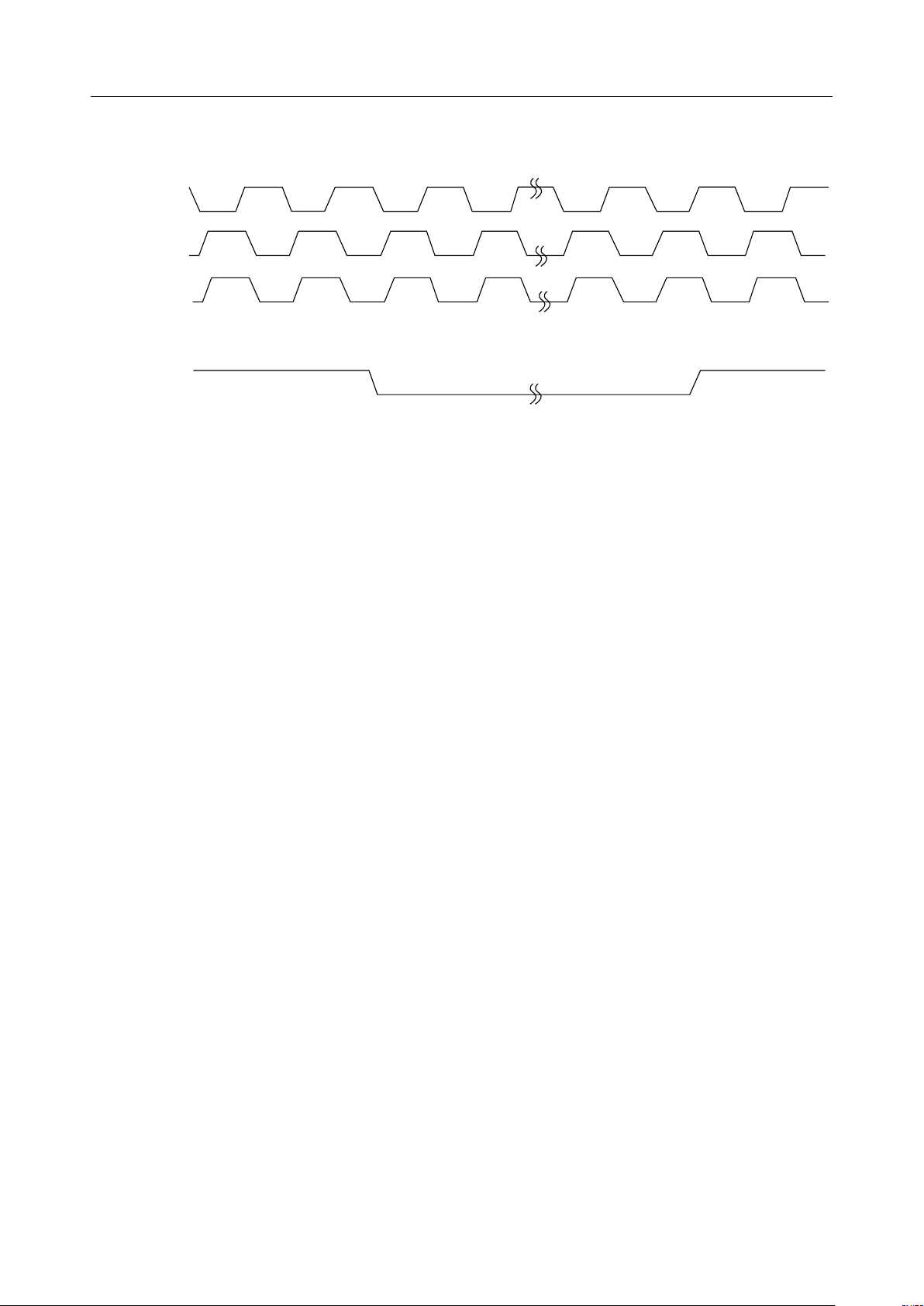
The external interrupt signal EXTINT requests an interrupt to the CPU. The pin level on EXTINT
must be maintained until the CPU accepts the interrupt. Also, be sure to clear the interrupt source
within the interrupt routine.
29/95
Page 30
MSM7630¡ Semiconductor
FUNCTIONAL DESCRIPTION
CPU Core
1. Features
The SCP (Speech Control Processor) uses a CPU core with an Oki-original 32-bit RISC architecture.
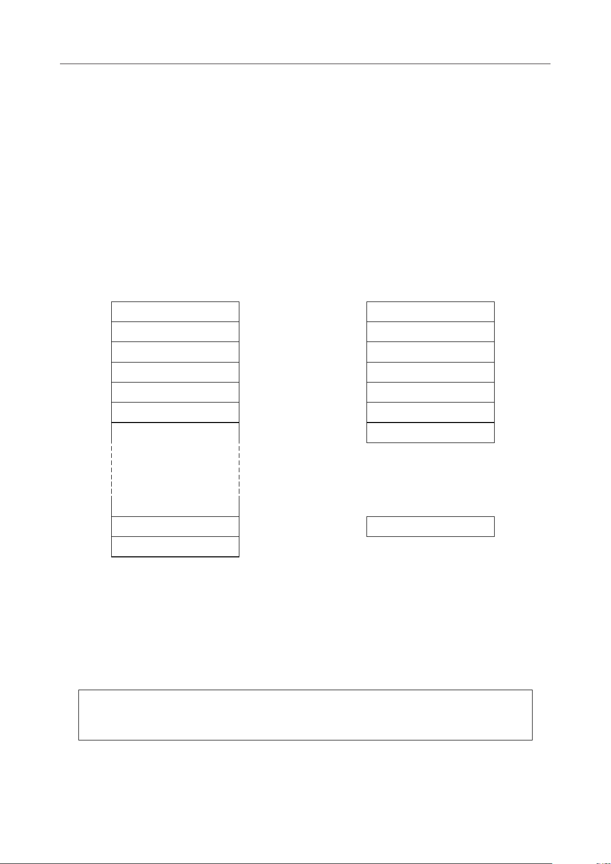
2. Register Configuration
The CPU core registers are configured as 32 words for general registers, 7 words for privileged
registers, and 1 word for a special register.
General Registers
%r0 (link)
%r1 (pre-PC)
%r2 (pre-nPC)
%r3 (long-immed.)
%r4
%r5
%r30
%r31
Privileged Registers
%PSR
%VBA
%prPSR
%IRR
%BPA
%PC
%nPC
Special Register
%NOP
2.1 General Registers
The general registers are a set of 32 registers with 32-bit width. Of these registers %r0 to %r3 can be
used as general registers, but they do have special functions pre-assigned by the system. Registers
%r4 to %r31 can be used freely. Contents are undefined after reset.
bit 31 0
GR
30/95
Page 31
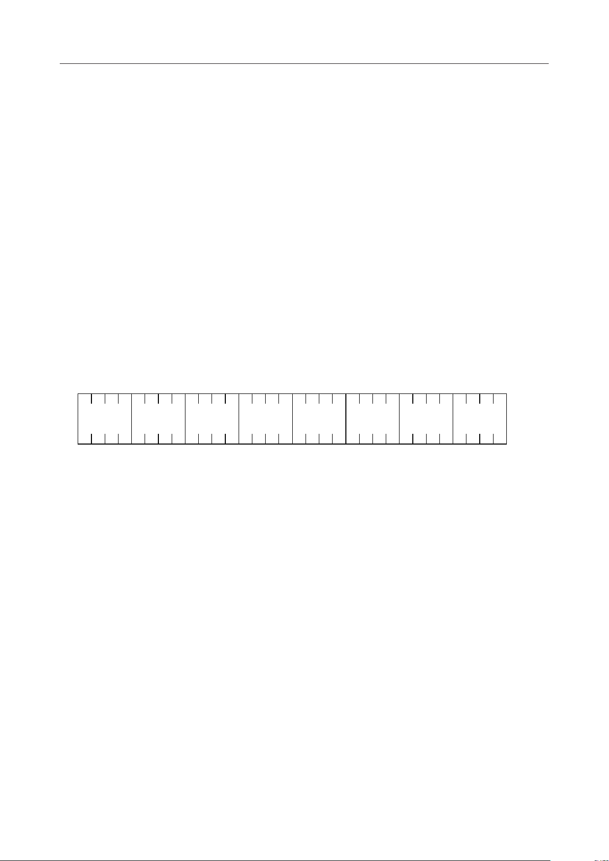
MSM7630¡ Semiconductor
%r0: Link register (stores subroutine return address). Also stores %PC+4 during bl instruction
execution.
%r1: Stores value of %PC when an exception, interrupt, or trap is accepted.
%r2: Stores value of %nPC when an exception, interrupt, or trap is accepted.
%r3: Stores the immediate value of SETLI (Set Long Immediate) instructions.
2.2 Privileged Registers
Reads are allowed at any processor level (Processor Level: 0 = user mode, 1 or above = supervisor
mode), but write accesses are allowed only when the processor level is supervisor mode. The
privileged registers are configured as 7 words, and are used primarily for processor control. If the
processor attempts a write access to a privileged register while in user mode, then the instruction will
not be executed and a privileged instruction exception will be issued.
2.2.1 PSR (Processor Status Register)
This register sets and displays the state of the processor.
31 28 27 26 25 24
bit
VER
0000
23 22 21 20
M
M
F
F
0
U
U
32
16
19 18 17 16
0
0000
15 14 13 12
VCNZ
11 10 9 8
I
0IC
C
P
L
7 6 5 4
N
O
00EB
P
P
3 0
E
M
PL
• bit[31:28] VER: Version (read-only)
Indicates the CPU core version. Currently fixed to "3".
• bit[22] MFU32 (read-only)
Indicates whether the 32-bit multiplier unit is present ("1") or not ("0"). This is "0" for the MSM7630.
• bit[21] MFU16 (read-only)
Indicates whether the 16-bit multiplier unit is present ("1") or not ("0"). This is "1" for the MSM7630.
• bit[15] V: Overflow (read-only)
Indicates that execution of an addition or subtraction instruction resulted in an arithmetic
overflow.
• bit[14] C: Carry (read-only)
Indicates that execution of an addition or subtraction instruction resulted in an arithmetic carry or
borrow.
• bit[13] N: Negative (read-only)
Indicates that execution of an addition or subtraction instruction resulted in a negative value
(bit[31] is "1").
31/95
Page 32

MSM7630¡ Semiconductor
• bit[12] Z: Zero (read-only)
Indicates that execution of an addition or subtraction instruction resulted in a zero value (bit[31:0]
are all "0").
• bit[10] ICP: Instruction Cache Purge (read/write)
Invalidates all instruction cache entries. Writing "1" to this bit purges the contents of the instruction
cache. After this process (after one cycle) this bit is automatically cleared to "0" by hardware. The
instruction cache is purged during reset.
• bit[9] ICL: Instruction Cache Lock (read/write)
Freezes all instruction cache entries. After "1" is written to this bit, instruction cache contents are
frozen and then instruction execution continues. This bit will be "1" after reset.
• bit[8] NOP: Non-Operation (read-only)
When set to "1", forces the next instruction to a NOP regardless of the instruction. There is no way
to directly set this bit to "1". This bit will be "0" after reset.
• bit [5] EBP: Breakpoint Trap Enable (read/write)
Enables breaks. If this bit is set to "1", then a trap will occur when the value of the instruction
execution address (%PC) equals the value of the breakpoint address (%BPA). The instruction that
generated the break will not be executed. This bit will be "0" after reset.
• bit[4] EM: Master Enable (read/write)
Disables all exceptions, interrupts, and traps. This bit automatically becomes "0" at the point when
the processor accepts an exception, interrupt, or trap. While this bit is "0", further exceptions,
interrupts or traps will not be accepted, with instruction execution continuing in the normal
instruction sequence. An instruction must be used to return this bit to "1". It will be "0" after reset.
• bit[3:0] PL: Processor Level (read/write)
Sets and provides the processor’s instruction execution level. Processor levels are 0-15. An external
interrupt will be accepted if its level has a higher priority than the processor level at that time.
External interrupt levels are 1-16, so when PL is 0 all external interrupts will be accepted, and when
PL is 1 external interrupts of level 2 and above will be accepted. When an external interrupt is
accepted, the processor level will become the same as the external interrupt level. For example, if
PL is 5 and a level 7 external interrupt is accepted, then PL will transition to 7 at that point. When
PL is restored to its previous state, its saved value in %prPSR will be restored to %PSR.
Alternatively PL can be set to its previous value explicitly by an instruction in the interrupt process
routine. However, %PSR is a privileged register, so writes are only permitted in supervisor mode.
PL will be set to 15 after reset.
32/95
Page 33
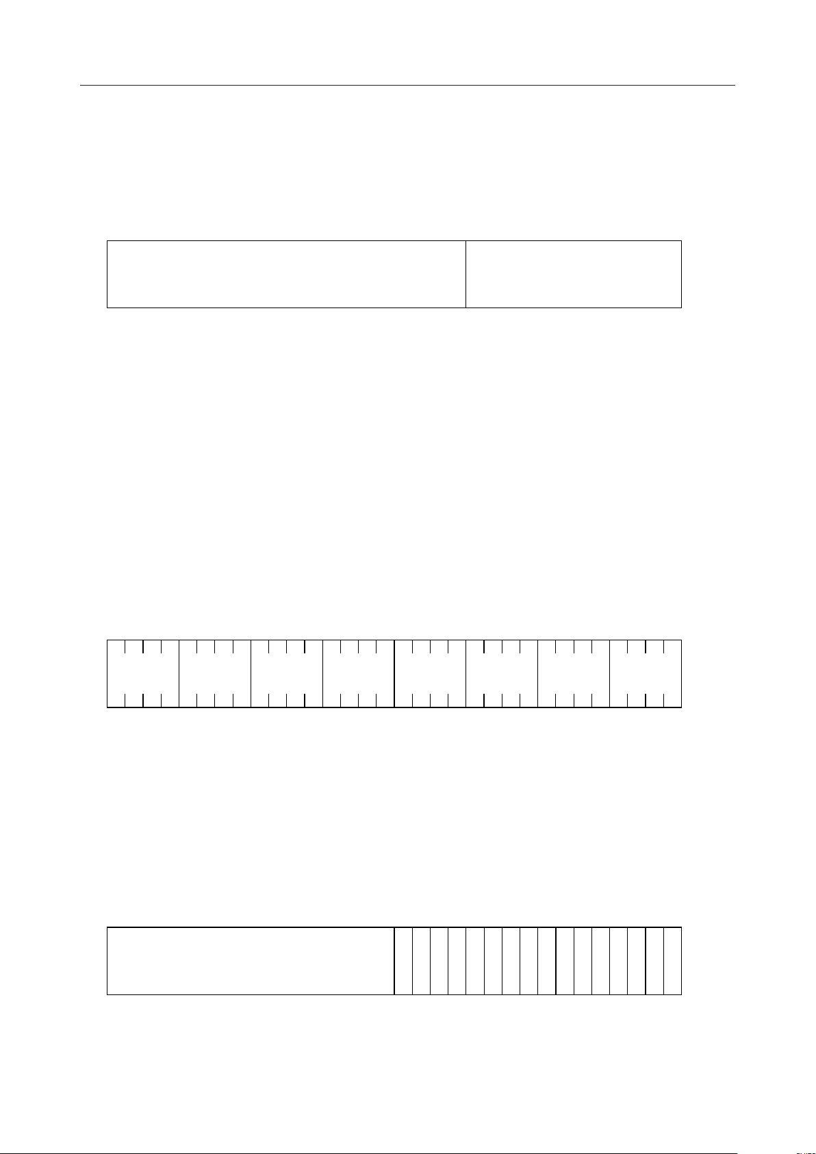
MSM7630¡ Semiconductor
2.2.2 VBA: Vector Base Address (read/write)
This read/write register sets the leading address of the dispatch table (vector table) to exception,
interrupt, and trap process routines.
31 12 11
00
0000000000VBA
0bit
The dispatch table is 256 entries of 4K bytes size, with 16 bytes (4 instructions) save for each entry’s
dispatch routine. Entry points are generated by an OR operation with this register, so they are set
at 4K-byte boundaries. As a result, only the upper 20 bits of an argument will be written to the VBA
register (the lower 12 bits will be ignored).
Entry_point = VBA[31:12] ÍÍ(vector_number << 4)
This register is undefined after reset.
2.2.3 prPSR: Pre-Processor Status Register (read/write)
This read/write register saves the value of %PSR at the time an exception, interrupt, or trap is
accepted. In order to accept overlapping exceptions, interrupts, and traps, the value of %prPSR must
be pushed on a stack and then EM of %PSR must be set to "1".
31 28 27 26 25 24
bit
VER
0000
23 22 21 20
M
M
F
F
0
U
32
16
0
U
19 18 17 16
0000
15 14 13 12
pVpCpNp
Z
11 10 9 8
p
p
I
I
0
C
C
P
L
7 6 5 4
p
N
00
O
P
p
E
B
P
3 0
p
E
M
pPL
The upper 16 bits of %prPSR are always identical to %PSR. Refer to the descriptions of the same bit
positions in %PSR for an explanation of %prPSR bits.
2.2.4 IRR: Interrupt Request Register (read-only)
This register indicates whether there is an interrupt request at each of the 16 levels of external
interrupts. It is read-only, and shows interrupt requests regardless of PL (processor level). The IRR
value will continue until an interrupt source is released.
31 12 11
I
I
R
Q
15
R
Q
14
R
Q
13
I
R
Q
12
0000000000000000
N
M
I
I
I
I
I
I
I
I
10
R
R
R
Q
Q
Q
8
9
R
Q
11
I
R
R
R
Q
Q
Q
7
6
5
1234567891013141516
0bit
I
I
I
I
R
R
R
R
Q
Q
Q
Q
4
3
2
1
33/95
Page 34
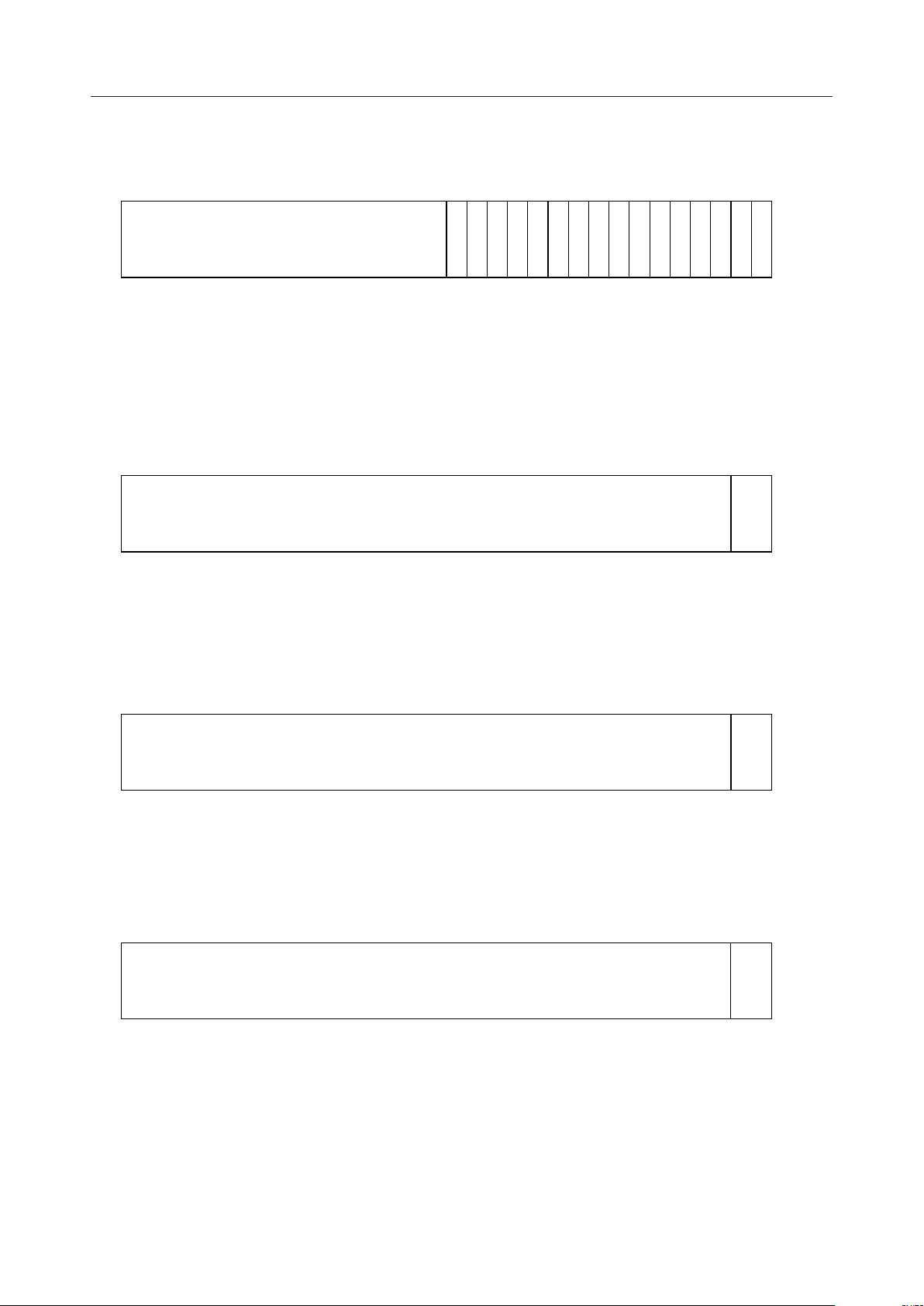
The MSM7630 uses only 6 interrupts of the 16 interrupt levels.
MSM7630¡ Semiconductor
31 12 11
00000000000000000000
0
R
Q
11
I
I
I
I
R
R
0
0
Q
9
R
0
Q
Q
7
5
1234567891013141516
0bit
I
R
0
00
Q
3
2.2.5 BPA: Breakpoint Address (read/write)
This read/write register sets and shows the instruction address (byte address) where a breakpoint
trap occurred. The lowest 2 bits will always be "0". When EBP of %PSR is "1", a trap will be generated
immediately before execution of the instruction at the breakpoint set by this register. This register
will be undefined after reset.
31 0bit
BPA
12
00
2.2.6 PC: Program Counter (read-only)
This read-only register provides the instruction address (byte address) in the execution phase. Its
lowest 2 bits will always be "0".
31 0bit
PC
12
00
2.2.7 nPC: Next Program Counter (read-only)
This read-only register provides the instruction address (byte address) in the instruction decode
phase. Its lowest 2 bits will always be "0".
31 0bit
nPC
12
00
34/95
Page 35
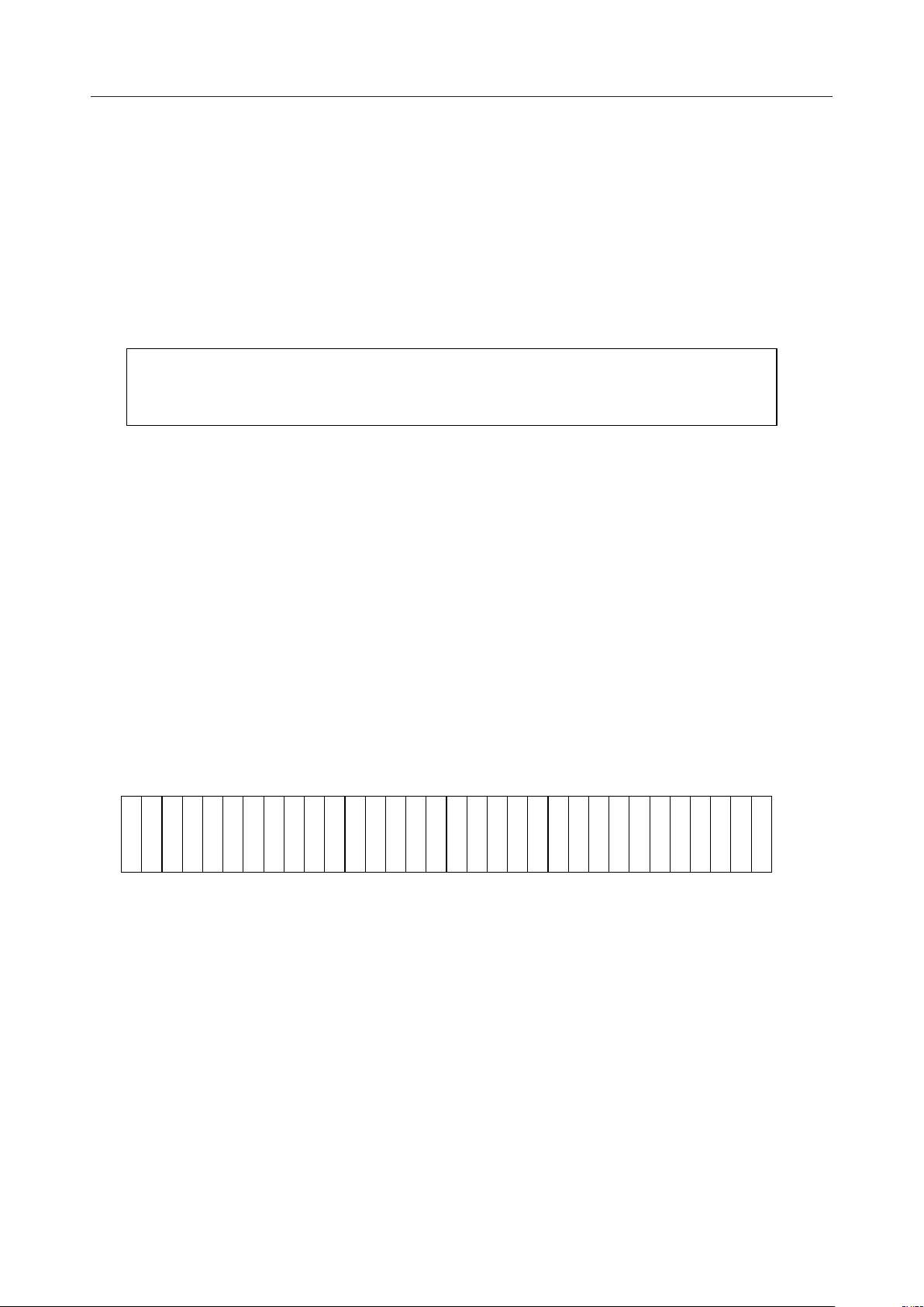
MSM7630¡ Semiconductor
2.3 Special Registers
These are not privileged registers, but they are special registers used for specific functions.
2.3.1 NOP: Non-Operation (read/write)
When this register is specified as a destination register, execution results will not be stored anywhere.
When specified as a source register, it will read as an undefined value.
31 0bit
NOP
3. Data Formats
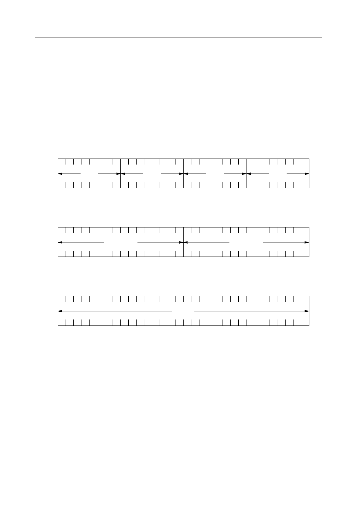
There are two data format types: one for internal processor core calculations and one for memory
accesses.
3.1 Internal Data Format
The CPU core handles all data as 32 bits (word format). Therefore, when the format of data stored
in memory is byte (8 bits) or half-word (16 bits) it must be used internally as 32-bit data through a
signed load instruction or unsigned load instruction. Similarly when internal core processing results
are stored to memory, a store instruction corresponding to the data format in memory must be
executed. Also, bit addresses specified for bit test instructions and bit manipulation instructions are
shown in the diagram below.
31 0bit 123456789101112131415161718192021222324252627282930
35/95
Page 36
MSM7630¡ Semiconductor
3.2 Memory Data Format
The following memory data formats are supported: byte (8 bits), half-word (16 bits), and word (32
bits). Memory addresses are always byte addresses regardless of data format. However, half-word
accesses must be on 16-bit boundaries (least significant bit is "0"), and word accesses must be on 32bit boundaries (least significant 2 bits are "00"). If a load or store instruction execution attempts a
memory access that violates these boundaries, then a data address invalid exception will occur.
Memory addressing is big-endian. The diagrams below show memory data formats for byte data
access, half-word data access, and word data access.
Byte Data Access
31 24
byte
Half-Word Data Access
31
Word Data Access
31 0bit
23 16 15 8 7 0bit
byte byte byte
n n+1 n+2 n+3Address
16 15 0bit
half word
nAddress
word
half word
n+1
nAddress
36/95
Page 37

MSM7630¡ Semiconductor
3.3 Memory Addressing Modes
Memory addresses are byte addresses, so memory addressing is performed with three types of load
instructions and two types of store instructions. Swap instructions have the same memory
addressing as store instructions.
3.3.1 Load Instruction Addressing
1. Base + Index
The effective address (EA) is obtained by adding the values of any two general registers %r0-31
specified.
EA = [reg_S1 + reg_S2]
2. Base + Displacement
The effective address (EA) is obtained by adding the value of any general register %r0-31 specified
and a displacement given by the instruction’s immediate value field.
EA = [reg_S1] + offS
3.3.2 Store Instruction Addressing
1. Base + Displacement
The effective address (EA) is obtained by adding the value of any general register %r0-31 specified
and a displacement given by the instruction’s immediate value field.
EA = [reg_S1] + offS
37/95
Page 38

4. Instruction Set
All instructions are fixed 32-bit length.
MSM7630¡ Semiconductor
Category Instruction
Unconditional branch
Conditional branch
Bit test
Comparison
Trap
Arithmetic/logical operation
Extend
Shift
Bit manipulation
Function
b{,x}?
bl{,x}?
bt{,x/t} S1,? Conditional Branch
bf{,x/t} S1,?
jlr {,x} S2,D*
jlrt {,x/t} S1,S2,D*
jlrf {,x/t} S1,S2,D* Conditional branch to subroutine
rt S2
btst1 S1,S2/immU,D Bit test
btst0 S1,S2/immU,D
cmpeq S1,S2/immS,D
cmple S1,S2/immS,D
cmplt S1,S2/immS,D
cmpls S1,S2/immS,D
cmpc S1,S2/immS,D
cmpne S1,S2/immS,D
cmpgt S1,S2/immS,D
cmpge S1,S2/immS,D
cmphi S1,S2/immS,D
cmpnc S1,S2/immS,D
trap vct
add S1,S2/immS9,D
sub S1,S2/immS9,D
adc S1,S2/immS9,D
sbc S1,S2/immS9,D
and S1,S2/immS9,D
or S1,S2/immS9,D
xor S1,S2/immS9,D
sbr S1,S2/immS12,D
extu S1,S2/immU,D
ext S1,S2/immU,D
sl S1,S2/immS,D
rot S1,S2/immS,D
slr S1,S2/immS,D
sar S1,S2/immS,D
brst S1,S2/immU,D
bset S1,S2/immU,D
bnot S1,S2/immU,D
brst %psr,4/5,%psr
brst %psr,4/5,%psr
Unconditional branch
Unconditional branch to subroutine
Conditional Branch
Conditional branch to subroutine
Conditional branch to subroutine
Return from subroutine
Bit test
Comparison [=]
Comparison [signed: £]
Comparison [signed: <]
Comparison [unsigned: £]
Comparison [unsigned: <]
Comparison [π]
Comparison [signed: >]
Comparison [signed: ≥]
Comparison [unsigned: >]
Comparison [unsigned: ≥]
Transfer to trap toutine
Add
Subtract
Add with carry
Subtract with carry
Logical AND
Logical OR
Exclusive OR
Subtract
MSB extend
MSB extend
Logical shift
Logical rotate
Logical shift
Arithmetic shift
Set bit to "0"
Set bit to "1"
Invert bit
Set bit to "0"
Set bit to "1"
38/95
Page 39

MSM7630¡ Semiconductor
Category Instruction
Register-register move
Store immediate value
Store
Swap
Load
Multiplication
Function
mov S,D
movh S1,D'
seti imm17S,D Store immediate value
setih const16,D'
setli const25
sb S2/immS,[S1+offS] Byte store
shw S2/immS,[S1+offS]
sw S2/immS,[S1+offS]
swap S2,[S1+offS]
lb [S1+offS],D'
lhw [S1+offS],D'
lw [S1+offS],D'
mul0 S1,S2/immS,D'
mul16 S1,S2/immS,D'
mul32 S1,S2/immS,D'
mulu0 S1,S2/immS,D'
mulu16 S1,S2/immS,D'
mulu32 S1,S2/immS,D'
Move
Move upper bits
Store immediate value to upper 16 bits
Store immediate value left-shifted 7 bits to %r3
Half-word store
Word store
Swap
Byte load
Half-word load
Word load
Signed multiply
Signed multiply
Signed multiply
Unsigned multiply
Unsigned multiply
Unsigned multiply
Multiply instructions need two clocks for execution time.
The MSM7630 can only use the mul0 and mulu0 instructions of the multiplication instructions.
39/95
Page 40

MSM7630¡ Semiconductor
5. Exceptions, Traps, and Interrupts
The CPU core of SCP provides error exceptions, traps, external interrupts, and software traps (by
trap instructions). Each type has a corresponding interrupt priority level and instruction dispatch
address.
Source Vector
Number
System reset
CPU reset (INIT) 0
Instruction access exception 1
Instruction address invalid exception 2
Reserved instruction exception 3
Privileged instruction exception 4
Data address invalid exception 5
Data access exception 6
Reserved 7
Breakpoint trap 8
Reserved 9
to 32
External interrupt 1 33
External interrupt 2 34
External interrupt 3 35
External interrupt 4 36
External interrupt 5 37
External interrupt 6 38
External interrupt 7 39
External interrupt 8 40
External interrupt 9 41
External interrupt 10 42
External interrupt 11 43
External interrupt 12 44
External interrupt 13 45
External interrupt 14 46
External interrupt 15 47
External interrupt 16 (NMI) 48
TRAP instruction 0
to 255
The system reset vector is at absolute address 0. All others are ORed with VBA as the base address.
Branch Address
0x00000000 0
VBA+0x000
VBA+0x010
VBA+0x020
VBA+0x030
VBA+0x040
VBA+0x050
VBA+0x060
VBA+0x070
VBA+0x080
VBA+0x090
to VBA+0x200
VBA+0x210
VBA+0x220
VBA+0x230
VBA+0x240
VBA+0x250
VBA+0x260
VBA+0x270
VBA+0x280
VBA+0x290
VBA+0x2a0
VBA+0x2b0
VBA+0x2c0
VBA+0x2d0
VBA+0x2e0
VBA+0x2f0
VBA+0x300
VBA+0x000
to VBA+0xff0
Priority Synchronous/Asynchronous
(Sense)
Asynchronous (level)
1
2
3
4
5
8
9
6
25
24
23
22
21
20
19
18
17
16
15
14
13
12
11
10
7
Asynchronous (edge)
Synchronous
Synchronous
Synchronous
Synchronous
Asynchronous (edge)
Asynchronous (edge)
Synchronous
Asynchronous (level)
Asynchronous (level)
Asynchronous (level)
Asynchronous (level)
Asynchronous (level)
Asynchronous (level)
Asynchronous (level)
Asynchronous (level)
Asynchronous (level)
Asynchronous (level)
Asynchronous (level)
Asynchronous (level)
Asynchronous (level)
Asynchronous (level)
Asynchronous (level)
Asynchronous (edge)
Synchronous
Synchronous detection is acceptance of a request within an instruction cycle.
Asynchronous detection is acceptance of a request between instruction cycles or at any point in time
after.
40/95
Page 41

MSM7630¡ Semiconductor
5.1 RST: System Reset
A system reset resets all states under all circumstances.
Type: Asynchronous hardware reset after RST pin level detection.
Vector address: Absolute address 0 (0x00000000).
Conditions: Non-maskable (unconditional)
PL after interrupt transition: 15
5.2 IAE: Instruction Access Exception
An instruction access exception is generated when an instruction is fetched from an undefined
memory space. If the instruction is converted to a NOP by delayed instruction control (x-bit
manipulation), then no exception will be generated.
Type: Instruction-synchronous exception caused by memory access error during instruction fetch.
Vector number/address: Vector number = 1 / VBA+0x010
Conditions: Non-maskable (unconditional). Invalidated by delayed instruction control (x-bit).
Saved address: Address of the instruction that caused the exception.
PL after interrupt transition: 15
5.3 IAIE: Instruction Address Invalid Exception
An instruction address invalid exception is generated when a register indirect branch instruction
attempts an instruction fetch at an address that is not on a word boundary. If the instruction is
converted to a NOP by delayed instruction control (x-bit manipulation), then no exception will be
generated.
Type: Instruction-synchronous exception caused by an illegal JLR or RT instruction.
Vector number/address: Vector number = 2 / VBA+0x020
Conditions: Non-maskable (unconditional). Invalidated by delayed instruction control (x-bit).
Saved address: Address of the instruction that caused the exception.
PL after interrupt transition: 15
41/95
Page 42

MSM7630¡ Semiconductor
5.4 PIE: Privileged Instruction Exception
A privileged instruction exception is generated when an action that can only be performed in
supervisor mode attempted in user mode: (a) in user mode a privileged register is specified as a
destination, or (b) in user mode a number 64 or below is specified for a TRAP instruction vector. If
the instruction is converted to a NOP by delayed instruction control (x-bit manipulation), then no
exception will be generated.
Type: Instruction-synchronous exception caused by an illegal privileged instruction.
Vector number/address: Vector number = 4 / VBA+0x040
Conditions: Non-maskable (unconditional). Invalidated by delayed instruction control (x-bit).
Saved address: Address of the instruction that caused the exception.
PL after interrupt transition: 15
5.5 DAIE: Data Address Invalid Exception
A data address invalid exception is generated when a memory access instruction attempts to access
a memory address not on a word boundary.
Type: Asynchronous exception caused by an illegal memory access instruction.
Vector number/address: Vector number = 5 / VBA+0x050
Conditions: EM == 1. However, exception must be maintained until accepted.
Saved address: Address being executed when the exception was accepted.
PL after interrupt transition: 15
5.6 DAE: Data Access Exception
A data access exception is generated when data is accessed in an undefined memory space.
Type: Asynchronous exception caused by a memory access instruction error.
Vector number/address: Vector number = 6 / VBA+0x060
Conditions: EM == 1. However, exception must be maintained until accepted.
Saved address: Address being executed when the exception was accepted.
PL after interrupt transition: 15
42/95
Page 43

MSM7630¡ Semiconductor
5.7 BPT: Breakpoint Trap
A breakpoint trap is generated when the instruction execution address matches the address pointed
to by the %BPA register. However, the EBP bit in the %PSR register must be enabled. The instruction
at the address that causes the trap will not be executed. The trap will be generated even if the
instruction is converted to a NOP by delayed instruction control (x-bit manipulation).
Type: Instruction-synchronous trap caused by hardware.
Vector number/address: Vector number = 8 / VBA+0x080
Conditions: EM == 1 && EBP == 1. Not invalidated by delayed instruction control (x-bit).
Saved address: Address pointed to by the %BPA register.
PL after interrupt transition: 15
5.8 EINT: External Interrupt 1-15
External interrupts are generated by inputs. However, an external interrupt will be accepted only
when its level has higher priority than the current processor level. When an external interrupt is
accepted, the processor level becomes the same as its level.
Type: Asynchronous interrupt when level on INT1-INT15 pins is detected.
Vector number/address: Vector number = 33-47 / VBA+0x210-0x2f0
Conditions: EM == 1 && PL < external_interrupt_number
Saved address: Address being executed when the interrupt was accepted.
PL after interrupt transition: External interrupt number
The MSM7630 assigns interrupt levels as follows. It does not use other interrupts (including NMI).
Interrupt Source Priority Interrupt Number
User Block/TMR2 1 INT11
External pin (EXTINT) 2 INT9
Serial I/O 3 INT7
Parallel I/O 4 INT5
TMR1 5 INT3
43/95
Page 44

MSM7630¡ Semiconductor
5.9 Return From Interrupt
In order to return from an interrupt process caused by an exception, external interrupt, or software
trap, the pipeline at the time of the interrupt must be regenerated before execution.
There are two types of returns: (1) re-execution of an instruction that was in its execution phase at
the time an exception, external interrupt, or asynchronous trap caused an interrupt, and (2) reexecution of the instruction after the instruction that was in its execution phase at the time a software
trap caused an interrupt. However, if breakpoints are supported by software traps then case (1)
applies.
The return sequence from an interface process is described below.
Also, an rt instruction must not be executed while the EM bit of %PSR is 1 (the state permitting
overlapping interrupts). If an interrupt occurred during the rt instruction in such a case, then the
contents of %PSR would be corrupted.
1. Resume from interrupted instruction
·
·
brst %psr, 4, %psr ; EM-bit reset
jlr %r1, %nop ; delay slot, branch %r1 (old %PC),
; return address not saved
rt %r2 ; return to %r2 (old %nPC), %prPSR move to %PSR
2. Return from instruction after interrupt
·
·
add %r2, 4, %r1 ; %r2+4 (old %nPC+4)Æ%r1
brst %psr, 4, %psr ; EM-bit reset
jlr %r2, %nop ; delay slot, branch %r2 (old %nPC), return address not saved
rt %r1 ; return to %r1 (old %nPC+4), %prPSR move to %PSR
In this case the pNOP bit of %prPSR must be cleared in advance of rt instruction execution. If the
pNOP bit of %prPSR is set and then the rt instruction is executed, then the instruction at the return
point would not be executed.
44/95
Page 45
MSM7630¡ Semiconductor
Bus Interface Unit
1. Features
The SCP’s bus interface unit (BIU) manages address space and outputs control signals that enable
optimal memory access. This allows ROM, SRAM, DRAM and other general devices to be accessed.
2. Address Space
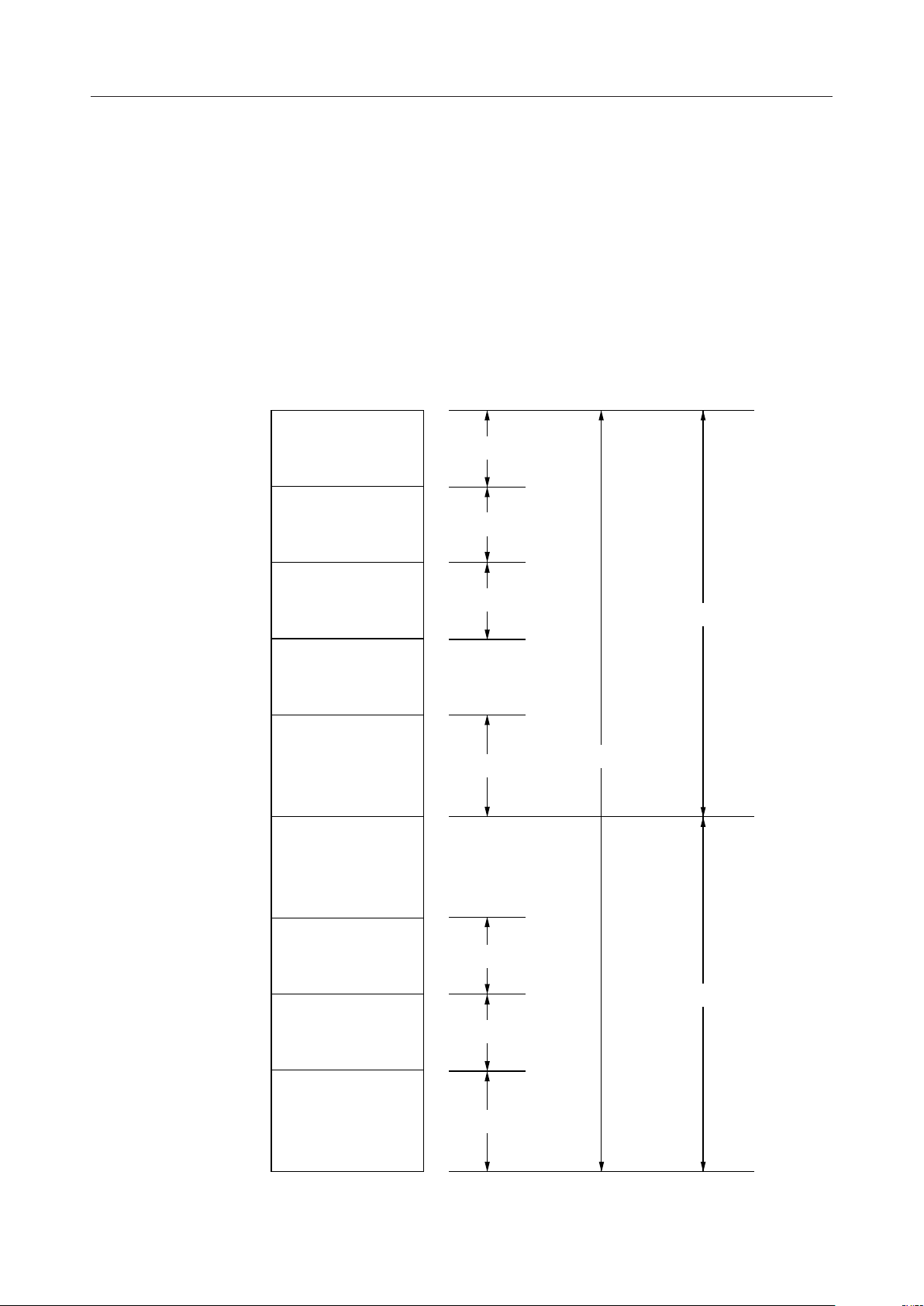
The address space that can be directly accessed by load/store instructions is 4 gigabytes. The BIU
manages this address space by dividing it into several.
0x00000000
0x0FFFFFFF
0x10000000
0x1FFFFFFF
0x20000000
0x2FFFFFFF
0x30000000
0x3FFFFFFF
0x40000000
0x7FFFFFFF
0x80000000
ROM
SRAM
DRAM
Reserved
General devices
Reserved
256 MB
256 MB
256 MB
1 GB
External
4 GB
0xBFFFFFFF
0xC0000000
0xCFFFFFFF
0xD0000000
0xDFFFFFFF
0xE0000000
0xFFFFFFFF
Internal ROM
Internal RAM
Registers
256 MB
Internal
256 MB
512 MB
45/95
Page 46

MSM7630¡ Semiconductor
2.1 ROM Space
ROM space is assigned to 0x00000000-0x0FFFFFFF. When this space is accessed the ROM signal goes
"L".
2.2 SRAM Space
SRAM space is assigned to 0x10000000-0x1FFFFFFF. When this space is accessed the SRAM signal
goes "L".
2.3 DRAM Space
DRAM space is assigned to 0x20000000-0x2FFFFFFF. When this space is accessed the DRAM
controller outputs a signal required for DRAM access.
2.4 General Device Space
General device space is assigned to 0x40000000-0x7FFFFFFF. When this space is accessed the AS
signal goes "L". This space is used to access general devices external to the MSM7630.
2.5 Internal ROM Space
Internal ROM space is assigned to 0xC0000000-0xCFFFFFFF. It is used to access internal ROM.
This space is not used by the MSM7630. Accesses to this space will cause instruction access
exceptions or data access exceptions.
2.6 Internal RAM Space
Internal RAM space is assigned to 0xD0000000-0xDFFFFFFF. It is used to access internal RAM.
This space is not used by the MSM7630. Access to this will cause instruction access exceptions or data
access exceptions.
2.7 Register Space
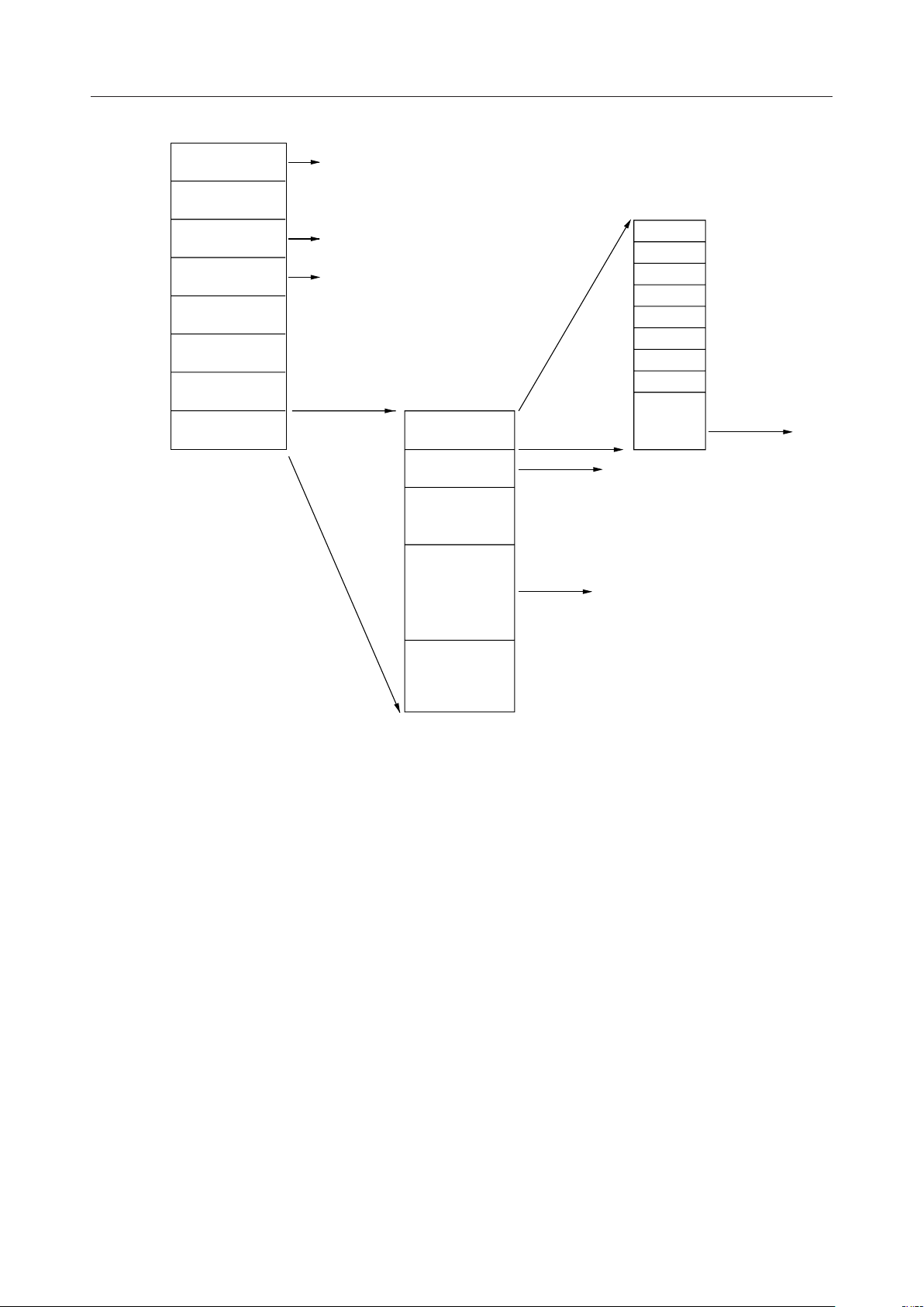
Register space is assigned to 0xE0000000-0xFFFFFFFF. Within this space, 0xF8000000-0xFFFFFFFF
is assigned for standard I/O and system registers.
46/95
Page 47
MSM7630¡ Semiconductor
0xF8000000
0xF8FFFFFF
0xF9000000
0xF9FFFFFF
0xFA000000
0xFAFFFFFF
0xFB000000
0xFBFFFFFF
0xFC000000
0xFCFFFFFF
0xFD000000
0xFDFFFFFF
0xFE000000
0xFEFFFFFF
0xFF000000
0xFFFFFFFF
TMR
SIO
PIO
0xFF000040
0xFF00005F
0xFF000080
BSR
SCR
System Registers
Test Circuit
BEA
ECR
0xFF000000
0xFF000004
0xFF000008
0xFF00000C
0xFF000010
0xFF000014
0xFF000018
0xFF00001C
0xFF000020
DRAMC
0xFF00003F
0xFF0000FF
47/95
Page 48
3. Registers
This is a register group used for bus control.
3.1 BEA: Bus Error Address
This register provides the address at the time a bus error occurred.
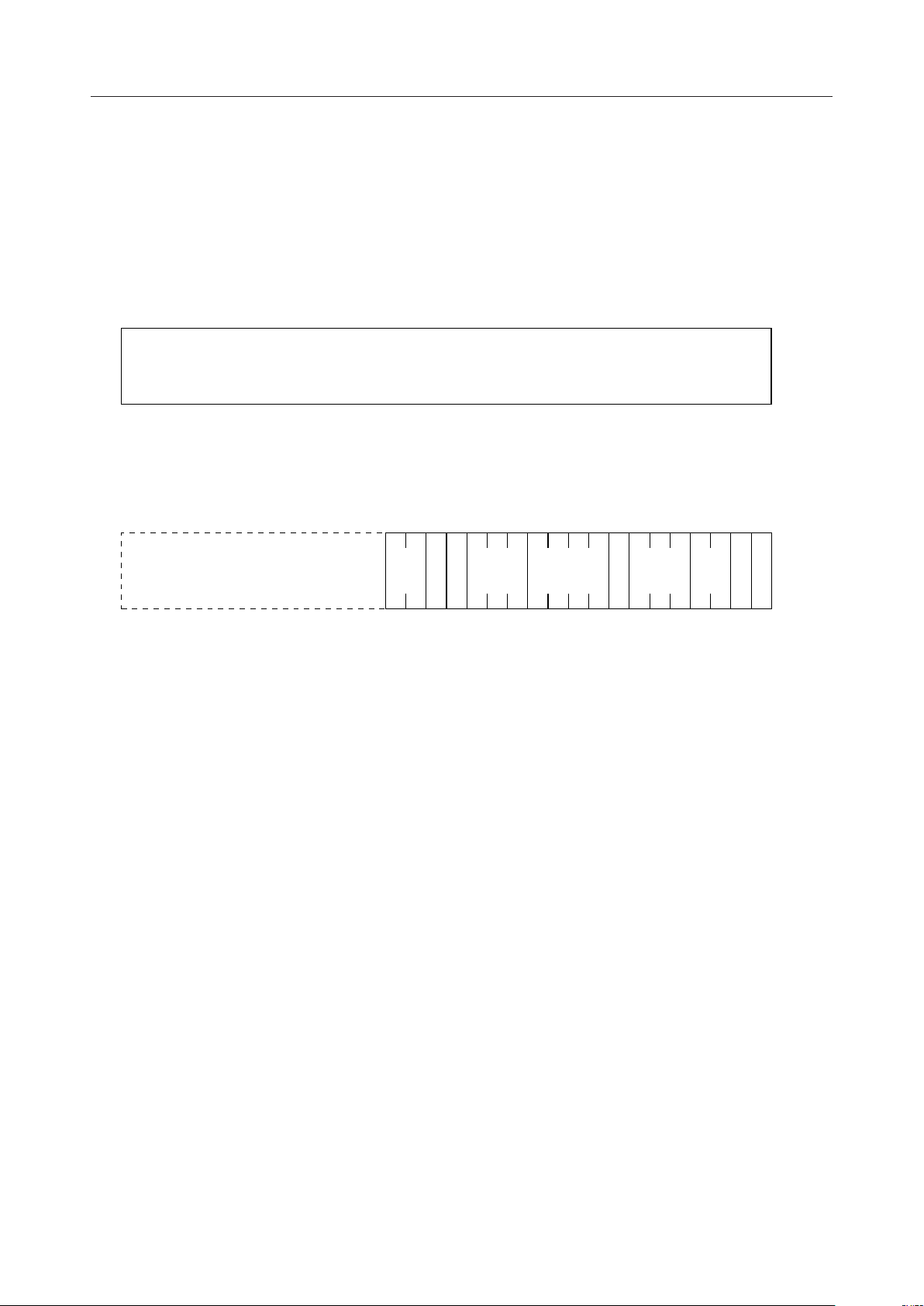
31 0bit
BEA
3.2 BSR: Bus Status Register
This register provides bus status information.
MSM7630¡ Semiconductor
31 19 18 17 16
bit 12
XSP
15 14 12
C
0ST
S
P
11 8
PEB
7 6 4
0 BES
30
0
0RH
• bit[18:17] XSP: Sleep (read/write)
When the STBY signal is "L", these bits either stop the clock without CPU intervention (XSP = 00)
or stop the clock after waiting for the CPU suspend process (XSP = 11).
• bit[16] CSP: CPU Sleep (read/write)
This bit indicates whether the CPU core is operating or suspended. Writing "1" will stop the CPU
core’s clock.
• bit[14:12] ST: Status (read-only)
These bits save the status signals when an access by the CPU core causes a bus error.
• bit[11:8] PEB: Parity Error Byte (read-only)
These bits provide the byte position when a parity error occurs.
• bit[6:4] BES: Bus Error Status (read-only)
These bits provide the source of a bus error.
BES = 000 No error
BES = 001 BIU register privilege violation
BES = 010 Parity error
BES = 100 Invalid space access
These bits will be "000" after reset.
48/95
Page 49
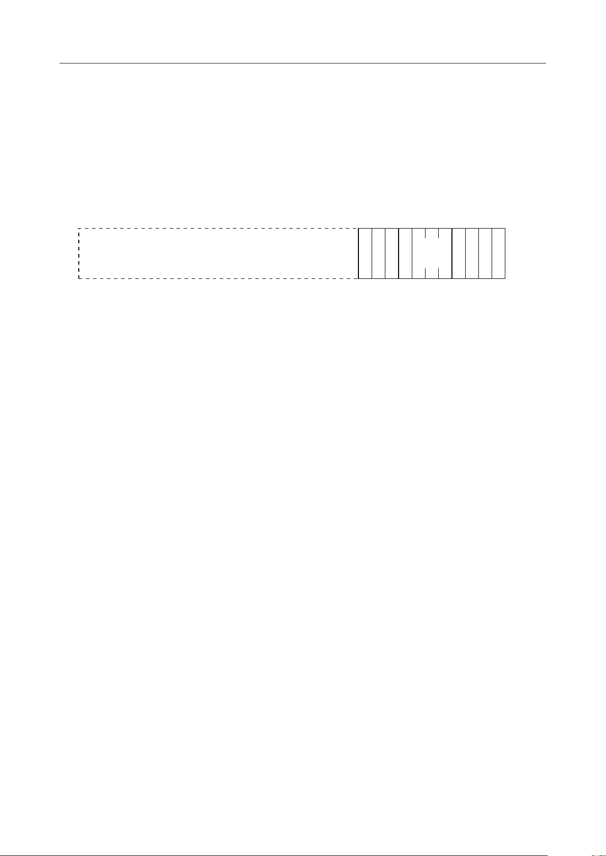
MSM7630¡ Semiconductor
• bit[1] H: Hold (read/write)
This bit sets whether or not bus rights will be passed upon a CPU core bus rights request. This bit
will be "0" after reset.
3.3 ECR: Extra Configuration Register
This register sets bus operation.
31 11 876 4
10 9
X
P
AXO
0
M
BM
• bit[10] OX: Internal ROM (read-only)
This bit indicates whether or not internal ROM will be accessed in 2 clocks.
MSM7630 does not use this bit.
• bit[9] AX: Internal RAM (read-only)
This bit indicates whether or not internal RAM will be accessed in 2 clocks.
MSM7630 does not use this bit.
• bit[7] PM: Parity Mode (read/write)
This bit sets parity.
PM = 0 Even parity
PM = 1 Odd parity
30bit
12
AVOVD
A
V
This bit will be "0" after reset.
MSM7630 does not use parity checking, so it ignores this field.
• bit[3] A: All Internal ROM (read/write)
This bit sets whether or not internal ROM will be accessed instead of external ROM.
MSM7630 has no internal ROM, so this bit is always "0".
• bit[2] OV: Internal ROM Valid (read-only)
This bit shows whether internal ROM is enabled or disabled.
This bit is "0" for MSM7630.
• bit[1] AV: Internal RAM Valid (read-only)
This bit shows whether internal RAM is enabled or disabled.
This bit is "0" for MSM7630.
49/95
Page 50

3.4 SCR: Space Configuration Register
This register sets ROM space, SRAM space, and general device space.
MSM7630¡ Semiconductor
31 18 17 16AS15 14 12 10 8OS76 4
A
A
C
D
202123242526 13 9 5
ODO
AWWARW
0
C
ORW
D
S
C
SDP
30bit 12
X
WT SZ
• bit[25] AC: SRAM Parity Check (read/write)
This bit sets parity checking of SRAM space. It will be "0" after reset.
AC = 0 Ignore parity checks.
AC = 1 Generate a bus error if a parity error is detected.
• bit[24] AD: SRAM Dummy Cycle (read/write)
This bit sets whether or not SRAM space may be accessed continuously after ROM space or DRAM
space has been read.
AD = 0 Continuous access allowed.
AD = 1 Open an interval of at least one clock.
This bit will be "1" after reset.
• bit[23:21] ARW: SRAM Read Wait (read/write)
These bits set the wait count when SRAM space is accessed by a read.
ARW = 000 2t access (1 wait)
ARW = 001 3t access (2 waits)
ARW = 010 4t access (3 waits)
ARW = 011 5t access (4 waits)
ARW = 100 6t access (5 waits)
ARW = 101 8t access (7 waits)
ARW = 110 10t access (9 waits)
ARW = 111 12t access (11 waits)
These bits will be "111" after reset.
50/95
Page 51

• bit[20:18] AWW: SRAM Write Wait (read/write)
These bits set the wait count when SRAM space is accessed by a write.
AWW = 000 2t access (1 wait)
AWW = 001 3t access (2 waits)
AWW = 010 4t access (3 waits)
AWW = 011 5t access (4 waits)
AWW = 100 6t access (5 waits)
AWW = 101 8t access (7 waits)
AWW = 110 10t access (9 waits)
AWW = 111 12t access (11 waits)
These bits will be "111" after reset.
• bit[17:16] AS: SRAM Device Size (read/write)
These bits set the device size of SRAM space.
MSM7630¡ Semiconductor
AS = 00 No SRAM (space is invalid)
AS = 01 8-bit wide device
AS = 10 16-bit wide device
AS = 11 32-bit wide device
These bits will be "00" after reset. When this field is "00", attempting to access SRAM space will
cause an instruction access exception or data access exception.
• bit[14] OC: ROM Parity Check (read/write)
This bit sets parity checking for ROM space. It will be "0" after reset.
OC = 0 Ignore parity errors.
OC = 1 Generate a bus error if a parity error is detected.
This bit will be "0" for the MSM7630.
• bit[13] OD: ROM Dummy Cycle (read/write)
This bit sets whether or not a ROM space access will immediately follow an SRAM space or DRAM
space read.
OD = 0 Consecutive access enabled.
OD = 1 Force an interval of at least one clock.
This bit will be "1" after reset.
51/95
Page 52

• bit[12:10] ORW: ROM Read Wait (read/write)
These bits set the wait count when ROM space is accessed by a read.
ORW = 000 2t access (1 wait)
ORW = 001 3t access (2 waits)
ORW = 010 4t access (3 waits)
ORW = 011 5t access (4 waits)
ORW = 100 6t access (5 waits)
ORW = 101 8t access (7 waits)
ORW = 110 10t access (9 waits)
ORW = 111 12t access (11 waits)
These bits will be "111" after reset.
• bit[9:8] OS: ROM Device Size (read/write)
These bits set the device size of ROM space.
MSM7630¡ Semiconductor
OS = 00 No ROM (space is invalid)
OS = 01 8-bit wide device
OS = 10 16-bit wide device
OS = 11 32-bit wide device
When this field is "00", attempting to access ROM space will cause an instruction access exception
or data access exception.
• bit[7] DS: Other Data Setup (read/write)
This bit sets whether or not the data setup time to the write strobe signal WR is guaranteed during
writes to general device space.
DS = 0 Not guaranteed.
DS = 1 Guaranteed.
This bit will be "1" after reset.
• bit[6] PC: Other Parity Check (read/ write)
This bit sets parity checking for general device space. It will be "0" after reset.
PC = 0 Ignore parity errors.
PC = 1 Generate a bus error if a parity error is detected.
This bit will be "0" for the MSM7630.
52/95
Page 53

MSM7630¡ Semiconductor
• bit[5] SD: Other Dummy Cycle (read/write)
This bit sets whether or not a general device space access will immediately follow an SRAM space
or DRAM space read.
SD = 0 Consecutive access enabled.
SD = 1 Force an interval of at least one clock.
This bit will be "1" after reset.
• bit[4] X: External Bus Clock Unit (read/write)
This bit sets the operating clock unit for general device space.
X = 0 Use 1 clock as the unit.
X = 1 Use 2 clocks as the unit.
This bit will be "0" after reset.
• bit[3:2] WT: Other Wait (read/write)
These bits set the wait count when general device space is accessed.
WT = 00 4t access
WT = 01 5t access
WT = 10 6t access
WT = 11 7t access
These bits will be "11" after reset.
• bit[1:0] SZ: Other Device Size (read/write)
These bits set the device size of general device space.
SZ = 00 No general device (space is invalid)
SZ = 01 8-bit wide device
SZ = 10 16-bit wide device
SZ = 11 32-bit wide device
These bits will be "11" after reset. When this field is "00", attempting to access general device space
will cause an instruction access exception or data access exception.
53/95
Page 54

3.5 DRAM: DRAM Configuration Register
This register sets DRAM space.
MSM7630¡ Semiconductor
31 28 27 26 25 24TP23 22 21 20 18 17 16
bit
0
29
00 DT
M
E
D
MD CA
P
RA CS
15 13 12 11 10 9
SZRF
M
0
RFC
After this register has been written, DRAM must not be accessed until the DRAM is operating
properly. Refer to the data sheet of the DRAM used to obtain the required conditions for proper
DRAM operation.
• bit[28:27] DT: Device Type (read/write)
These bits set the DRAM device type.
DT = 00 Fast page mode
DT = 01 Hyperpage mode (EDO DRAM)
These bits will be "00" after reset.
• bit[26] PR: Parity Check (read/write)
This bit sets parity checking for DRAM space. It will be "0" after reset.
PR = 0 Ignore parity errors.
PR = 1 Generate a bus error if a parity error is detected.
This bit will be "0" for the MSM7630.
• bit[25:24] TP: Type (read/write)
This bit sets the DRAM’s RAS signal and byte position control signal.
TP = 00 1 RAS mode, byte position CAS control
TP = 01 2 RAS mode, byte position CAS control
TP = 10 1 RAS mode, byte position WE control
TP = 11 2 RAS mode, byte position WE control
These bits will be "00" after reset.
• bit[23] DP: Data Priority (read/write)
This bit sets the priority of processing when data access is requested by a load/store instruction
during a one-line instruction cache read from DRAM due to an instruction cache miss.
DP = 0 Give priority to the instruction cache read from DRAM.
DP = 1 Give priority to the data access.
This bit will be "0" after reset.
54/95
Page 55

• bit[22:21] MD: Mode (read/write)
These bits set the number of clocks for a DRAM access.
MD = 01 2n clock access
MD = 10 3n clock access
These bits will be "10" after reset.
• bit[20:18] RA: Row Address (read/write)
These bits set the most significant bit position of the row address.
RA = 000 A17
RA = 001 A18
RA = 010 A19
RA = 011 A20
RA = 100 A21
RA = 101 A22
RA = 110 A23
MSM7630¡ Semiconductor
These bits will be "000" after reset.
• bit[17:16] RS: Row Shift (read/write)
These bits set how many bits to shift the row address to output it as a DRAM address.
RS = 00 8-bit shift
RS = 01 9-bit shift
RS = 10 10-bit shift
RS = 11 11-bit shift
These bits will be "00" after reset.
• bit[15:13] CA: Column Address (read/write)
These bits set the most significant bit position of the column address.
CA = 000 A08
CA = 001 A09
CA = 010 A10
CA = 011 A11
CA = 100 A12
These bits will be "000" after reset.
55/95
Page 56

MSM7630¡ Semiconductor
• bit[12:11] SZ: Device Size (read/write)
These bits set the device size of DRAM space.
SZ = 00 No DRAM (space is invalid)
SZ = 01 8-bit wide device
SZ = 10 16-bit wide device
SZ = 11 32-bit wide device
These bits will be "00" after reset. When this field is "00", attempting to access DRAM space will
cause an instruction access exception or data access exception.
• bit[10] RFM: Refresh Mode (read/write)
This bit sets the refresh operation mode.
RFM = 0 CAS-before-RAS refresh
RFM = 1 CAS-before-RAS self-refresh
This bit will be "0" after reset.
• bit[9:0] RFC: Refresh Counter (read/write)
These bits set the initial value of the refresh counter. It should be set as an integer value obtained
by:
[(refresh period) ÷ (clock period) ÷ 16] – 1
These bits will be "0000000000" after reset.
56/95
Page 57
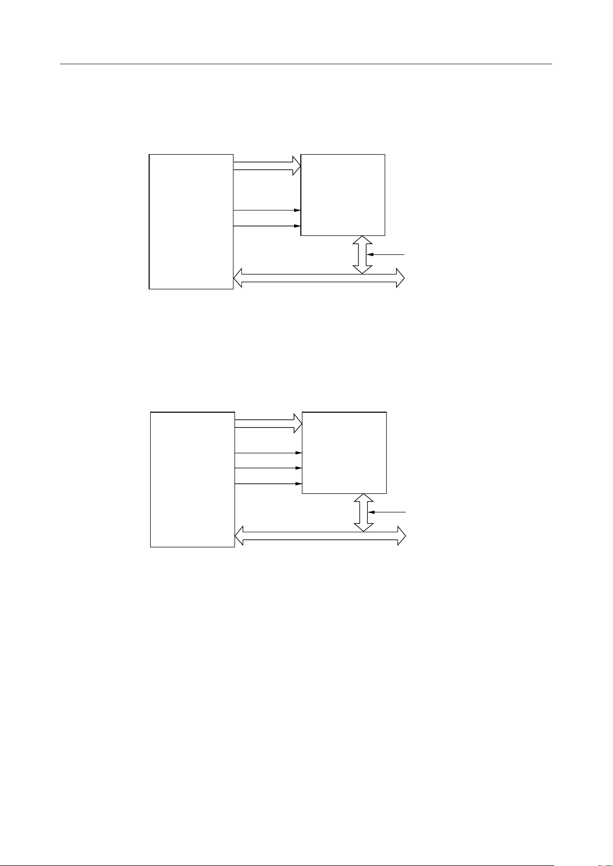
4. ROM Access
The MSM7630 interface with ROM is shown below.
MSM7630¡ Semiconductor
Axx
ROM
RD
MSM7630
Axx
CS
OE
ROM
Dxx
Data
External Bus
The ROM signal will become "0" when the address signal and specified ROM space match. Refer to
the timing diagram for basic timing of ROM accesses.
5. SRAM Access
The MSM7630 interface with SRAM is shown below.
Axx
SRAM CS
WE
RD
Axx
WE
OE
SRAM
Dxx
Data
MSM7630
External Bus
The SRAM signal will become "0" when the address signal and specified SRAM space match. Refer
to the timing diagram for basic timing of SRAM accesses.
57/95
Page 58
MSM7630¡ Semiconductor
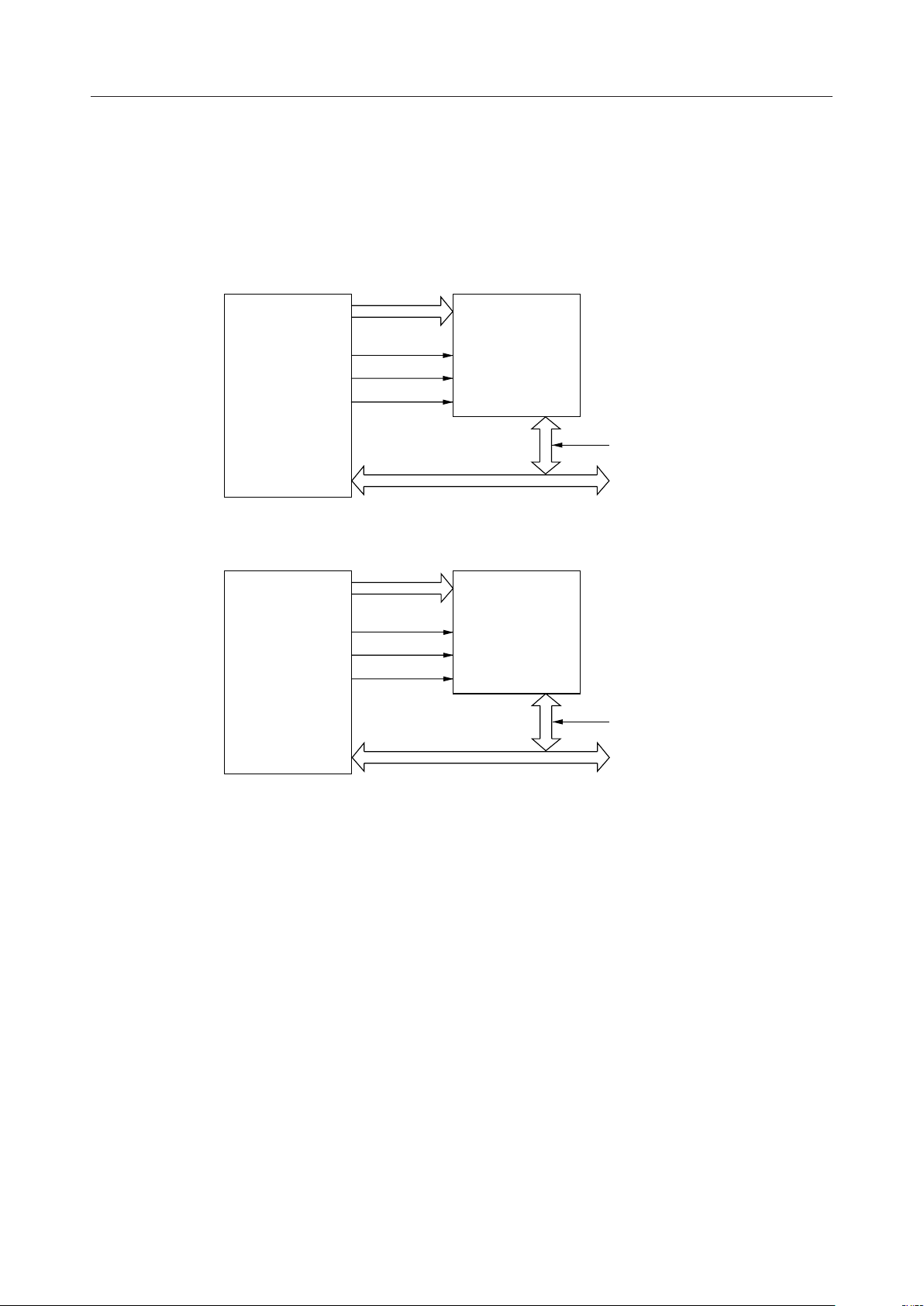
6. DRAM Access
There are two MSM7630 interfaces with DRAM: one when byte position is specified by CAS, and one
when byte position is specified by WE. This is set by the DRAM register’s TP field.
An interface example when byte position is specified by CAS is shown below.
Axx
RAS RAS
CAS [0 : 1]
WE
MSM7630
Axx
CAS
WE
DRAM
Dxx
Data
External Bus
An interface example when byte position is specified by WE is shown below.
Axx
RAS RAS
WE
CAS [0 : 1]
MSM7630
Axx
CAS
WE
DRAM
Dxx
Data
External Bus
Refer to the timing chart for basic timing of DRAM accesses.
58/95
Page 59

MSM7630¡ Semiconductor
The table below shows how address signals are connected for different DRAM configurations.
Configuration Row Column Address lines CA RS RA
256K ¥ 8
256K ¥ 16
256K ¥ 32
512K ¥ 8
512K ¥ 16
512K ¥ 32
1M ¥ 8
1M ¥ 16
1M ¥ 32
2M ¥ 8
2M ¥ 16
2M ¥ 32
4M ¥ 8
4M ¥ 16
4M ¥ 32
17-09 08-00 A[08:00] 000 01 000
18-10 09-01 A[09:01] 001 01 001
18-09 08-01 A[09:01] 000 00 001
19-11 10-02 A[10:02] 010 01 010
19-10 09-02 A[11:02] 001 00 010
18-09 08-00 A[09:00] 000 01 001
19-10 09-01 A[10:01] 001 01 010
20-11 10-02 A[11:02] 010 01 011
19-10 09-00 A[09:00] 001 10 010
20-11 10-01 A[10:01] 010 10 011
20-10 09-01 A[11:01] 001 01 011
20-09 08-01 A[12:01] 000 00 011
21-12 11-02 A[11:02] 011 10 100
21-11 10-02 A[12:02] 010 01 100
21-10 09-02 A[13:02] 001 00 100
20-10 09-00 A[10:00] 001 10 011
20-09 08-00 A[11:00] 000 01 011
21-11 10-01 A[11:01] 010 10 100
21-10 09-01 A[12:01] 001 01 100
22-12 11-02 A[12:02] 011 10 101
22-11 10-02 A[13:02] 010 01 101
21-11 10-00 A[10:00] 010 11 100
21-10 09-00 A[11:00] 001 10 100
22-12 11-01 A[11:01] 011 11 101
22-11 10-01 A[12:01] 010 10 101
23-13 12-02 A[12:02] 100 11 110
23-12 11-02 A[13:02] 011 10 110
59/95
Page 60

MSM7630¡ Semiconductor
Serial Interface
1. Features
The serial interface (SIO) performs both clock synchronized and start-stop transfers.
2. SIO Functions
2.1 Port Configuration
• Independent transmit and receive circuits
• Double buffer configuration for receive buffer
Because the transmit and receive circuits are independent, start-stop transfers are all full-duplex
communication.
2.2 Transfer Methods
• Start-stop transfer
Data length: 7 bits or 8 bits selectable
Transfer sequence: LSB first
Stop bits: 1 bit or 2 bits selectable
Parity bit: No parity, even parity, or odd parity selectable
Flag bit: Enables inter-processor communication using the serial port.
• Clock synchronized transfer
Data length: 8 bits fixed
Transfer sequence: LSB first
However, cannot be used together with parity bit.
60/95
Page 61
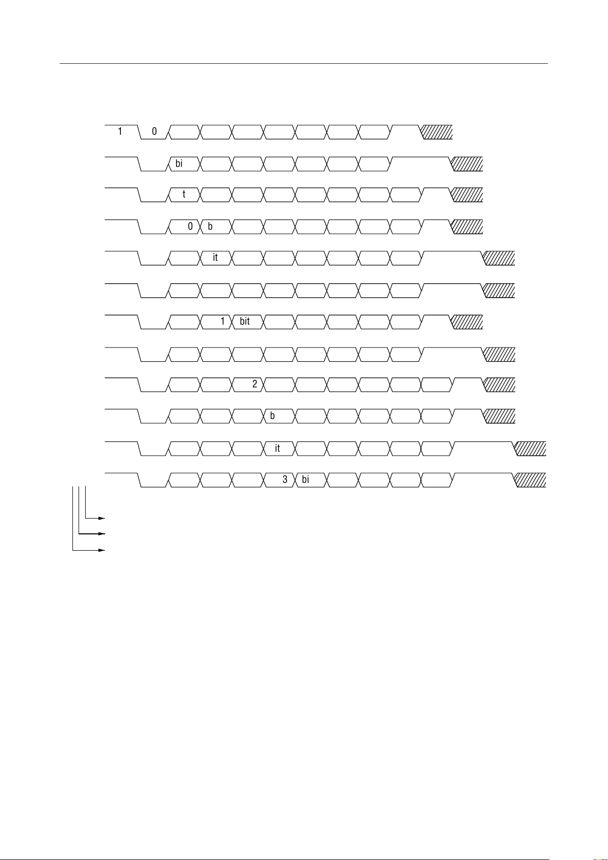
The chart below shows the data format with start-stop transfers.
(*)
MSM7630¡ Semiconductor
7N1
7N2
7F1
7P1
7F2
7P2
8N1(*)
8N2
8F1
8P1
1 0 bit 0 bit 1 bit 2 bit 3 bit 4 bit 5 bit 6 1
1 0 bit 0 bit 1 bit 2 bit 3 bit 4 bit 5 bit 6 1 1
1 0 bit 0 bit 1 bit 2 bit 3 bit 4 bit 5 bit 6 Flag 1
1 0 bit 0 bit 1 bit 2 bit 3 bit 4 bit 5 bit 6 Parity 1
1 0 bit 0 bit 1 bit 2 bit 3 bit 4 bit 5 bit 6 Flag 1 1
1 0 bit 0 bit 1 bit 2 bit 3 bit 4 bit 5 bit 6 Parity 1 1
1 0 bit 0 bit 1 bit 2 bit 3 bit 4 bit 5 bit 6 bit 7 1
1 0 bit 0 bit 1 bit 2 bit 3 bit 4 bit 5 bit 6 bit 7 1 1
1 0 bit 0 bit 1 bit 2 bit 3 bit 4 bit 5 bit 6 bit 7 1Flag
1 0 bit 0 bit 1 bit 2 bit 3 bit 4 bit 5 bit 6 bit 7 1Parity
8F2
8P2
1 0 bit 0 bit 1 bit 2 bit 3 bit 4 bit 5 bit 6 bit 7 1Flag
1 0 bit 0 bit 1 bit 2 bit 3 bit 4 bit 5 bit 6 bit 7 1Parity
Stop bits
Flag/parity
Data size 7 : 7 bits, 8 : 8 bits
After reset the format will be 8 bits, no parity, 1 stop bit.
1 : 1 Stop Bit, 2 : 2 Stop Bits
N : Non, F : Flag, P : Parity
1
1
61/95
Page 62

2.3 Baud Rate
• Internal baud rate generator
• Clock synchronized transfers
B = f/(8 ¥ n ¥ (256 – P))
where
B : baud rate (bps)
f : processor (SCP) clock frequency (Hz)
n : baud rate parameter
One of 1, 2, 4, 8, 16, 32, and 64. Selected by SBR’s SBRP field.
(Refer to the register description.)
P : baud rate adjustment value (0 £ P £ 255)
Set by SBR’s SBRV field. (Refer to the register description.)
MSM7630¡ Semiconductor
At a processor (SCP) clock of 20 MHz, the maximum transfer rate is 2.5 Mbps. At 40 MHz, the
maximum transfer rate is 5 Mbps.
• Start-stop transfers
B = f/(16 ¥ n ¥ (256 – SBR))
where
B : baud rate (bps)
f : processor (SCP) clock frequency (Hz)
n : baud rate parameter
One of 1, 2, 4, 8, 16, 32, and 64. Selected by SBR’s SBRP field.
(Refer to the register description.)
SBR : baud rate adjustment value (0 £ SBR £ 255)
Set by SBR’s SBRV field. (Refer to the register description.)
2.4 Error Detection
• Parity errors (start-stop transfers)
A parity error will be detected when a parity bit generated from received data does not match the
received parity bit.
• Framing errors (start-stop transfers)
A framing error will be detected when a received stop bit is "0". When 2 stop bits have been selected,
only the first bit received will be checked.
• Overrun errors (start-stop and clock synchronized transfers)
An overrun error will be detected when the next receive frame's stop bit is detected before the
receive buffer has been read.
62/95
Page 63

MSM7630¡ Semiconductor
2.5 Interrupts
The SIO is the source of the following interrupts.
• Interrupts
- Receive error interrupt
A receive error interrupt will be generated whenever a parity error, framing error, or overrun
error is detected.
- Receive buffer full interrupt
A receive buffer full interrupt will be generated whenever the valid receive data has been
transferred to the receive buffer.
- Transmit buffer empty interrupt
A transmit buffer empty interrupt will be generated whenever the transmit buffer becomes
empty.
- Transmit end interrupt
A transmit end interrupt will be generated whenever an SIO data transfer ends.
- Modem status interrupt
A modem status interrupt will be generated whenever a change in a modem control input signal
(CTS, DSR) is detected.
• Interrupt enable/disable
Each interrupt source can be independently enabled or disabled. Also, all interrupts can be
disabled at once.
• Interrupt requests
Whenever any of the five interrupts above is enabled and its conditions are fulfilled, the CPU will
get an SIO interrupt request.
63/95
Page 64

3. SIO Registers
These registers control SIO.
3.1 SIB: SIO Input Buffer
This register holds data that has been input externally. It is undefined after reset.
MSM7630¡ Semiconductor
7bit
SIB
0
3.2 SOB: SIO Output Buffer
This register holds data to be output externally. It is undefined after reset.
7bit
SOB
0
3.3 SSTS: SIO Status Register
This register provides SIO status.
15 11
S
S
S
M
S
O
I
S
S
S
I
T
T
S
S
P
O
F
00000
V
E
0
T
R
E
E
12345678910
0bit
S
S
S
S
E
R
T
T
R
X
X
E
I
I
I
I
• bit[10] SOVE
0 : No overrun error
1 : Overrun error generated
This bit can only be written with "0". It will be "0" after reset.
• bit[9] SFRE
0 : No framing error
1 : Framing error generated
This bit can only be written with "0". It will be "0" after reset.
64/95
Page 65

• bit[8] SPTE
0 : No parity error
1 : Parity error generated
This bit can only be written with "0". It will be "0" after reset.
• bit[6] SMSI
0 : No modem status interrupt
1 : Modem status interrupt requested
This bit is read-only. It will be "0" after reset.
• bit[5] SOST
0 : Transmit buffer full
1 : Transmit buffer empty
MSM7630¡ Semiconductor
This bit can only be written with "0". It will be "1" after reset.
• bit[4] SIST
0 : Receive buffer empty
1 : Receive buffer full
This bit can only be written with "0". It will be "0" after reset.
• bit[3] SERI
0 : No receive error interrupt
1 : Receive error interrupt requested
This bit is read-only. It will be "0" after reset.
• bit[2] SRXI
0 : No receive buffer full interrupt
1 : Receive buffer full interrupt requested
This bit is read-only. It will be "0" after reset.
• bit[1] STXI
0 : No transmit buffer empty interrupt
1 : Transmit buffer empty interrupt requested
This bit is read-only. It will be "0" after reset.
65/95
Page 66

• bit[0] STEI
0 : No transmit end interrupt
1 : Transmit end interrupt requested
This bit can only be written with "0". It will be "0" after reset.
3.4 SCMD: SIO Command Register
MSM7630¡ Semiconductor
15 11
S
R
E
N
121314
S
S
S
S
T
0
E
N
R
T
E
I
X
X
R
E
I
I
I
N
E
E
E
S
S
S
T
M
E
0
O
I
D
E
• bit[15] SREN
0 : Data receive disabled
1 : Data receive enabled
This bit will be "0" after reset.
• bit[14] STEN
0 : Data transmit disabled
1 : Data transmit enabled
This bit will be "0" after reset.
• bit[12] SIEN
M
0bit
12345678910
S
S
S
F
F
F
B
B
L
S
S
P
S
T
T
Y
P
0 : Interrupts disabled
1 : Interrupts enabled
This bit will be "0" after reset.
• bit[11] SERIE
0 : Receive error interrupts disabled
1 : Receive error interrupts enabled
This bit will be "0" after reset.
• bit[10] SRXIE
0 : Receive buffer full interrupts disabled
1 : Receive buffer full interrupts enabled
This bit will be "0" after reset.
66/95
Page 67

• bit[9] STXIE
0 : Transmit buffer empty interrupts disabled
1 : Transmit buffer empty interrupts enabled
This bit will be "0" after reset.
• bit[8] STEIE
0 : Transmit end interrupts disabled
1 : Transmit end interrupts enabled
This bit will be "0" after reset.
• bit[6] SMOD
0 : Start-stop transfer mode
1 : Clock synchronized transfer mode
MSM7630¡ Semiconductor
This bit will be "0" after reset.
• bit[5] SFBM
0 : Clear flag bit mode
1 : Set flag bit mode
This bit will be "0" after reset.
• bit[4] SFB
0 : Flag bit value set to "0"
1 : Flag bit value set to "1"
This bit will be "0" after reset.
• bit[3] SFL
0 : Transfer data length is 8 bits
1 : Transfer data length is 7 bits
This bit will be "0" after reset.
• bit[2:1] SPTY
00 : No parity
10 : Even parity
11 : Odd parity
These bits will be "00" after reset.
67/95
Page 68
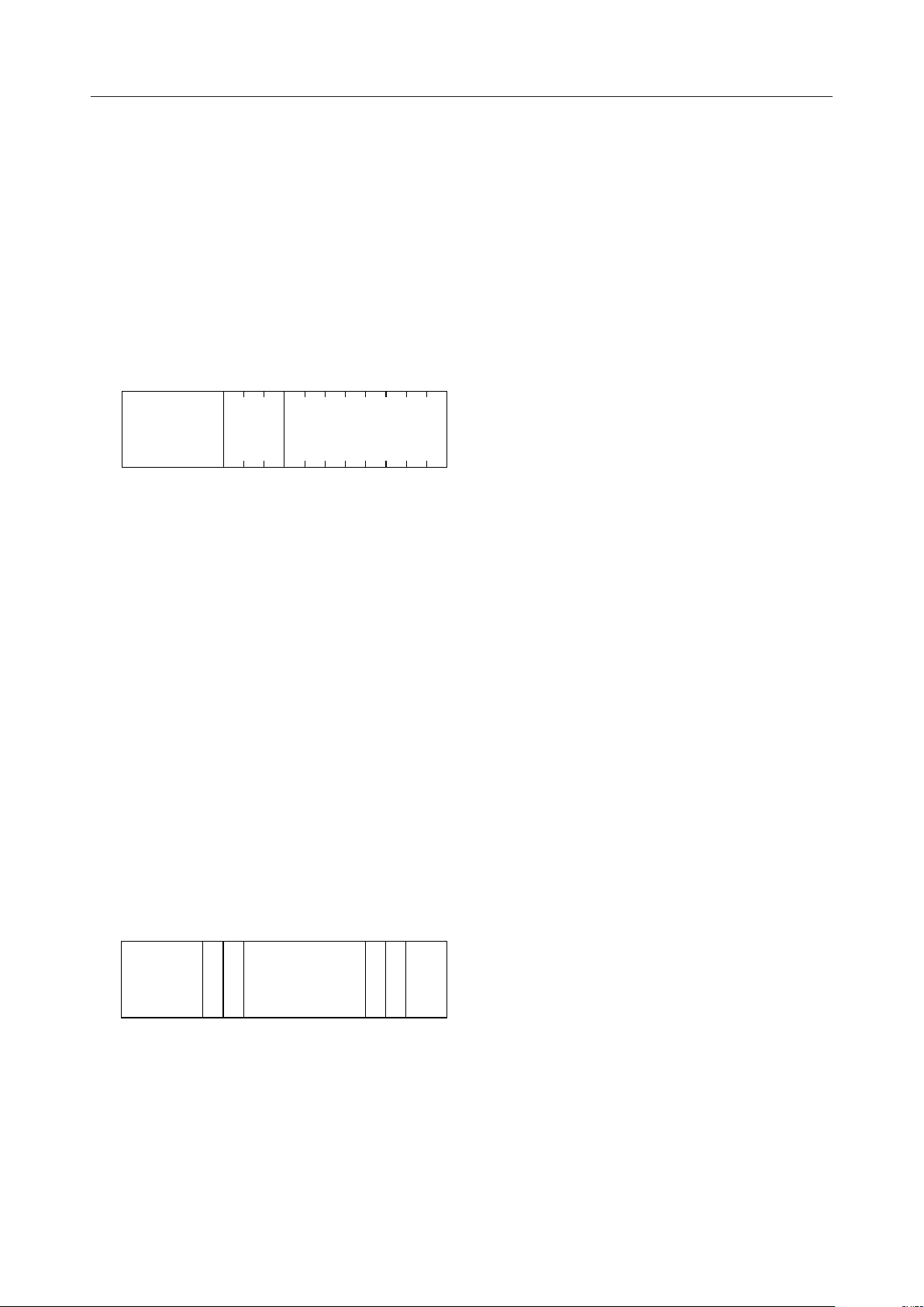
• bit[0] SSTP
0 : 1 stop bit
1 : 2 stop bits
This bit will be "0" after reset.
3.5 SBR: Baud Rate Adjustment Register
This register sets values that adjust the baud rate.
MSM7630¡ Semiconductor
15 11 0bit
0
0000SBRP SBRV
7810
• bit[10:8] SBRP
000 : Baud rate parameter n = 1
001 : Baud rate parameter n = 2
010 : Baud rate parameter n = 4
011 : Baud rate parameter n = 8
100 : Baud rate parameter n = 16
101 : Baud rate parameter n = 32
110 : Baud rate parameter n = 64
These bits will be undefined after reset.
• bit[7:0] SBRV
These bits are the baud rate adjustment value. They will be undefined after reset.
3.6 MSTS: Modem Status Register
This register provides the states of modem signals.
15 11 0bit
12
0
000
D
D
D
C
T
S
00 000
S
R
0
1234910
C
D
00
T
S
S
R
• bit[11] DCTS
0 : CTS signal has not changed
1 : CTS signal has changed
This bit is read-only. It will be "0" after reset.
68/95
Page 69
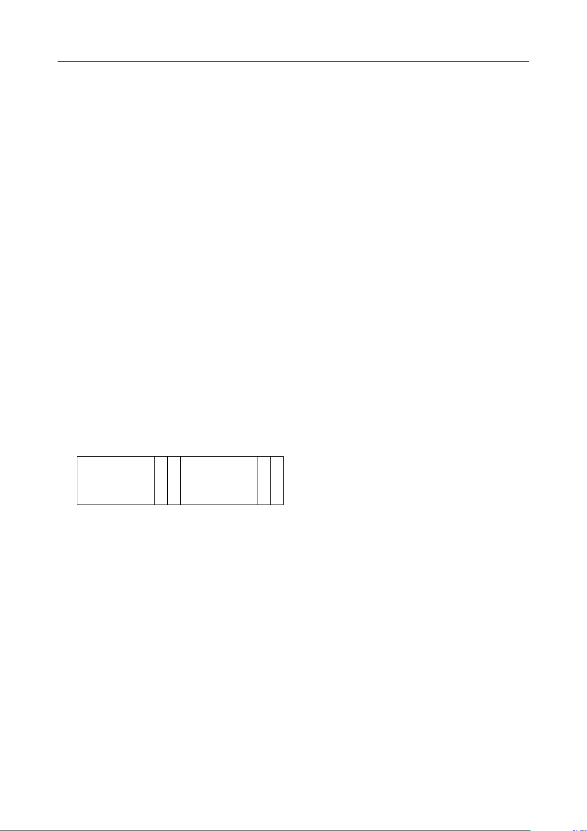
• bit[10] DDSR
0 : DSR signal has not changed
1 : DSR signal has changed
This bit is read-only. It will be "0" after reset.
• bit[3] CTS
0 : CTS input signal value = "0"
1 : CTS input signal value = "1"
This bit is read-only. It will be the CTS pin input value after reset.
• bit[2] DSR
0 : DSR input signal value = "0"
1 : DSR input signal value = "1"
MSM7630¡ Semiconductor
This bit is read-only. It will be the DSR pin input value after reset.
3.7 MCMD: Modem Command Register
This register enables/disables modem status interrupts and auto-enable mode, and controls RTS
and DTR output signals.
15 0bit
0
000
87
D
D
C
D
0
00 00
T
S
S
R
000
12910
C
D
T
S
S
R
• bit[9] SMSIE
0 : Disables modem status interrupts
1 : Enables modem status interrupts
This bit will be "0" after reset.
• bit[8] SAEN
0 : Disables auto-enable mode
1 : Enables auto-enable mode
This bit will be "0" after reset.
• bit[1] RTS
0 : Output RTS signal "0"
1 : Output RTS signal "1"
This bit will be "0" after reset.
69/95
Page 70

• bit[0] DTR
0 : Output DTR signal "0"
1 : Output DTR signal "1"
This bit will be "0" after reset.
3.8 SCNT: SIO Control Register
This register controls SIO.
15 0bit
0
00 0000 0
000 0 000
• bit[0] CSTP
MSM7630¡ Semiconductor
C
S
T
P
0 : Enable SIO clock supply
1 : Disable SIO clock supply
This bit will be "0" after reset.
70/95
Page 71

MSM7630¡ Semiconductor
4. SIO Register Addresses
SIO register addresses for the MSM7630 are shown below.
0xFA000000 SIO Input Buffer
0xFA000004 SIO Output Buffer
0xFA000008 Baud Rate Adjustment Register
0xFA00000C SIO Status Register
0xFA000010 SIO Command Register
0xFA000014 Modem Status Register
0xFA000018 Modem Command Register
0xFA00001C SIO Control Register
5. SIO Operation
There are two methods of SIO operation: start-stop transfers where communication is performed
synchronized to characters, and clock synchronized transfers where communication is performed
synchronized to the clock.
5.1 Clock Synchronized Transfers
Clock synchronized transfer mode is selected by setting the SCMD (Command Register) SMOD bit
to "1". In this mode 8-bit data will be input/output synchronized to the clock output from the SCLK
pin.
With clock synchronized transfers, transfer data is only 8 bits, so parity bits and flag bits cannot be
added. The SCMD (Command Register) SFBM bit, SFL bit, and SPTY bits will be set to "0", "0", and
"00" respectively.
5.1.1 Clock Synchronized Transfer Baud Rate
f
B =
8 ¥ n ¥ (256 – P)
where
B : baud rate
f : SCP clock frequency
n : baud rate parameter (set by SBR register’s SBRP bit)
P : baud rate adjustment value (set by SBR register’s SBRV bit)
Set SBR (Baud Rate Adjustment Register) to achieve the required baud rate.
71/95
Page 72

MSM7630¡ Semiconductor
5.1.2 Clock Synchronized Transmit Operation
1) Verify that the SSTS (Status Register) SOST bit is "1", and then write the data to be transferred to
the transmit buffer SOB.
2) Write "0" to SOST to indicate that SOB has valid data.
3) If using SIO interrupts, set the SCMD (Command Register) SIEN bit to "1". If using the transmit
buffer empty interrupt, write "1" to the SCMD STXIE bit. If using the transmit end interrupt, write
"1" to the SCMD STEIE bit.
4) If the MCMD (Modem Command Register) SAEN bit is "0", then setting the SCMD (Command
Register) STEN bit to "1" will start the transfer. If the MCMD SAEN bit is "1", then the transfer will
start when the SCMD STEN bit is "1" and the CTS input is "1".
5) SOB (Transmit Buffer) data will be transferred LSB first from the TXD output. Also, a synchronous
clock will be transmitted from the SCLK pin. Data on the TXD output will change synchronous
to the falling edge of SCLK. The receiving device should sample TXD data on the rising edge of
SCLK.
6) When the next data can be written to the transmit buffer, the SSTS (Status Register) SOST bit will
change from "0" to "1". If the SCMD (Command Register) STXIE and SIEN bits are "1" at this time,
then the SSTS STXI bit will become "1" and an interrupt request to the CPU will be generated.
7) For continuous transfers, after the SSTS (Status Register) SOST bit becomes "1" write new data to
SOB (Transmit Buffer) and write "0" to the SOST bit.
8) If there is no more data to be transmitted, then write "0" to the SCMD (Command Register) STXIE
bit. This will disable interrupt requests from SIO.
9) When transfer of the eighth bit of data ends, the SSTS (Status Register) SOST bit will become "1"
(transmit buffer SOB is empty), SCLK will stop, and the transmit operation will end. If the
SCMD’s STEIE and SIEN bits are "1" at this time, then the SSTS’s STEI bit will become "1" and an
interrupt request to the CPU will be generated. This interrupt can be released by writing "0" to the
SSTS’s STEI bit or the SCMD’s STEIE bit.
72/95
Page 73

MSM7630¡ Semiconductor
5.1.3 Clock Synchronized Receive Operation
1) The receive operation will begin if the MCMD’s SAEN bit is "0" (auto-enable mode disabled) and
the SCMD’s SREN bit is "1" (data receive enabled).
2) When the receive operation begins, a synchronous clock will be output from SCLK.
3) If using SIO interrupts, set SCMD’s SIEN bit to "1". If using the receive buffer full interrupt, set
SCMD’s SRXIE bit to "1".
4) The transmitting device should input the data to be transferred on RXD on the falling edge of
SCLK, LSB first. The SIO will sample RXD data on SCLK’s rising edge, shifting it into the Receive
Shift Register.
5) When the eighth bit of data has been received, the receive shift register’s data is transferred to SIB.
However, it will not be transferred to SIB if an overrun error occurs.
6) After data has transferred from the receive shift register to the receive buffer SIB, SIST will change
from "0" to "1", indicating that there is valid data in the receive buffer SIB. If SCMD’s SRXI bit and
SIEN bit are both "1" at this time, an interrupt request to the CPU will be generated.
7) To continue receiving data, read the SIB data after SIS becomes "1", and then write "0" to SIST.
8) To end the receive operation, write "0" to SCMD’s SREN bit. At the time "0" is written to SREN,
data currently being received will be transferred to SIB and the receive operation will end.
9) When SSTS’s SIST bit is "1" and the SIO enters the state in which data is ready to be transferred
from the receive shift register to the receive buffer, the SIO will assume that an overrun error
(receipt of further data before the value of the receive buffer SIB is read) has occurred. SSTS’s SOVE
bit will then be set to "1". In this case the receive shift register value will not be transferred to the
receive buffer SIB. If SCMD’s SERIE bit and SIEN bit are "1", then SSTS's SERI bit will be set to "1"
and an interrupt request to the CPU will be generated. To release the interrupt, write "0" to SSTS’s
SOVE bit or to SCMD’s SERIE or SIEN bit.
5.2 Start-Stop Transfers
Start-stop transfer mode is selected by setting the SCMD (Command Register) SMOD bit to "0". In
this mode data is output LSB first from TXD, and input LSB first from RXD.
5.2.1 Start-Stop Transfer Baud Rate
f
B =
16 ¥ n ¥ (256 – P)
where
B : baud rate
f : SCP clock frequency
n : baud rate parameter (set by SBR register’s SBRP bit)
P : baud rate adjustment value (set by SBR register’s SBRV bit)
Set SBR (Baud Rate Adjustment Register) to achieve the required baud rate.
73/95
Page 74

MSM7630¡ Semiconductor
5.2.2 Start-Stop Transmit Operation
1) Verify that the SSTS (Status Register) SOST bit is "1", and then write the data to be transferred to
the transmit buffer SOB. Next write "0" to SOST to indicate that SOB has valid data.
2) If the MCMD (Modem Command Register) SAEN bit is "0", then setting the SCMD (Command
Register) STEN bit to "1" will start the transfer. If the MCMD SAEN bit is "1", then the transfer will
start when the SCMD STEN bit is "1" and the CTS input is "1".
3) For start-stop transmit operation, a start bit "0" will be output from TXD. Then the data written
in SOB will be output LSB first. If SCMD’s SFL bit is "0", then 8 bits of data will be output. If the
SFL bit is "1", then 7 bits will be output.
4) When SCMD (Command Register) SFBM bit is "0", a parity bit will be output after the SOB data.
The parity will be even if the SPTY field is "10", and odd if the SPTY field is "11". If SCMD’s SFBM
bit is "1" and SPTY is "00", then the value set in SCMD’s SFB bit will be output after the SOB data.
If SCMD’s SFBM bit is "0" and the SPTY field is "0", then neither a parity bit nor flag bit will be
output after SOB data.
5) Finally, one stop bit will be output if the SCMD (Command Register) SSTP bit is "0", or two stop
bits will be output if the SSTP bit is "1". This will end the transfer of one frame of data.
6) When the next data can be written to the transmit buffer, the SSTS (Status Register) SOST bit will
change from "0" to "1". If the SCMD (Command Register) STXIE and SIEN bits are "1" at this time,
then the SSTS STXI bit will become "1" and an interrupt request to the CPU will be generated.
7) For continuous transfers, after the SSTS (Status Register) SOST bit becomes "1" write new data to
SOB (Transmit Buffer) and write "0" to the SOST bit. This will disable interrupt requests from SIO.
8) If there is no more data to be transmitted, then write "0" to the SCMD (Command Register) STXIE
bit. The will disable interrupt requests from SIO.
9) When transfer of the stop bit ends, the transmit operation will end if the SOST bit is "1". If the
SCMD's STEIE and SIEN bits are "1" at this time, then the SSTS's STEI bit will become "1" and an
interrupt request to the CPU will be generated. This interrupt can be released by writing "0" to
the SSTS's STEI bit or the SCMD's STEIE or SINT bit.
74/95
Page 75

MSM7630¡ Semiconductor
5.2.3 Start-Stop Receive Operation
1) The receive operation can begin if the MCMD’s SAEN bit is "0" and the SCMD’s SREN bit is "1".
2) If using SIO interrupts, set SCMD’s SIEN bit to "1". If using the receive buffer full interrupt, set
SCMD’s SRXIE bit to "1". If using the receive error interrupt, set SCMD’s SERIE bit to "1".
3) The SIO receive operation will start when a falling edge is detected on RXD. The first bit of data
is received as the start bit. If the received value is "1", then it will not be recognized as a start bit,
the receive operation will be suspended, and the device will wait for another RXD falling edge to
be detected. If the received value is "0", then data will continue to be received.
4) When the start bit is received, receive of data will start. If SCMD’s SFL bit is "0", then 8 bits of data
will be input serially into the receive shift register. If the SFL bit is "1", then 7 bits of data will be
input.
5) When SCMD (Command Register) SFBM bit is "0", a parity bit will be received after the data. The
parity will be even if the SPTY field is "10", and odd if the SPTY field is "11". If SCMD’s SFBM bit
is "1" and SPTY is "00", one flag bit will be received. If SCMD’s SFBM bit is "0" and the SPTY field
is "00", then neither a parity bit nor flag bit will be received.
6) Finally one stop bit will be received. Even if SCMD’s SSTP bit is "1", only the first stop bit will be
received.
7) When all bits have been received, the data input in the receive shift register will be transferred to
the receive buffer SIB. However, if either of the following two conditions applies, then data will
not be transferred to SIB, and SIB will retain its previous value.
1. SCMD’s SFBM bit is "1", its SPTY field is "00", and the received flag bit does not match SCMD’s
SFB bit.
2. An overrun error occurred.
8) When data has been transferred from the receive shift register to the receive buffer SIB, SSTS’s SIST
will change from "0" to "1". If SCMD’s SRXIE and SIEN bits are both "1", then SSTS’s SRXI bit will
become "1" and an interrupt request to the CPU will be generated. To release the interrupt, write
"0" to SSTS’s SIST bit or to SCMD’s SRXIE or SIEN bit.
9) When SSTS’s SIST bit is "1" and the SIO enters the state in which data is ready to be transferred
from the receive shift register to the receive buffer, the SIO will assume that an overrun error
(receipt of further data before the value of the receive buffer is read) has occurred. SSTS’s SOVE
bit will then be set to "1".
10) If the received stop bit is "0", then it will be considered indication of a framing error. SSTS’s SFRE
bit will then be set to "1".
11) When SCMD’s SPTY field is "10" or "11", a mismatch between parity generated from the receive
data and the parity bit will be considered a parity error. SSTS’s SPTE bit will then be set to "1".
12) If one or more of the SOVE, SFRE, and SPTE bits are "1" and the SCMD' s SERIE and SIEN bits
are "1", then SSTS's SERI bit will be set to "1" and an interrupt request to the CPU will be generated.
13) To release the interrupt for any error, write "0" to all of SSTS’s SOVE, SFRE, and SPTE bits, or write
"0" to SCMD’s SERIE or SIEN bits.
75/95
Page 76

MSM7630¡ Semiconductor
Parallel Interface
1. Features
The parallel interface (PIO) inputs and outputs 8-bit wide parallel data. It has three data transfer
methods: software control mode where input/output is specified with 1-bit ports, handshake
control mode through strobe/acknowledge signals and flags indicating buffer status, and bus
control mode through read/write signals.
2. PIO Functions
2.1 PIO Data Size
• 8 bits
2.2 PIO Control Modes
• Software control mode
In software control mode, the PIO controls input and output of bits in accordance with the value
written in the direction register. If a direction register bit is "0", then the corresponding pin level will
be an input. If "1", then the value in the corresponding output buffer will be output to the pin.
• Handshake control mode
In handshake control mode, the PIO inputs external data through a handshake using a strobe signal
(PSTB) and input buffer full signal (PIBF). It outputs data externally through a handshake using an
output buffer full signal (POBF) and acknowledge signal (PACK).
• Bus control mode
In bus control mode, the PIO controls data input/output with a chip select signal (PCS), flag/buffer
select signal (PIOA), read signal (PACK), and write signal (PSTB).
2.3 PIO Interrupts
Interrupts to the CPU core are available when handshake control mode or bus control mode is
selected.
• Input buffer full interrupts
When PCMD’s PIEN bit is "1", writing "0" to the PIIE bit will disable input buffer full interrupts, and
writing "1" will enable them. When the PIEN bit is "0", input buffer full interrupts will be disabled
regardless of the value of the PIIE bit.
If input buffer full interrupts are enabled, then one will be generated whenever the input buffer is
written from an external device.
To release input buffer full interrupts, write "0" to the status register PSTS’s PIST bit, to the command
register PCMD’s PIIE bit, or to PCMD’s PIEN bit.
76/95
Page 77

MSM7630¡ Semiconductor
• Output buffer empty interrupts
When PCMD’s POEN bit is "1", writing "0" to the POIE bit will disable output buffer empty interrupts,
and writing "1" will enable them. When the POEN bit is "0", output buffer empty interrupts will be
disabled regardless of the value of the POIE bit.
If output buffer empty interrupts are enabled, then one will be generated whenever the output buffer
is read by an external device.
To release output buffer empty interrupts, write "0" to the status register PSTS’s POST bit, to the
command register PCMD’s POIE bit, or to PCMD’s POEN bit.
3. PIO Registers
These registers control the PIO.
3.1 PIB: PIO Input Buffer
This buffer saves data input from an external device. It will be undefined after reset.
7bit
PIB
0
3.2 POB: PIO Output Buffer
This buffer saves data to be output to an external device. It will be undefined after reset.
7bit
POB
0
3.3 PDIR: PIO Direction Register
This register specifies under software control whether each parallel port bit is input or output. It will
be "00000000" after reset.
7bit
PDIR
0
77/95
Page 78

3.4 PSTS: PIO Status Register
This register provides the PIO status.
0
1234567bit
P
P
P
P
P
P
O
S
I
S
T
S
T
B
T
00
I
I
A
N
N
C
T
T
K
I
O
• bit[5] PINTI
0 : No input buffer full interrupt
1 : Input buffer full interrupt occurred
This bit will be "0" after reset.
• bit[4] PINTO
MSM7630¡ Semiconductor
0 : No output buffer empty interrupts
1 : Output buffer empty interrupt occurred
This bit will be "0" after reset.
• bit[3] PACK
0 : No acknowledge
1 : Acknowledge
This bit will be undefined after reset.
• bit[2] POST
0 : Output buffer full
1 : Output buffer empty
This bit can only be written with "0". It will be "1" after reset.
• bit[1] PSTB
0 : No strobe
1 : Strobe
This bit will be undefined after reset.
• bit[0] PIST
0 : Input buffer empty
1 : Input buffer full
This bit can only be written with "0". It will be "0" after reset.
78/95
Page 79

MSM7630¡ Semiconductor
3.5 PCMD: PIO Command Register
This register specifies the parallel port mode and specifies whether interrupts are enabled or
disabled. It will be "00000000" after reset.
0
1234567bit
P
P
O
I
I
I
E
E
M
O
D
P
P
P
I
O
00
E
E
N
N
• bit[7:6] PMOD
00 : Bus control mode
01 : Handshake control mode
1x : Software control mode
• bit[5] POEN
0 : Output operation disabled
1 : Output operation enabled
• bit[4] PIEN
0 : Input operation disabled
1 : Input operation enabled
• bit[1] POIE
0 : Output buffer empty interrupts disabled
1 : Output buffer empty interrupts enabled
• bit[0] PIIE
0 : Input buffer full interrupts disabled
1 : Input buffer full interrupts enabled
4. PIO Register Addresses
For the MSM7630, PIO register addresses are listed below.
0xFB000000 PIO Input Buffer
0xFB000004 PIO Output Buffer
0xFB000008 PIO Direction Register
0xFB00000C PIO Status Register
0xFB000010 PIO Command Register
79/95
Page 80

MSM7630¡ Semiconductor
5. PIO Operation
5.1 Software Control Mode
In software control mode data input/output and control signals are all controlled by software.
5.1.1 Data Input from External Device
1) Write "1x" to the PCMD (Command Register) PMOD bits ("x" indicates that either "0" or "1" is
acceptable).
2) Read the input buffer PIB to read the parallel port’s pin levels at that time.
5.1.2 Data Output to External Device
1) Write "1x" to the PCMD (Command Register) PMOD bits ("x" indicates that either "0" or "1" is
acceptable).
2) Write a value to the output buffer POB.
3) Write "1" to the bits in PDIR (Direction Register) that correspond to parallel port pins that will be
outputs. This starts to drive the parallel port for data to be output.
4) If "0" is written to any bits in PDIR, then the corresponding parallel port pins will stop being
driven.
5.2 Handshake Control Mode
In handshake control mode data input is controlled by handshake using a strobe (PSTB), input buffer
full (PIBF), acknowledge (PACK), and output buffer full (POBF) for input/output.
5.2.1 Data Input from External Device
(A) SCP operation
1) Write "01" to the PCMD (Command Register) PMOD bits. Also write "1" to PCMD’s PIEN bit to
enable input operation.
2) When data is written to the input buffer PIB from the external device, the PSTS (Status Register)
PIST bit will become "1" to indicate that there is valid data in PIB. When PSTS’s PIST bit becomes
"1", the input buffer full output (PIBF) will become "1".
3) If PSTS’s PIST bit is "1" and input buffer full interrupts have been enabled (PCMD’s PIIE bit is "1"),
then a PIO interrupt to the CPU core will be generated.
4) The CPU core verifies that PSTS’s PIST bit is "1" in the PIO interrupt vector process routine and
reads the input buffer PIB. It then writes "0" to PSTS’s PIST bit to release the interrupt.
5) When PSTS’s PIST bit becomes "0", the input buffer full output (PIBF) also becomes "0".
6) Repeat the operation from step 2).
80/95
Page 81

MSM7630¡ Semiconductor
(B)External operation
1) Verify that the input buffer full output (PIBF) is "0".
2) Drive the parallel input/output bus (PD[7:0]) with input data.
3) Set the strobe input (PSTB) to "1". This writes the data to the input buffer PIB.
4) When the input buffer full output (PIBF) becomes "1", stop driving the parallel input/output bus
and set the strobe input (PSTB) to "0".
5) Repeat the operation from step 1).
5.2.2 Data Output to External Device
(A) SCP operation
1) Write "01" to the PCMD (Command Register) PMOD bits. Also write "1" to PCMD’s POEN bit to
enable output operation.
2) Verify that the PSTS (Status Register) POST bit is "1", indicating that the output buffer POB is
empty.
3) Write data to the output buffer POB.
4) Write "0" to PSTS’s POST bit. When POST becomes "0", the output buffer full output (POBF) will
become "1".
5) If PSTS’s POST bit is "1" and output buffer full interrupts have been enabled (PCMD’s POIE bit
is "1"), then a PIO interrupt to the CPU core will be generated. This interrupt will be released by
writing "0" to PSTS’s POST bit or writing "0" to PCMD’s POIE bit.
6) Write data to the output buffer POB and repeat the operation from step 4).
81/95
Page 82

MSM7630¡ Semiconductor
(B)External operation
1) Verify that the output buffer full output (POBF) is "1".
2) Set the acknowledge input (PACK) to "1". When the acknowledge input is set to "1", the PIO will
output the value of the output buffer (POB) to the parallel input/output bus (PD[7:0]).
3) Verify that the output buffer full output (POBF) is "0".
4) Read the value on the input/output bus.
5) Set the acknowledge input (PACK) to "0". When the acknowledge input becomes "0", the PIO will
stop driving the input/output bus.
6) Repeat the operation from step 1).
5.3 Bus Control Mode
In bus control mode data input/output is controlled externally by the chip select input (PCS), flag/
buffer select input (PIOA), read input (PACK), and write input (PSTB).
(A) SCP operation
1) Write "00" to the PCMD (Command Register) PMOD bits. Also write "1" to PCMD’s PIEN bit to
enable input operation.
2) When an external device writes data to the input buffer PIB, the PSTS (Status Register) PIST bit
will become "1", indicating that there is valid data in the input buffer PIB.
3) If PCMD’s PIIE bit is "1", then a PIO interrupt to the CPU core will be generated.
4) The CPU core verifies that PSTS’s PIST bit is "1" in the PIO interrupt vector process routine and
reads the input buffer PIB. It then writes "0" to PSTS’s PIST bit to release the interrupt.
5) Repeat the operation from step 2).
(B) External operation
1) Read the input buffer full output (PIBF).
Chip select input PCS 0
Flag/buffer select input PIOA 0
Read input PACK 0
Write input PSTB 1
2) Verify that the input buffer full output (PIBF) is "0".
82/95
Page 83

MSM7630¡ Semiconductor
3) Write data to the input buffer (PIB).
Chip select input PCS 0
Flag/buffer select input PIOA 1
Read input PACK 1
Write input PSTB 0
Input/output bus PD[7:0] Write data
4) Repeat the operation from step 1).
5.3.2 Data Output to External Device
(A) SCP operation
1) Write "00" to the PCMD (Command Register) PMOD bits. Also write "1" to PCMD’s POEN bit to
enable output operation.
2) Verify that the PSTS (Status Register) POST bit is "1", indicating that the output buffer POB is
empty.
3) Write data to the output buffer POB.
4) Write "0" to PSTS’s POST bit. When POST is "0", the output buffer full output (POBF) will become
"1".
5) When POST becomes "1" and PCMD’s POIE bit is "1", then a PIO interrupt to the CPU core will
be generated. This interrupt will be released by writing "0" to PSTS’s POST bit or by writing "0"
to PCMD’s POIE bit.
6) Repeat the operation from step 3).
(B) External operation
1) Read the output buffer full output (POBF).
Chip select input PCS 0
Flag/buffer select input PIOA 0
Read input PACK 0
Write input PSTB 1
2) Verify that the output buffer full output (POBF) is "1".
3) Read the output buffer (POB).
Chip select input PCS 0
Flag/buffer select input PIOA 1
Read input PACK 0
Write input PSTB 1
Input/output bus PD[7:0] Read data
4) When the output buffer is read, PSTS's POST bit will become "1".
5) Repeat the operation from step 1).
83/95
Page 84

MSM7630¡ Semiconductor
Timer Unit
1. Features
The timer unit (TMR) is a 16-bit programmable timer. It has two modes: an interval timer mode
which requests interrupts to the CPU core, and a clock division mode which generates a 50% duty,
frequency divided clock.
2. TMR Functions
2.1 Counter
• 16-bit up counter
2.2 Counter Clock Period
• F (SCP operating frequency ¥ 1)
• 4F (SCP operating frequency ¥ 4)
• 16F (SCP operating frequency ¥ 16)
• 64F (SCP operating frequency ¥ 64)
2.3 Interval Timer Interrupts
When the counter overflows (counter value changes from 0xFFFF to 0x0000), it will request an
interrupt to the CPU core.
2.4 Divided Clock Generation
When the counter overflows (counter value changes from 0xFFFF to 0x0000), it will invert the value
currently being output.
3. TMR Registers
3.1 TIR: Timer Initial Value Register
This register saves the counter’s initial value. When this register is written, the same value will be
written to the Timer Value Register (TCR). This register will be undefined after reset.
015bit
TIR
3.2 TCR: Timer Value Register
This register provides the counter’s current value. It will be undefined after reset.
015bit
TCR
84/95
Page 85
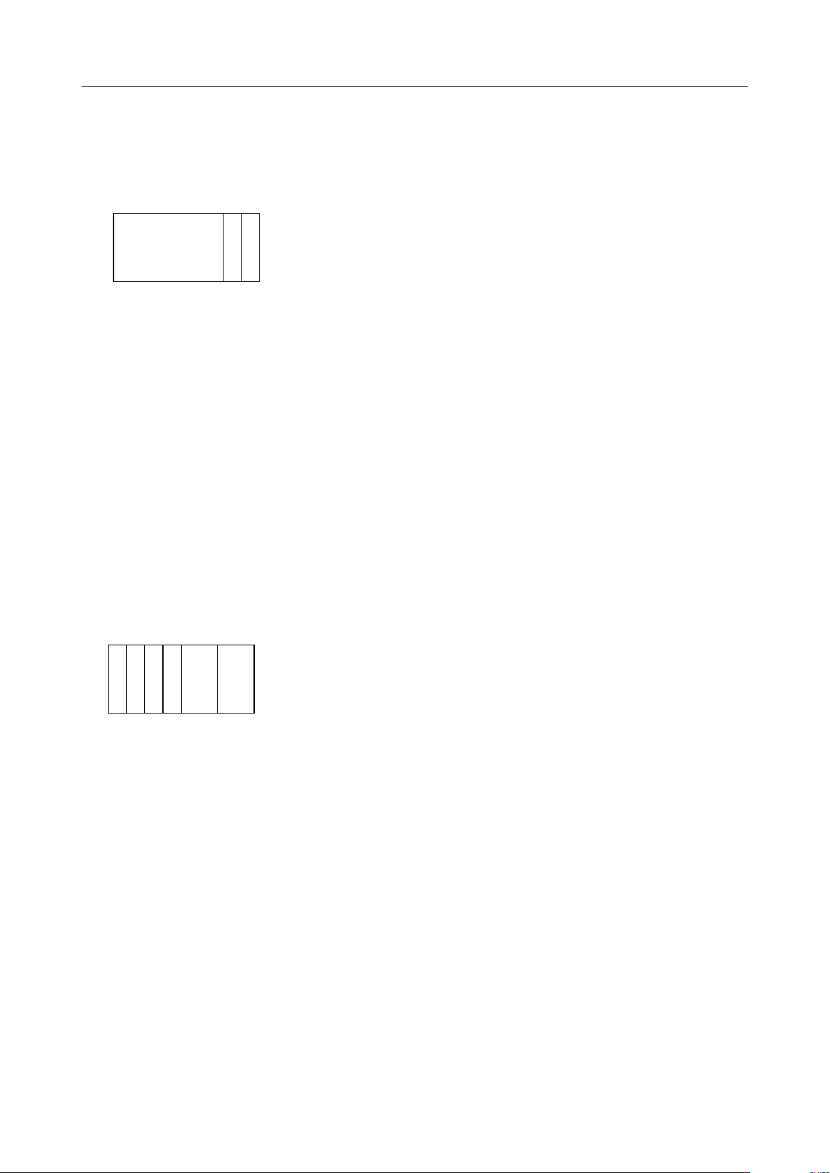
3.3 TSTS: Timer Status Register
This register provides TMR status.
0
17bit
T
T
D
000000
C
A
A
T
• bit[1] TDAT
0 : No timer interrupt request occurred (interval timer mode)
Divided clock output is "0" (divided clock mode)
1 : Timer interrupt request occurred (interval timer mode)
Divided clock output is "1" (divided clock mode)
• bit[0] TCA
MSM7630¡ Semiconductor
0 : Timer counter operation is suspended
1 : Timer counter is operating
3.4 TCMR: Command Register
This register sets TMR operation.
0
1234567bit
T
T
M
C
0TC
G
00
O
A
D
I
T
C
S
• bit[7] TCG
0 : Disable timer counter operation
1 : Enable timer counter operation
This bit will be "0" after reset.
• bit[5] TMOD
0 : Interval timer mode
1 : Divided clock mode
This bit will be "0" after reset.
85/95
Page 86

• bit[4] TCAI
0 : Disable auto-initialization of timer value register
1 : Enable auto-initialization of timer value register
This bit will be "0" after reset.
• bit[1:0] TCS
00 : Count clock F
01 : Count clock 4 F
10 : Count clock 16 F
11 : Count clock 64 F
These bits will be "00" after reset.
4. TMR Register Addresses
The MSM7630 has two timers. The register addresses for each are listed below.
MSM7630¡ Semiconductor
TMR1
TMR2
Timer Initial Value Register
Timer Value Register
Timer Status Register
Timer Command Register
Timer Initial Value Register
Timer Value Register
Timer Status Register
Timer Command Register
0xF8000000
0xF8000004
0xF8000008
0xF800000C
0xF8000010
0xF8000014
0xF8000018
0xF800001C
5. TMR Operation
5.1 Interval Timer Mode
In interval timer mode counting begins from the value set in the Timer Initial Value Register, and a
timer interrupt is generated to the CPU when the counter overflows.
1) Set the TCMR (Command Register) TCG bit to "0", disabling counting.
2) Set TCMR’s TCS bits to select the counter’s increment clock.
3) Set TCMR’s TMOD bit to "0", setting interval timer mode as the operating mode.
4) To generate periodic interrupts set TCMR’s TCAI bit to "1", which will set the counter to be loaded
with the value of the Timer Initial Value Register each time the counter overflows. For a one-shot
interrupt set the TCAI bit to "0".
5) Set the timer’s initial value in the Timer Initial Value Register TIR. Writing to this register will
simultaneously write the same value to the Timer Value Register TCR.
6) Write "1" to TCMR’s TCG bit to start counting. An interrupt will be generated when the counter
overflows.
7) To release the interrupt set the TSTS (Status Register) TDAT bit to "0" in software.
86/95
Page 87

MSM7630¡ Semiconductor
5.2 Divided Clock Mode
In divided clock mode counting begins from the value set in the Timer Initial Value Register, and the
divided clock output value inverts when the counter overflows.
1) Set the TCMR (Command Register) TCG bit to "0", disabling counting.
2) Set TCMR’s TCS bits to select the counter’s increment clock.
3) Set TCMR’s TMOD bit to "1", setting divided clock mode as the operating mode.
4) To generate a periodic divided clock set TCMR’s TCAI bit to "1", which will set the counter to be
loaded with the value of the Timer Initial Value Register each time the counter overflows. For a
one-shot divided clock set the TCAI bit to "0".
5) Set the timer’s initial value in the Timer Initial Value Register TIR. Writing to this register will
simultaneously write the same value to the Timer Value Register TCR.
6) Write "1" to TCMR’s TCG bit to start counting and generating a divided clock.
87/95
Page 88
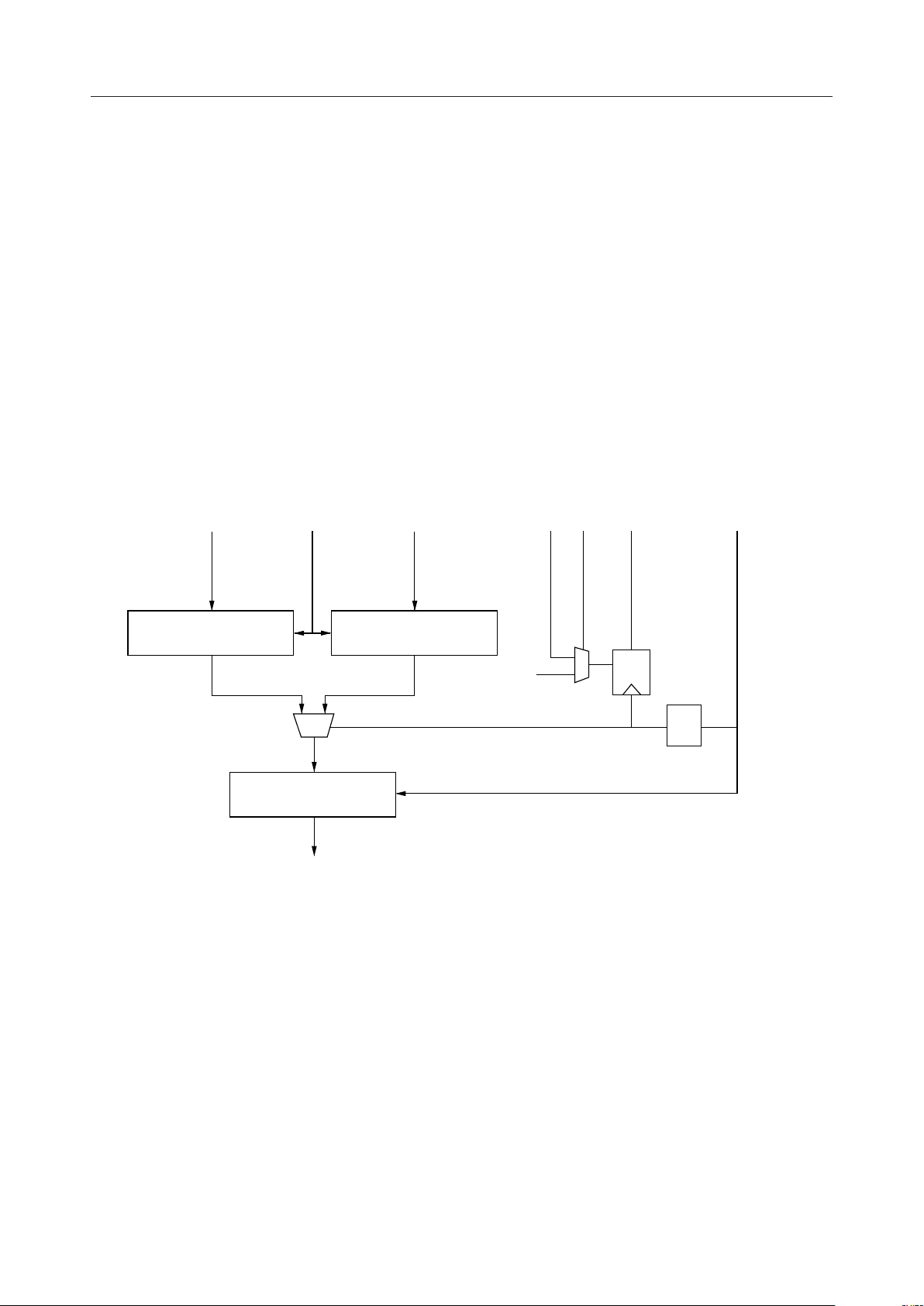
MSM7630¡ Semiconductor
Speech Data Registers
1. Features
This is a register group and control circuit used for speech output.
2. Speech Data Registers Functions
2.1 Speech Output Registers
These are 12-bit registers that store speech output data. There are two registers and one output
register configured to operate at the speech sampling frequency.
Use of two registers reduces the frequency of interrupt generation during waveform output, which
lightens the CPU load. The output stage is provided in the register, which corrects the inaccuracies
in the sampling frequencies that are caused by interrupts.
Interrupt to
DATA CLK DATA D WR
CPU
TMR2 output
12-bit REG 12-bit REG
1
1/2
12-bit REG
DAC
The two registers are in parallel, continuously written with D/A conversion data. The output
register reads the data from the two registers alternately in every sampling cycle.
The output level registers' clock is generated by TMR2. This clock is multiplied by 1/2 to output
interrupt signals. The interrupt signals are used to write the waveform output data to the speech
output registers.
Note the following when the MSM7576 mode (described later) is not used when using the speech
output registers :
– The TMR2 must be set to the divided clock mode.
– To write data to DAC1 and DAC2, write to DAC2 first, then DAC1.
– Do not clear the status register of the TMR2. If it is cleared by an interrupt routine, the sampling
frequency for the speech output will change.
88/95
Page 89
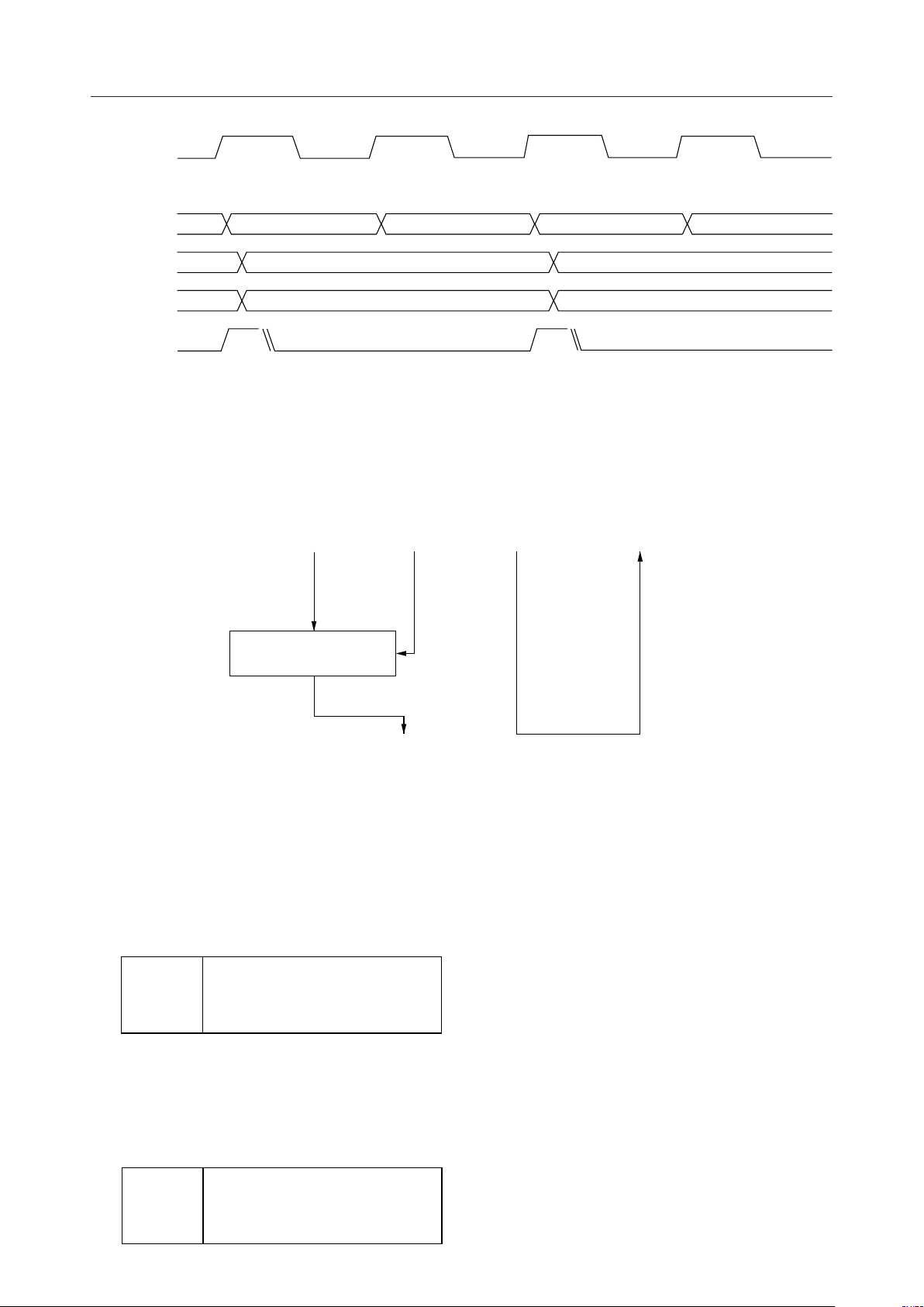
TMR2 output
MSM7630¡ Semiconductor
DAREGO
DAREG1
DAREG2
Interrupt to
CPU
0xxxxx 0x0000 0x0001 0x0002
0x0001
0x0000
0x0003
0x0002
2.2 MSM7576 Mode
This mode forces operation to be the same as MSM7576 operation. Interrupt signals from TMR2 are
output directly as interrupts to the CPU.
DATA CLK TMR2 output
12-bit REG
Interrupt to CPU
DAC
3. Speech Data Registers Details
3.1 DAC1: Speech Output Register 1
This register stores speech output data. It will be "000000000000" after reset.
15bit
0000
12 11
0
DAC1
3.2 DAC2: Speech Output Register 2
This register stores speech output data. It will be "000000000000" after reset.
15bit
12 11
0
0000
DAC2
89/95
Page 90

MSM7630¡ Semiconductor
3.3 DACO: D/A Conversion Register
This register stores data to be input to the D/A converter. It will be "000000000000" after reset.
15bit
0000
12 11
0
DACO
3.4 USTAT: Status Register
This register indicates whether or not the speech output registers/circuits have generated an
interrupt to the CPU.
Writing "0" to this register releases the interrupt from the speech output registers/circuits. In
MSM7576 mode USTAT will become "0" when the TMR2 interrupt is released.
0
17bit
U
0000000
S
T
A
T
3.5 UPORT: General Register
This is a general register. It will be "0" after reset.
0
17bit
U
0000000
P
O
R
T
3.6 MODE7576: MSM7576 Mode Select Register
This register sets MSM7576 mode. It will be "0" after reset.
0
17bit
M
0000000
O
D
E
90/95
Page 91
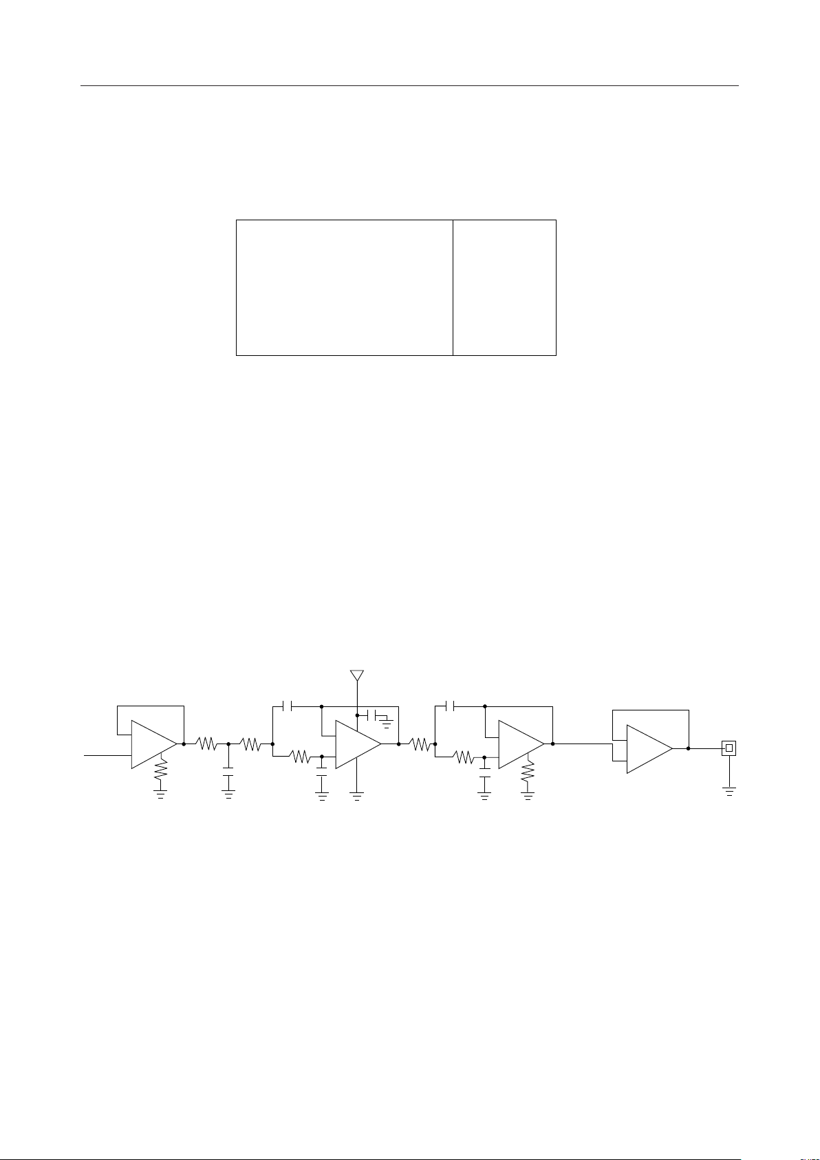
MSM7630¡ Semiconductor
4. Speech Output Registers Address Configuration
The addresses used by the speech output registers/circuits are assigned at 0x80000000. Accesses to
this space will be 3t access.
0x80000000Speech Output Register 1
0x80000004Speech Output Register 2
0x80000008D/A Conversion Register
0x8000000CStatus Register
0x80000010General Register
0x80000020MSM7576 Mode Select Register
Speech Output
1. Output Waveform from DAO1
The speech output pin directly outputs the output of the DA converter.
The output waveform from DAO1 will be a staircase synchronized to the sampling frequency.
Maximum output amplitude will be (4095/4096 ¥ VDD).
2. Output Filter
Because the output from DAO1 is a staircase described above, add a low-pass filter. The diagram
below shows a reference circuit for a Butterworth low-pass filter.
1200p
2
–
3
+
RR
1
8
1k
R
1000p 300p
MC14573P
0.1µ
15
4
–
14
R = 47k, f = 4.8 kHz (95 model: for 12 kHz sampling)
R = 36k, f = 6.4 kHz (96 model: for 16 kHz sampling)
R = 27k, f = 9.6 kHz (97 model: for 22 kHz sampling)
16
+
13
Butterworth low-pass filter
2200p
R
220p
11
–
10
12
+
9
1k
6
–
7
5
+
R
91/95
Page 92
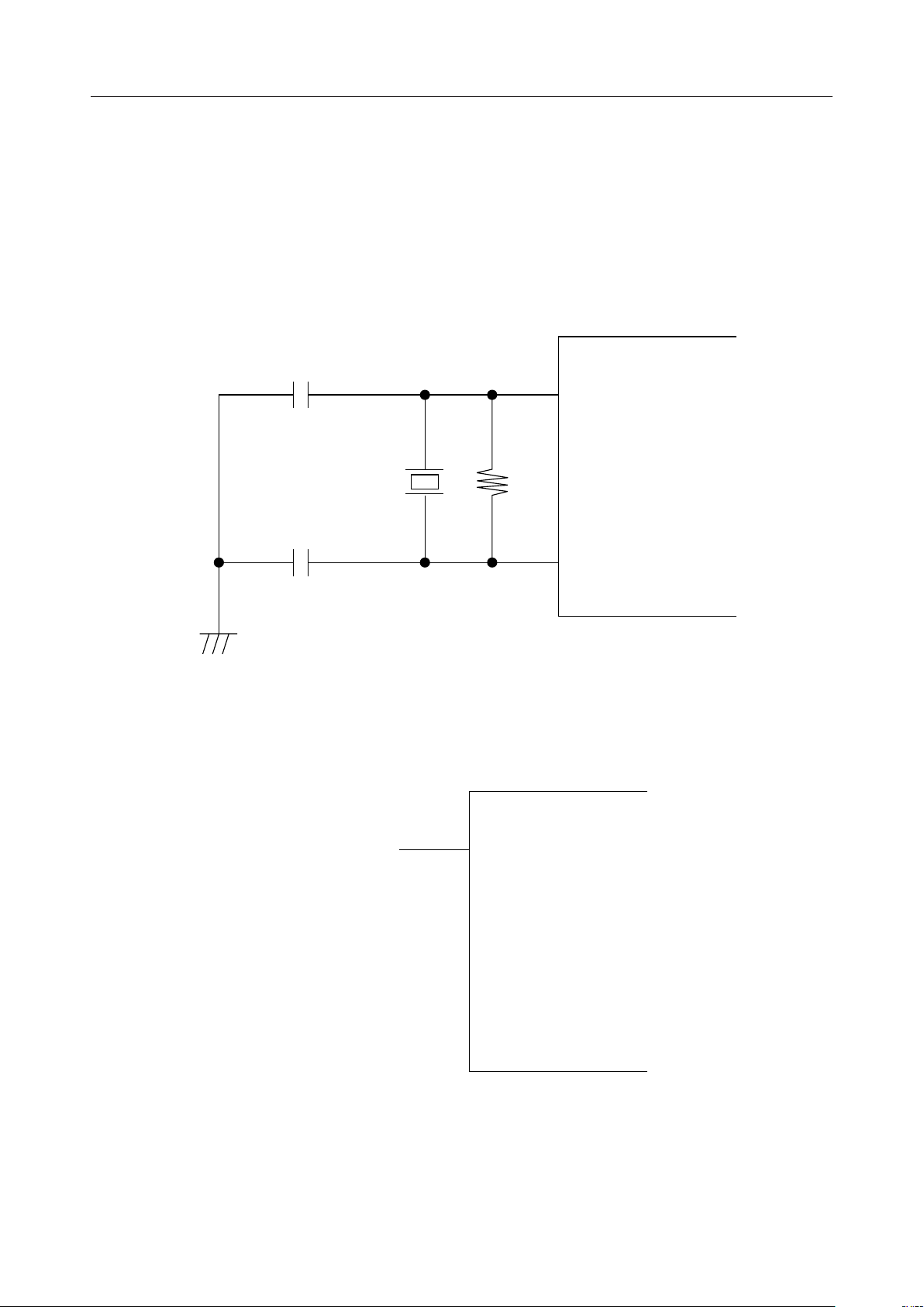
MSM7630¡ Semiconductor
Oscillation Circuit
There are two methods to generate the MSM7630 system clock: adding an external crystal oscillator
or supplying an external clock.
1. Crystal Oscillator
The diagram below shows a connection example for a crystal oscillator.
22 pF
CLK
Crystal
1 MW
22 pF
XO
GND
2. External Clock
The diagram below shows an example using an external clock.
MSM7630
MSM7630
External Clock
Open
CLK
XO
The external clock is input on the CLK pin. Leave the XO pin open.
92/95
Page 93
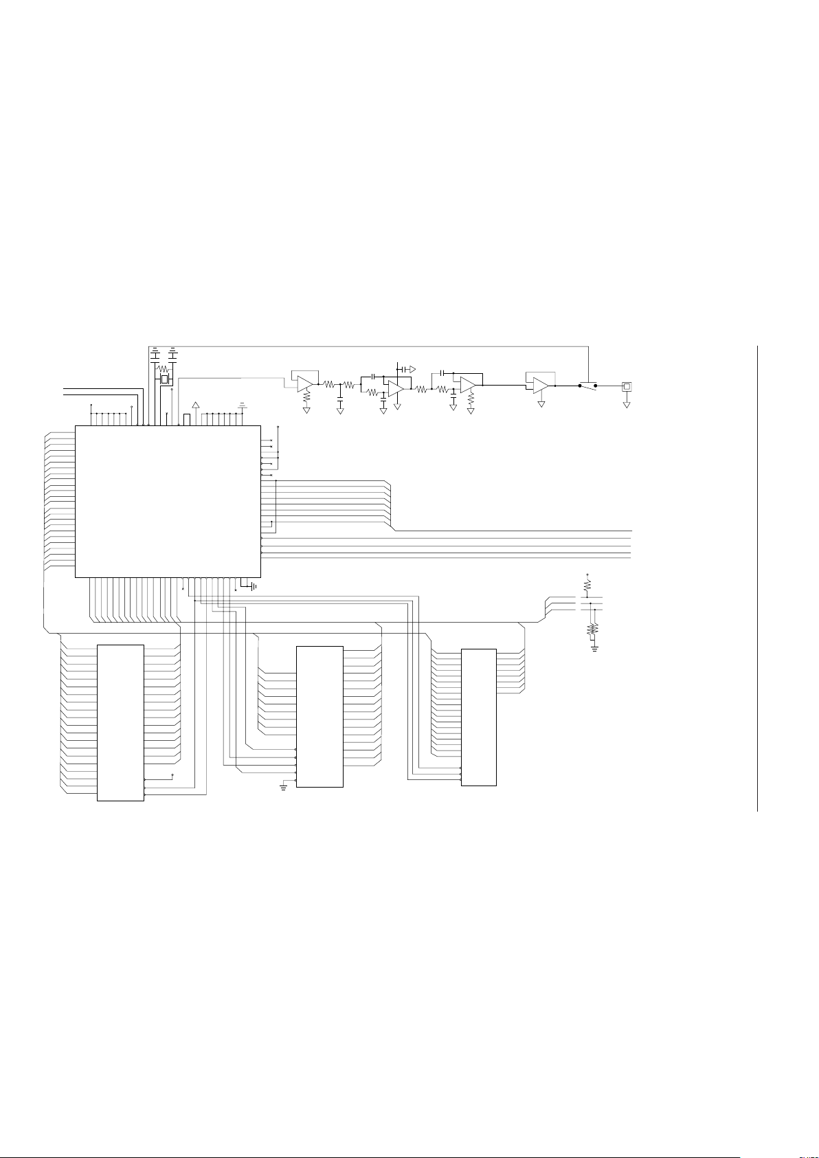
MSM7630¡ Semiconductor
93/95
SYSTEM CONFIGURATION EXAMPLE
Parallel Interface Application Example
+
–
+
–
+
–
+
–
3
2
8
1
RR
1k 1000p
R
1200p
100p
13
7
4
6
5
12
11
RR
2200p
1k
10
A +5 V
MC14573
8
220p
14
15
16
13
RCA Jack
STBY
RST
+3.3 V A +3.3 V
20 MHz
V
CC
1M
22p
22p
10244056728796
97
3
5
9092939196
100
99
98
1
2
17324864799495
V
DDVDDVDDVDDVDDVDDVDD
AV
DD
RST
STBY
UPORT
CLK
XO
CLKA
EXTINT
DAO1
TEST0
SG
AGND
GND
GND
GND
GND
GND
GND
GND
GND
D31
D30
D29
D28
D27
D26
D25
D24
D23
D22
D21
D20
D19
D18
D17
D16
WR1
WR0RDSRAM
ROMWERAS
CAS1
CAS0ASTSTM1
MSM7630
TSTM2
V
CC
D26
D25
D24
D31
D30
D29
D28
D27
D26
D25
D24
I/O7
I/O6
I/O5
I/O4
I/O3
I/O2
I/O1
I/O0
A18
A17
A16
A15
A14
A13
A12
A11
A10
A9
A8
A7
A6
A5
A4
A3
A2
A1
A0
WE
OE
CE
MSM29C401
A18
A17
A16
A15
A14
A13
A12
A11
A9
A8
A7
A6
A5
A4
A3
A2
A1
A0
A10
D15
D14
D13
D12
D11
D10
D9
D8
D7
D6
D5
D4
D3
D2
D1
D0
A8
A7
A6
A5
A4
A3
A2
A1
A0
RAS
UCAS
LCAS
WE
OE
MSM514260ZS
A9
A8
A7
A6
A5
A4
A3
A2
A1
Pull-up/down 10k
(when the bus capacitance is 100 pF)*
Text-to-Speech Conversion System Configuration Example
(Parallel Interface Application)
4Mb Flash ROM (x8)
4Mb DRAM (x16)
16Mb ROM (x16)
MSM27C1602
D15
D14
D13
D12
D11
D10
D9
D8
D7
D6
D5
D4
D3
D2
D1
D0
BYTE
OE
CE
A19
A18
A17
A16
A15
A14
A13
A12
A11
A10
A9
A8
A7
A6
A5
A4
A3
A2
A1
A0
V
CC
D31
D30
D29
D28
D27
D26
D25
D24
D23
D22
D21
D20
D19
D18
D17
D16
A19
A18
A17
A16
A15
A14
A13
A12
A11
A10
A9
A8
A7
A6
A5
A4
A3
A2
A1
A20
PD<7 : 0>
IOW
IOR
PCS
PA0
V
CC
54
51
53
46
50
49
47
30
31
33
34
35
36
37
38
45
43
44
42
41
39
SCLK
TXD
RXD
DSR
DTR
CTS
RTS
PD7
PD6
PD5
PD4
PD3
PD2
PD1
PD0
POBF
PIBF
PSTB
PACK
PCS
PIOA
A23
A22
A21
A20
A19
A18
A17
A16
A15
A14
A13
A12
A11
A10
A9
A8
A7
A6
A5
A4
A3
A2
A1
A0
A23
A22
A21
A20
A19
A18
A17
A16
A15
A14
A13
A12
A11
A10
A9
A8
A7
A6
A5
A4
A3
A2
A1
A0
85
84
83
82
81
80
78
77
76
75
74
73
71
70
69
68
67
66
65
63
62
61
60
59
121314151618192021222325262728
29
D31
D30
D29
D28
D27
D26
D25
D24
D23
D22
D21
D20
D19
D18
D17
D16
674119
555258
57888
89
Butterworth low-pass filter
R = 47k, f = 4.8 kHz (95 model: for 12 kHz sampling)
R = 36k, f = 6.4 kHz (96 model: for 16 kHz sampling)
R = 27k, f = 9.6 kHz (97 model: for 22 kHz sampling)
A
A
A
A
A
A
A
A
A
A
D31
D30
D29
D28
D27
D26
D25
D24
D23
D22
D21
D20
D19
D18
D17
D16
0.1µ
* Determine the value of each resistor
so that the bus will stabilize within 18 ms.
Page 94
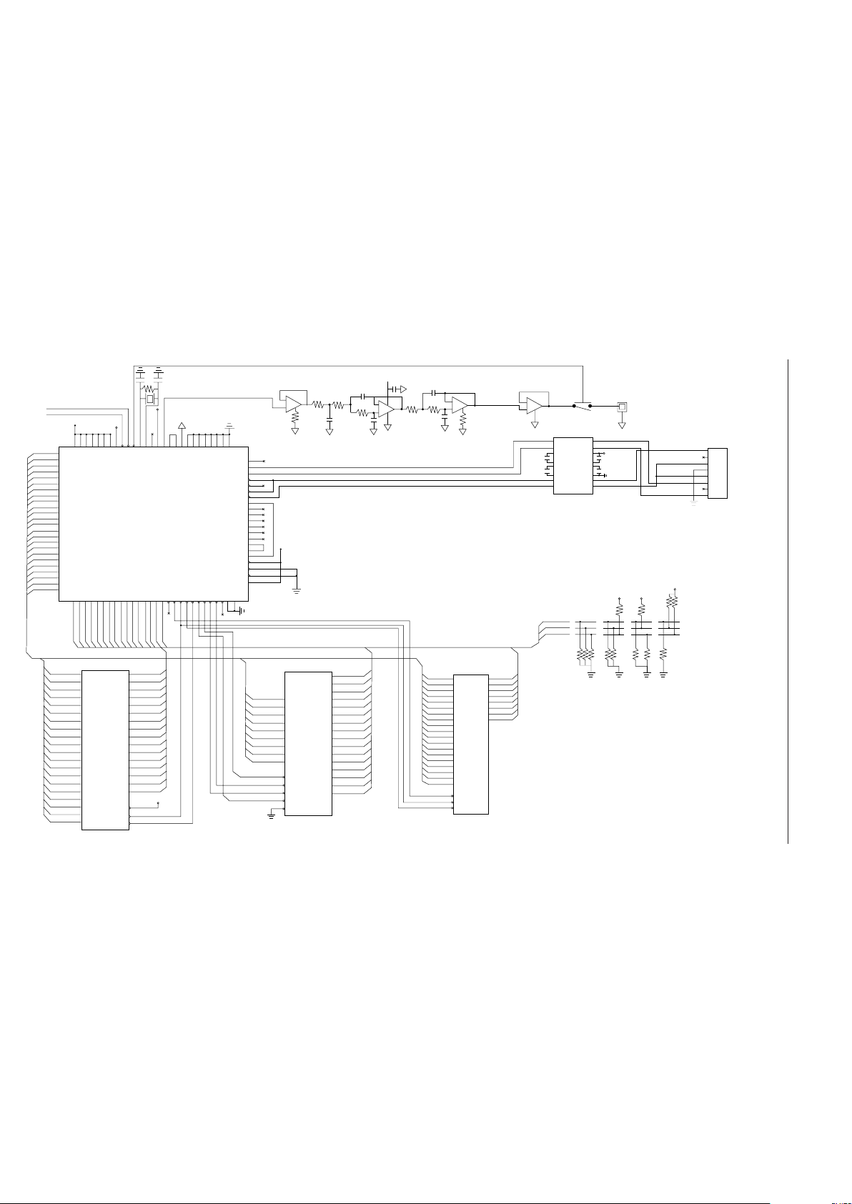
MSM7630¡ Semiconductor
94/95
Serial Interface Application Example
7
+
–
+
–
+
–
+
–
3
2
8
1
RR
1k 1000p
R
1200p
300p
13
7
4
6
5
12
11
RR
2200p
1k
10
A +5 V
MC14573
8
220p
14
15
16
13
RCA Jack
STBY
RST
+3.3 V A +3.3 V
20 MHz
1M
22p
22p
10244056728796
97
3
5
9092939186
100
99
98
1
2
17324864799495
V
DDVDDVDDVDDVDDVDDVDD
AV
DD
RST
STBY
UPORT
CLK
XO
CLKA
EXTINT
DAO1
TEST0
SG
AGND
GND
GND
GND
GND
GND
GND
GND
GND
D31
D30
D29
D28
D27
D26
D25
D24
D23
D22
D21
D20
D19
D18
D17
D16
WR1
WR0RDSRAM
ROMWERAS
CAS1
CAS0ASTSTM1
MSM7630
TSTM2
D26
D25
D24
D31
D30
D29
D28
D27
D26
D25
D24
I/O7
I/O6
I/O5
I/O4
I/O3
I/O2
I/O1
I/O0
A18
A17
A16
A15
A14
A13
A12
A11
A10
A9
A8
A7
A6
A5
A4
A3
A2
A1
A0
WE
OE
CE
MSM29C401
A18
A17
A16
A15
A14
A13
A12
A11
A9
A8
A7
A6
A5
A4
A3
A2
A1
A0
A10
D15
D14
D13
D12
D11
D10
D9
D8
D7
D6
D5
D4
D3
D2
D1
D0
A8
A7
A6
A5
A4
A3
A2
A1
A0
RAS
UCAS
LCAS
WE
OE
MSM514260ZS
A9
A8
A7
A6
A5
A4
A3
A2
A1
Text-to-Speech Conversion System Configuration Example
(Serial Interface Application)
4Mb Flash ROM (x8)
4Mb DRAM (x16)
16Mb ROM (x16)
MSM27C1602
D15
D14
D13
D12
D11
D10
D9
D8
D7
D6
D5
D4
D3
D2
D1
D0
BYTE
OE
CE
A19
A18
A17
A16
A15
A14
A13
A12
A11
A10
A9
A8
A7
A6
A5
A4
A3
A2
A1
A0
V
CC
D31
D30
D29
D28
D27
D26
D25
D24
D23
D22
D21
D20
D19
D18
D17
D16
A19
A18
A17
A16
A15
A14
A13
A12
A11
A10
A9
A8
A7
A6
A5
A4
A3
A2
A1
A20
54
51
53
46
50
49
47
30
31
33
34
35
36
37
38
45
43
44
42
41
39
SCLK
TXD
RXD
DSR
DTR
CTS
RTS
PD7
PD6
PD5
PD4
PD3
PD2
PD1
PD0
POBF
PIBF
PSTB
PACK
PCS
PIOA
A23
A22
A21
A20
A19
A18
A17
A16
A15
A14
A13
A12
A11
A10
A9
A8
A7
A6
A5
A4
A3
A2
A1
A0
A23
A22
A21
A20
A19
A18
A17
A16
A15
A14
A13
A12
A11
A10
A9
A8
A7
A6
A5
A4
A3
A2
A1
A0
85
84
83
82
81
80
78
77
76
75
74
73
71
70
69
68
67
66
65
63
62
61
60
59
121314151618192021222325262728
29
D31
D30
D29
D28
D27
D26
D25
D24
D23
D22
D21
D20
D19
D18
D17
D16
6
4119
555258
57888
89
Butterworth low-pass filter
R = 47k, f = 4.8 kHz (95 model: for 12 kHz sampling)
R = 36k, f = 6.4 kHz (96 model: for 16 kHz sampling)
R = 27k, f = 9.6 kHz (97 model: for 22 kHz sampling)
A
A
A
A
A
A
A
A
A
A
VCCV
CC
V
CC
2400 bps 4800 bps 9600 bps 19200 bps
V
CC
MAX232
T1IN T1OUT
R1OUT R1IN
C1+
C1–
C2+
C2–
R2OUT
T2IN
1µ
1µ
1
2
3
4
5
6
7
8
DIN8P
V
CC
1µ
1µ
V
CC
V+
V–
GND
R2IN
T2OUT
0.1µ
V
CC
D31
D30
D29
D28
D27
D26
D25
D24
D23
D22
D21
D20
D19
D18
D17
D16
Pull-up/down 10k
(when the bus capacitance is 100 pF)*
* Determine the value of each resistor
so that the bus will stabilize within 18 ms.
Page 95
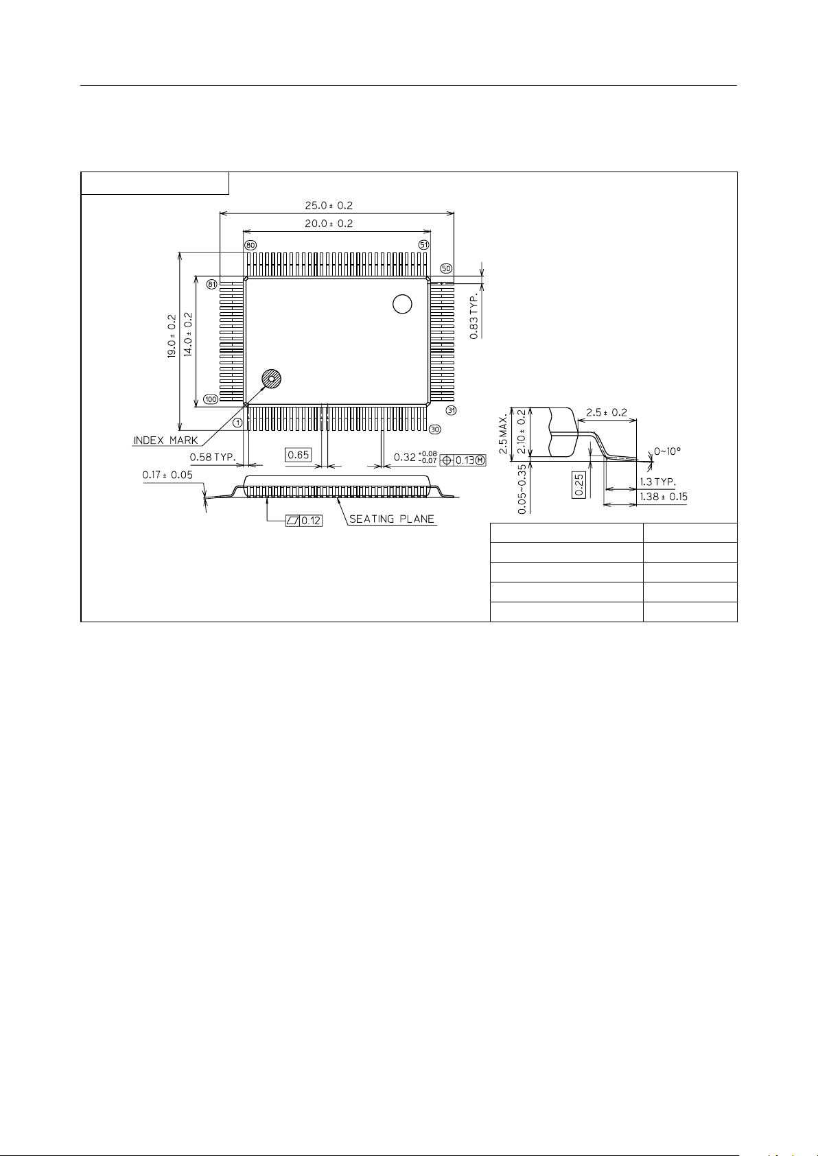
PACKAGE DIMENSIONS
QFP100-P-1420-0.65-BK
Mirror finish
MSM7630¡ Semiconductor
(Unit : mm)
Package material
Lead frame material
Pin treatment
Solder plate thickness
Package weight (g)
Epoxy resin
42 alloy
Solder plating
5 mm or more
1.29 TYP.
Notes for Mounting the Surface Mount Type Package
The SOP, QFP, TSOP, TQFP, LQFP, SOJ, QFJ (PLCC), SHP, and BGA are surface mount type
packages, which are very susceptible to heat in reflow mounting and humidity absorbed in
storage. Therefore, before you perform reflow mounting, contact Oki’s responsible sales person
on the product name, package name, pin number, package code and desired mounting conditions
(reflow method, temperature and times).
95/95
 Loading...