

Page 1

E2U0025-29-82
¡ Semiconductor
¡ Semiconductor
This version: Aug. 1999
Previous version: Jan. 1998
MSM7575
MSM7575
Multi-Function PCM CODEC
GENERAL DESCRIPTION
The MSM7575, developed for advanced digital cordless telephone systems, is a single channel
full duplex CODEC which performs mutual transcoding between the analog voice band signal
and the 64 kbps PCM serial data.
This device performs DTMF tone and several kinds of tone generation, transmit/receive data
mute and gain control, side-tone pass and its gain control, and VOX function.
Using advanced circuit technology, this device operates from a single 3 V power supply and
provides low power consumption.
FEATURES
••
• Single 3 V Power Supply Operation VDD: 2.7 V to ␣ 3.6 V
••
••
• Transmit/Receive Full-Duplex Single Channel Operation
••
••
• Transmit/Receive Synchronous Mode Only
••
••
• PCM Interface Data Format :
••
••
• Serial PCM Transmission Data Rate : 64 kbps to 2048 kbps
••
••
• Low Power Consumption
••
Operating Mode : 24 mW Typ. (V
Power-Down Mode : 0.03 mW Typ. (V
••
• Two Analog Input Amplifier Stages: Externally Gain Adjustable
••
••
• Analog Output Stage
••
••
• Master Clock Frequency : 9.600/19.200 MHz Selectable
••
••
• Transmit/Receive Mute, Transmit/Receive Programmable Gain Control
••
••
• Side Tone Path with Programmable Attenuation (8-step Level Adjustment)
••
••
• Built-in DTMF Tone Generator
••
••
• Built-in Various Ringing Tones Generator
••
••
• Built-in Various Ring Back Tone Generator
••
••
• Control by Serial MCU Interface
••
••
• Built-in VOX Control
••
Transmit side : Voice/Silence Signal Detect
Receive side : Background Noise Generation
••
• Built-in Op-amps and Analog Switches for Various Analog Interfaces.
••
••
• Package:
••
64-pin plastic QFP (QFP64-P-1414-0.80-BK)(Product name : 7575GS-BK)
A-law/µ-law/linear (2's complement) Selectable
= 3.0 V)
DD
= 3.0 V)
DD
Push-pull Drive (direct drive of 350 W␣ + 120 nF)
1/25
Page 2
2/25
¡ Semiconductor
MSM7575
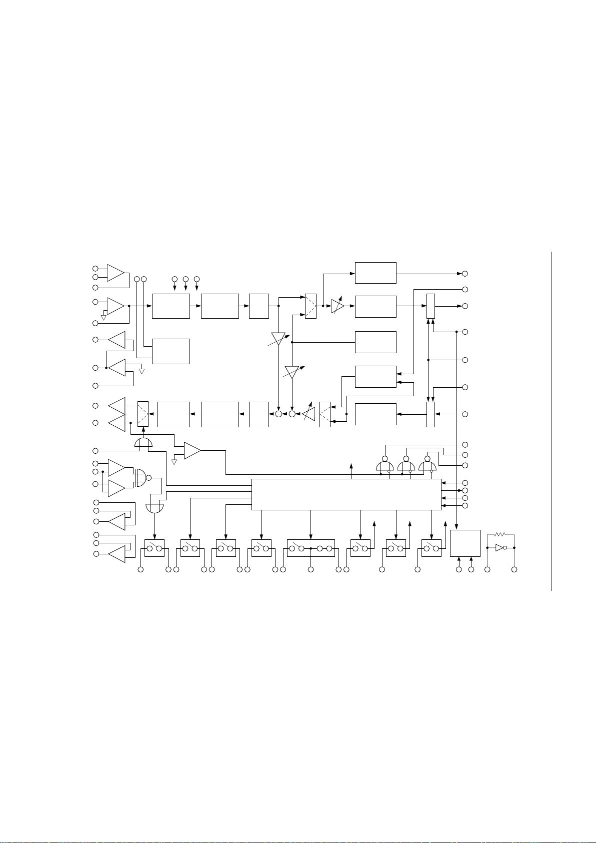
BLOCK DIAGRAM
AIN2
GSX2
VOXI
PCMSO
Prefilter
+
-
AIN1+
GSX1
AOUT-
BPF
P
/
S
XSYNC
RSYNC
PCMRI
S
/
P
Postfilter
LPF
BCLK
PWI
AOUT+
-1
VFRO
AIN1-
-1
VOXO
Compand
Voice Signal
Detect
A/D
D/A
++
EXCK
PDN/
RESET
MCU Interface
Clock/
Timing
ATT
ATT
ATT
+
-
-
+
SAO
-1
ATT
Expand
VREF
+
RINGC
AVIN
REF1
+
-
+
REF2
+
AIN3-
GSX3
AIN3+
+
AIN4-
GSX4
AIN4+
IO1
IO2
SW1
IO3
IO4
SW2
IO5
IO6
SW3
IO7
IO8
SW4
IO9
IO10
SW5
IO11
SW6
IO12
SW7
IO13
SW8
IO14
SW9
V
DD
V
DD
V
DD
MCK
X1
X2
DEN
DOUT
DIN
TOUT1
TOUT2
TOUT3
SGB
SG
AG
DG
V
DD
Tone GEN.
Back ground
Noise Gen.
To each circuit
Page 3
¡ Semiconductor
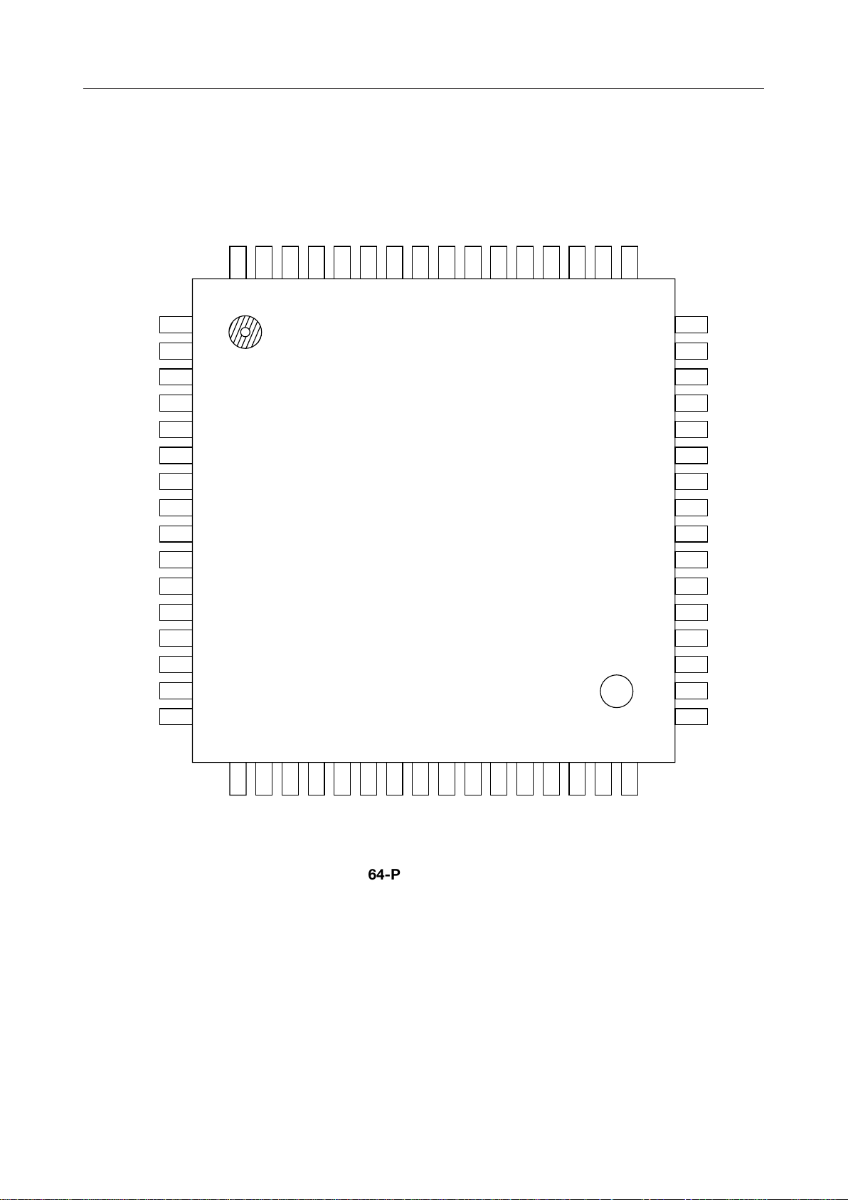
PIN CONFIGURATION (TOP VIEW)
MSM7575
VOXO
DOUT
DIN
EXCK
DEN
PCMRI
PCMSO
RSYNC
XSYNC
BCLK
DG
IO1
10
11
12
13
MCKX2NC
64
63
1
2
3
4
5
6
7
8
9
62
NC
61
X1
PDN/RESETNCTOUT3
60
59
58
57
TOUT2
TOUT1
56
55
RINGC
VDD
54
53
REF2
52
REF1
51
AVIN
50
NC
49
48VOXI
47
46
45
44
43
42
41
40
39
38
37
36
AOUT+
AOUT-
PWI
VFRO
SAO
GSX2
AIN2
GSX1
AIN1-
AIN1+
GSX4
AIN4-
AIN4+
14
IO2
15
IO3
16
IO4 AIN3+
NC : No connect pin
17
IO5
18
IO6
19
IO7
20
IO8
21
22
23
24
IO9
IO10
IO11
IO12
64-Pin Plastic QFP
25
IO13
26
IO14
27
NC
28
NC
29
NC
30
SGB
31
SG
32
AG
35
34
33
GSX3
AIN3-
3/25
Page 4
¡ Semiconductor
MSM7575
PIN AND FUNCTIONAL DESCRIPTIONS
AIN1+, AIN1–, AIN2, GSX1, GSX2
Transmit analog input and the output for transmit gain adjustment. The pin AIN1– (AIN2)
connects to the inverting input of the internal transmit amplifier, and the pin AIN1+ connects to
the non-inverting input of the internal transmit amplifier. The pin GSX1 (GSX2) connects to
output of the internal transmit amplifier. Gain adjustment should be referred to Fig. 1.
VFRO, AOUT+, AOUT–, PWI, SAO, RINGC
Used for the receive analog output and the output for receive gain adjustment. VFRO is an
output of the receive filter. AOUT+ and AOUT– are differential analog signal outputs which can
directly drive ZL = 350 W + 120 nF or the 1.2 kW load. Gain adjustment should be referred to Fig.
1.
The ORed signal with the control register data CR4-B5 and the external pin RINGC determines
the output pins (AOUT+ and AOUT- /SAO+ and SAO-) for the speech signal and an acoustic
component of the sounder tone, DTMF tone, R tone, F tone, various kinds of tones at either the
VFRO pin or the SAO pin.
Differential
Analog Input
0.1 mF
Vi
10 mF
+
–
Transmit Gain: V
= (R2/R1) ¥ (R4/R3)
Receive Gain: Vo/V
= 2 ¥ (R6/R5)
= 120 nF
Z
L
+ 350 W
C1
C1 R1
C2
V
R1
R3
GSX2
VFRO
O
R2
R4
/Vi
R5
R6
Differential
Analog
Output
R2
AIN1–
AIN1+
GSX1
SG
AIN2
GSX2
VFRO
PWI
AOUT–
AOUT+
–
+
–
+
–
+
–1
V
REF
to ENCODER
SELECT
from
DECODER
from MCU INT.
TOUT1
Sounder Output
Signal
SAO
RINGC
+1
Figure 1 Analog Input/Output Interface
+
–
TOUT2
TOUT3
from MCU INT.
4/25
Page 5
¡ Semiconductor
MSM7575
TOUT1, TOUT2, TOUT3
These are pins for outputs of the NOR gates whose inputs are the comparator output signal
between the SAO output level and the SG level, and each register signal stored by the MCU
interface.
The each output is NOR-gated with the comparator output and the invented signal of CR1-B7 at
TOUT3, the inverted signal of CR1-B6 at TOUT2, and the inverted signal of CR1-B5 at TOUT1.
AVIN, REF1, REF2
These pins are for inputs of two comparators internal to the device. AVIN is connected to each
non-inverting input of comparator1 and comparator2. REF1 is connected to an inverting input
of comparator1 and REF2 is connected to an inverting input of comparator2. The output of each
comparator is connected to the input of ENOR. The interval analog switch SW1 is ON/OFF
controlled by the output which is the logical OR of the ENOR and the CR5-B7 signal. When CR5B7 is at "0", the SW1 is turned to OFF if AVIN is within the voltage range of REF1 and REF2 and
the SW1 is turned to ON if AVIN is out of the voltage range of REF1 and REF2.
AIN3+, AIN3-, GSX3, AIN4+, AIN4-, GSX4
These pins are for inputs and outputs of the internal op-amps. Refer to BLOCK DIAGRAM for
the connection.
IO1 to IO14
These pins are for inputs and outputs of the internal analog switch. Refer to BLOCK DIAGRAM
and FUNCTIONAL DESCRIPTION for the connection and the control method.
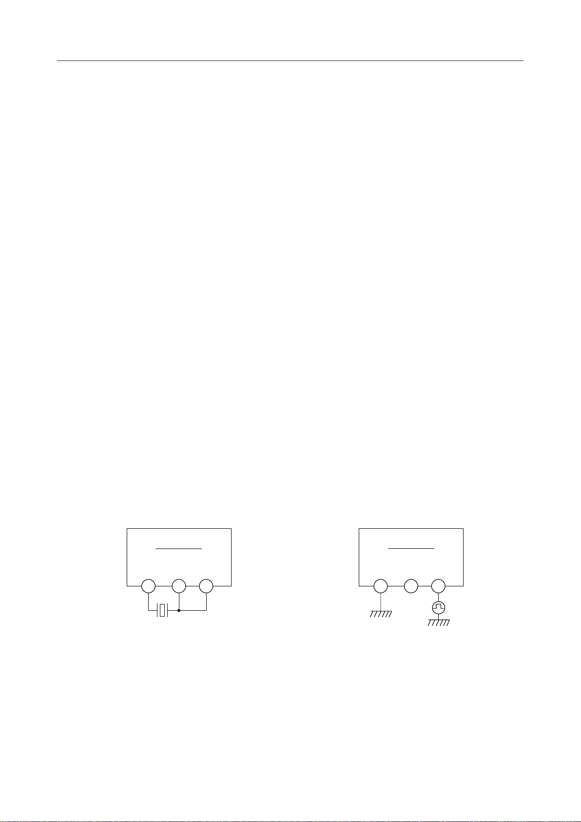
X1, X2
Crystal oscillator connection pins. X2 is for the clock output pin. When a conventional external
clock is used, X1 should be connected to the ground, X2 should be left open, and the clock should
be input to the MCK pin.
For the use of a self-oscilation circut
MSM7575
X1
X2
MCK
For the use of an external clock
MSM7575
X1
X2
MCK
9.6 MHz or
19.2 MHz
9.6 MHz or
19.2 MHz
Figure 2 Connection to a Crystal Oscillator or an External Clock
5/25
Page 6

¡ Semiconductor
MSM7575
SG, SGB
Analog signal ground output.
The output voltage is about 1.4 V. The bypass capacitors (10 µF in parallel with 0.1 µF ceramic
type) should be put between this pin and AG to get the specified noise characteristics. This
output voltage is 0 V during power-down.
AG
Analog ground.
DG
Digital ground.
This ground is separated from the analog signal ground(AG) in this device. The DG pin must be
kept as close to the AG pin possible on the PCB.
V
DD
+3 V power supply.
PDN/RESET
Power down and reset control input.
“L” level makes the whole chip enter to power down state, and, at the same time, all of control
register data are reset to the initial state. Set this pin to “H” level during normal operating mode.
The power down state is controlled by a logical OR with CR0-B5 of the control register. When
using the pin PDN/RESET for the power down and reset control, CR0-B5 should be set to digital
“0”.
MCK
Master clock input.
The frequency must be 9.6 MHz or 19.2 MHz. The applied clock frequency is selected by the
control register data CR0-B6. The master clock signal is allowed to be asynchronous with BCLK,
XSYNC, and RSYNC.
PCMSO
Transmit PCM data output.
This PCM output signal is output from MSB in synchronization with the rising edge of BCLK or
XSYNC. A pull-up resistor must be connected to this pin, because this output is configuared as
an open drain.
During power down, this output is at high impedance state.
6/25
Page 7
¡ Semiconductor
MSM7575
PCMRI
Receive PCM data input.
This PCM input signal is shifted on the falling edge of BCLK and input from MSB.
BCLK
Shift clock input for the PCM data (PCMSO, PCMRI).
The frequency is set in the range of 64 kHz to 2048 kHz.
XSYNC
8 kHz synchronous signal input for Transmit PCM data.
This signal should be synchronized with BCLK. XSYNC is used for indicating MSB of the
transmit serial PCM.
Be sure to input the XSYNC signal because it is also used as the input of the timing circuit and
the clock source of the tone generator.
RSYNC
8 kHz synchronous signal input for Receive PCM data.
This signal should be synchronized with BCLK signal. RSYNC is used for indicating the MSB
of the receive serial PCM.
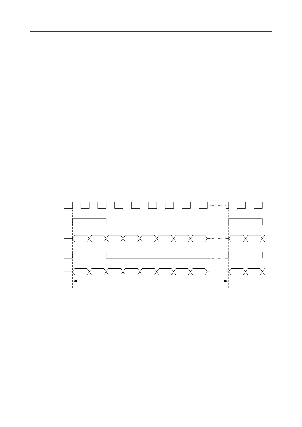
BCLK
XSYNC
PCMSO
RSYNC
PCMRI
MSB LSB
MSB LSB
8kHz
(125ms)
Figure 3 PCM Interface Basic Timing Diagram
7/25
Page 8
¡ Semiconductor
MSM7575
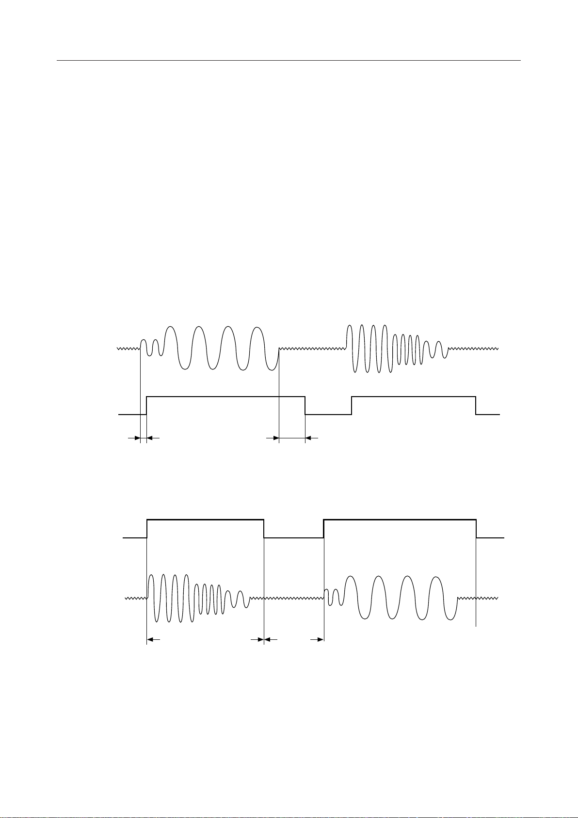
VOXO
Transmit VOX function signal output.
VOX function is to recognize the presence or absence of the transmit voice signal by detecting the
signal energy. “H” and “L” levels set to this pin correspond to the presence and the absence,
respectively. This result appears also at the register data CR7-B7. The signal energy detect
threshold is set by the control register data CR6-B6, B5.
VOXI
Signal input for receive VOX function.
The “H” level at VOXI indicates the presence of voice signal, the decoder block processes normal
receive signal, and the voice signal appears at analog output pins . The “L” level indicates the
absence of voice signal, the background noise generated in this device is transferred to the analog
output pins. The background noise amplitude is set by the control register CR6. Because this
signal is ORed with the register data CR6-B3, the control register data CR6-B3 should be set to
digital “0”.
Voice Input
GSX2
VOXO
VOXI
Voice Output
VFRO
(Absence)
(Presence)
T
VXON
Presence
Detect
T
VXOFF
Absence
Detect (Hang-over time)
(a) Transmit VOX Function Timing Diagram
(Absence)
(Presence)
(Presence)
(Presence)
Normal Voice Signal
Decoded Time period
Background
Noise
(b) Receive VOX Function (CR6-B3: digital "0") Timing Diagram
Note: VOXO, VOXI function become valid when setting CR6-B7 to digital “1”.
Figure 4 VOX Function
8/25
Page 9

¡ Semiconductor
(b)
,
MSM7575
DEN , EXCK, DIN, DOUT
Serial control ports for MCU interface. Reading and writing data is performed by an external
MCU through these pins. Total 8 registers with 8 bits are provided on the devices.
DEN is the “Enable” control signal input, EXCK is the data shift clock input, DIN is the address
and data input, and DOUT is the data output from which inverted data of the contents of the
register is output.
Fig.5 shows the input or output timing diagram.
DEN
EXCK
W
A2
DIN
A1 A0 B7 B6 B5 B4 B3 B2 B1 B0
DOUT
DEN
EXCK
DIN
DOUT
R A2A1A0
High Impedance
Figure 5 MCU Interface Input/Output Timing
Register map is shown below.
Name
CR0
CR1
CR2
CR3
CR4
CR5
Address
A2 A1 A0
000
001
010
011
100
101
B7 B6 B5 B4 B3 B2 B1 B0
A/m
SEL
TOUT3
-CONT
TX
ON/OFFTXGAIN2TXGAIN1TXGAIN0
Side Tone
GAIN2
DTMF/
OTHERS
SEL
SW7-
CONT
High Impedance
(a) Write Data Timing Diagram
B7 B6 B5 B4 B3 B2 B1 B0
Read Data Timing Diagram
Table-1
Control and Detect Data
MCK
SEL
TOUT2
-CONT
Side Tone
GAIN1
TONE
SEND
SW8-
CONT
PDN
ALL
TOUT1
-CONT
Side Tone
GAIN0
SAO/
VFRO
SW9-
CONT
TONE
ON/OFF
TONE4 TONE3 TONE2 TONE1 TONE0
SW5&
SW6-CONT
PDN
TX
— — — — RX PAD
PDN
RX
RX
ON/OFFRXGAIN2RXGAIN1
TONE
GAIN3
SW4-
CONT
— LNR
TONE
GAIN2
SW3-
CONT
TONE
GAIN1
SW2-
CONT
PDN
SAO/AOUT
RX
GAIN0
TONE
GAIN0
SW1-
CONT
R/W
R/W
R/W
R/W
R/W
R/W
R/W
CR6
CR7
110
111
VOX
ON/OFFONLVL1
VOX
OUT
TX NOISE
LVL1
ON
LVL0
TX NOISE
LVL0
IN
RX NOISE
LEVEL SEL
OFF
TIME
—————
VOX
RX NOISE
LVL1
RX NOISE
LVL0
R/W
R
R/W : Enable to read/write R : Read only register.
9/25
Page 10

¡ Semiconductor
ABSOLUTE MAXIMUM RATINGS
MSM7575
Parameter
Power Supply Voltage
Analog Input Voltage
Digital Input Voltage
Operating Temperature
Storage Temperature
Symbol
V
DD
V
AIN
V
DIN
T
op
T
STG
Condition
—
—
—
—
—
RECOMMENDED OPERATING CONDITIONS
Parameter
Power Supply Voltage
Operating Temperature Range
Input High Voltage
Input Low Voltage
Master Clock Frequency
Bit Clock Freqency
Synchronous Signal Frequncy
Clock Duty Ratio
Digital Input Rise Time
Digital Input Fall Time
Transmit Sync Signal Setting Time
Receive Sync Signal Setting Time
Synchronous Signal Width
PCM Set-up Time
PCM Hold Time
Digital Output Load
Bypass Capacitors for SG
Symbol
V
DD
Ta
V
IH
V
IL
f
MCK1
f
MCK2
f
BCK
f
SYNC
D
C
t
Ir
t
If
t
XS
t
SX
t
RS
t
SR
t
WS
t
DS
t
DH
R
DL
C
DL
C
SG
Condition
—
—
MCK, XSYNC, RSYNC, PCMRI,
RINGC, BCLK, VOXI,
PDN/RESET, DEN, EXCK, DIN
MCK, XSYNC, RSYNC, PCMRI,
RINGC, BCLK, VOXI,
PDN/RESET, DEN, EXCK, DIN
MCK (CR0–B6 = "0")
MCK (CR0–B6 = "0")
BCLK
XSYNC, RSYNC
MCK, BCLK, EXCK
MCK, XSYNC, RSYNC, PCMRI,
RINGC, BCLK, VOXI,
PDN/RESET, DEN, EXCK, DIN
MCK, XSYNC, RSYNC, PCMRI,
RINGC, BCLK, VOXI,
PDN/RESET, DEN, EXCK, DIN
BCLK to XSYNC
XSYNC to BCLK
BCLK to RSYNC
RSYNC to BCLK
XSYNC, RSYNC
—
—
PCMSO (Pull-up Resistor)
TOUT1, TOUT2, TOUT3,
PCMSO, VOXO, DOUT
SG to AG
Rating
–0.3 to +5
– 0.3 to V
–0.3 to V
DD
DD
+ 0.3
+ 0.3
–30 to +85
–55 to +150
Min. Typ. Max. Unit
+2.7
–25
0.45 ¥ V
0
–0.01%
–0.01%
64
—
30
—
—
100
100
100
100
1 BCLK
100
100
500
—
10 + 0.1
DD
—
+25
—
—
9.600
19.200
—
8.0
50
—
—
—
—
—
—
—
—
—
—
—
—
+3.6
+70
V
DD
0.16 ¥ V
+0.01%
+0.01%
2048
—
70
50
50
—
—
—
—
100
—
—
—
100
—
DD
Unit
V
V
V
°C
°C
V
°C
V
V
MHz
MHz
kHz
kHz
%
ns
ns
ns
ns
ns
ns
ms
ns
ns
W
pF
mF
10/25
Page 11

¡ Semiconductor
ELECTRICAL CHARACTERISTICS
DC and Digital Interface Characteristics
Parameter
Power Supply Current
Input High Voltage
Input Low Voltage
Input Leakage Current
Output High Voltage V
Output Low Voltage
Output Leakage Current
Input Capacitance
Output Resistance
Symbol
I
DD1
I
DD2
V
IH
V
IL
I
IH
I
IL
OH
V
OL
I
O
C
IN
R
OSG
Operating Mode,
Power Down Mode,
VI = V
DD
VI = 0 V
I
0.4 mA
OH =
1 mA
I
OH =
1 LSTTL, Pull-up: 500 W
PCMSO
SG —2550kW
MSM7575
2.7 V to 3.6 V, Ta = –25°C to +70°C)
(V
DD =
Condition
(V
(V
—
—
DD
DD
3.0 V)
=
=
3.0 V)
Min.
—
—
0.45¥V
0.0
—
—
0.5 ¥ V
0.8 ¥ V
0.0
—
— —5—pF
DD
DD
DD
Typ.
8
0.01
—
—
—
—
—
—
0.2
—
Max.
6
0.1
V
DD
0.16¥V
2.0
0.5
V
DD
V
DD
0.4
10
Unit
mA
mA
DD
mA
mA
mA
V
V
V
V
V
Transmit Analog Interface Characteristics
2.7 V to 3.6 V, Ta = –25°C to +70°C)
(V
DD =
Parameter
Input Resistance
Output Load Resistance
Output Load Capacitance
Output Amplitude
Input Offset Voltage
Symbol
R
INX
R
LGX
C
LGX
V
OGX
V
OFGX
Condition
AIN1+ , AIN1– , AIN2
GSX1, GSX2
GSX1, GSX2
GSX1, GSX2, R
= 20 kW
L
Pre–OPAMPs
Min.
10
20
—
—
–20
*1 –7.7 dBm (600 W) = 0 dBm0, + 3.17 dBm0 = 1.30 VPP (m-law Selected)
Typ.
—
—
—
—
—
Max.
—
—
100
1.30 (*1)
20
Unit
MW
kW
pF
V
PP
mV
11/25
Page 12

¡ Semiconductor
Receive Analog Interface Characteristics
Parameter
Input Resistance
Output Load Resistance
Output Load Capacitance
Output Voltage Level
Offset Voltage
Comparator Input Voltage Range
Analog Switch "ON" Resistance
Symbol
R
INPW
R
LVF
R
LAO
C
LVF
C
LAO
V
OVF
V
OAO
V
OFVF
V
OFAO
G
DB
R
SW
PWI, AIN3+/–, AIN4+/–, REF1,
REF2, AVIN
VFRO, SAO
AOUT+, AOUT–, GSX3, GSX4
VFRO, SAO
AOUT+, AOUT–, GSX3, GSX4
VFRO, SAO
AOUT+,
AOUT–,
GSX3,
GSX4
VFRO, SAO
AOUT+, AOUT– (Gain = 0 dB,
Power amp only)
AVIN, REF1, REF2
IO1-IO2, IO3-IO4, IO5-IO6,
IO7-IO8, IO9-IO10, IO10-IO11,
IO12-
VDD, IO13-
Condition
R
= 20 kW
L
R
= 1.2 kW
L
= 350 kW
Z
L
+ 120 nF(See Fig.1)
GSX3, GSX4
VDD, IO14-
MSM7575
(V
2.7 V to 3.6 V, Ta = –25°C to +70°C)
DD =
Min.
10
20
1.2
—
—
—
—
—— V
–100
–20
0.85 — VDD–0.75 —
100 — 400 W
V
DD
Typ.
—
—
—
—
—
—
—
—
—
Max.
—
—
—
100
100
1.30 (*1)
1.30 (*1)
1.30 (*1)
100
20
Unit
MW
kW
kW
pF
pF
V
PP
V
PP
PP
mV
mV
*1 –7.7 dBm (600 W) = 0 dBm0, + 3.17 dBm0 = 1.30 VPP (m-law Selected)
12/25
Page 13

¡ Semiconductor
AC Chracteristics
Parameter
Transmit Frequency
Response
Receive Frequency
Responce
Transmit Signal
to Distortion Ratio
Receive Signal
to Distortion Ratio
Transmit Gain
Tracking
Receive Gain
Tracking
Idle Channel Noise
Absolute Signal
Amplitude
(V
2.7 V to 3.6 V, Ta = –25°C to +70°C)
DD =
Condition
Symbol
Freq.
Level
Others
Min.
Typ.
(dBm0)(Hz)
L
T1
0 to 60
T2
300 to 3000 –0.15 — 0.20 dB
T3
T4
T5
T6
R1
R2
R3
R4
R5
1020 Reference dB
0
—
3300 –0.15 — 0.80 dB
3400 0 — 0.80 dB
3968.75 13 — — dB
0 to 3000 –0.15 — 0.20 dB
1020 Reference dB
3300 –0.15 — 0.80 dB0
—
3400 0 — 0.80 dB
3968.75 13 — — dB
L
L
L
L
L
L
L
L
L
L
OSS
OSS
OSS
OSS
OSS
OSS
OSS
OSS
OSS
OSS
OSS
SD T1 35 —3
SD T2 35 —0
SD T3 35 —–30
1020
(*2)
SD T4
SD T5 23 —–45
SD R1 —3
SD R2 —0
SD R3 —–30
1020
(*2)
SD R4
SD R5 —–45
GT T1 –0.2 0.2
GT T2 Reference
GT T3 1020 –0.2 0.2–40
GT T4 –0.5 0.5
GT T5 –1.2 1.2
GT R1 –0.2 0.2
GT R2 Reference
GT R3 1020 –0.2 0.2
GT R4 –0.5 0.5
GT R5 –1.2 1.2
N
IDLT
———
3
–10
–50
–55
3
–10
–40
–50
–55
AIN = SG
—
—
(*2)
25
28 —–40
35
35
35
28
23
—
—
—
—
—
—
—
—
—
—
—
—
—
—
—
—
—
—
—
(–75.7)
(*2)
N
IDLR
——
—
(*3)
—
(–79.7)
0.320
A
VT
1020
0
GSX2
0.285
(*4)
0.320
A
VR
VFRO
0.285
(*4)
MSM7575
Max.—Unit
dB
dB
dB
dB
dB
dB
dB
dB
dB
—–40
–68
–72
0.359
0.359
dB
dB
dB
dB
dB
dB
dB
dB
dB
dB
dB
dB
dBmOp
(dBmp)
Vrms
Vrms
13/25
Page 14

¡ Semiconductor
AC Characteristics (Continued)
Parameter
Power Supply Noise
Rejection Ratio
Digital Input/Output
Setting Time
Serial Port Digital
Input/Output Setting
Time
Symbol
P
SRRT
P
SRRR
t
SDX
t
XD1
t
XD2
t
XD3
t
M1
t
M2
t
M3
t
M4
t
M5
t
M6
t
M7
t
M8
t
M9
t
M10
t
M11
F
EXCK
Noise Freq.
: 0 to 50 kHz
Freq.
—
(V
2.7 V to 3.6 V, Ta = –25°C to +70°C)
DD =
Condition
Level Min. Typ. Max. Unit
(dBm0)(Hz)
Others
Noise Level
30——dB
—
: 50 mV
PP
30——dB
200
0—
*5(100)
200
0—
1LSTTL + 100 pF
pull-up: 500 W
See
Fig.4
*5(100)
200
0—
*5(100)
200
0—
*5(100)
50——ns
50——ns
50——ns
50——ns
100 — — ns
See
C
Load
= 100 pF—
Fig.7
50——ns
50——ns
0 — 50 ns
50——ns
50——ns
0 — 50 ns
——10MHz—— EXCKShift Clock Frequency
MSM7575
ns
ns
ns
ns
*2 Use the P-message weighted filter
*3 PCMRI input code "11010101"(A-law)
"11111111"(m-law)
*4 0.320 Vrms = 0 dBm0 = –7.7 dBm
*5 Value in ( ) is for C
= 10 pF Pull-up £ 20 kW
Load
Note: All ADPCM coder and decoder characteristics comply with ITU-T Recommendation
G.721.
14/25
Page 15

¡ Semiconductor
AC Characteristics (DTMF and Other Tones)
Parameter
Frequency Difference
Original (reference)
Tone Signal Level
*6
Relative Level of
DTMF Tones
Symbol
D
D
V
DTMF Tones –7 — +7 Hz
FT1
Other Tones
FT2
TL
Transmit
TH
RL
Tones
V
V
Receive
V
Tones
RH
DTMFVTH/VTL
Condition
DTMF (Low)
DTMF (High)
and Other Tones
DTMF (Low)
DTMF (High)
and Other Tones
, VRH/V
RL
*6 Not contain the setting value of the programmable gain
2.7 V to 3.6 V, Ta = –25°C to +70°C)
(V
DD =
Min. Typ. Max. Unit
–7—+7Hz
–18
–16
–4
–2
+1 dBm0R
–16
–14
–2
0
+2
MSM7575
–14
–12
+2
+3
dBm0
dBm0
0
dBm0
dBm0
AC Characteristics (Programmable Gain Stages)
Parameter
Gain Accuracy
Symbol
D
G
All gain stages, to programmed value –1 0 +1 dB
Condition
AC Characteristics (VOX Function)
Parameter
Transmit VOX Detect Time
(Voice signal ON/OFF detect time
Transmit VOX Detect Level
Accuracy
(Threshold Level)
Symbol
t
VXON
t
)
VXOF
D
VX
Condition
OFF Æ ON — 5 — ms
ON Æ OFF
VOXO,
Fig.4
To the setting of detect level
by CR6-B6, B5.
2.7 V to 3.6 V, Ta = –25°C to +70°C)
(V
DD =
Min. Typ. Max. Unit
(V
2.7 V to 3.6 V, Ta = –25°C to +70°C)
DD =
Min. Typ. Max. Unit
150/310 160/320 170/330 ms
–2.5 dB
0 +2.5
15/25
Page 16

¡ Semiconductor
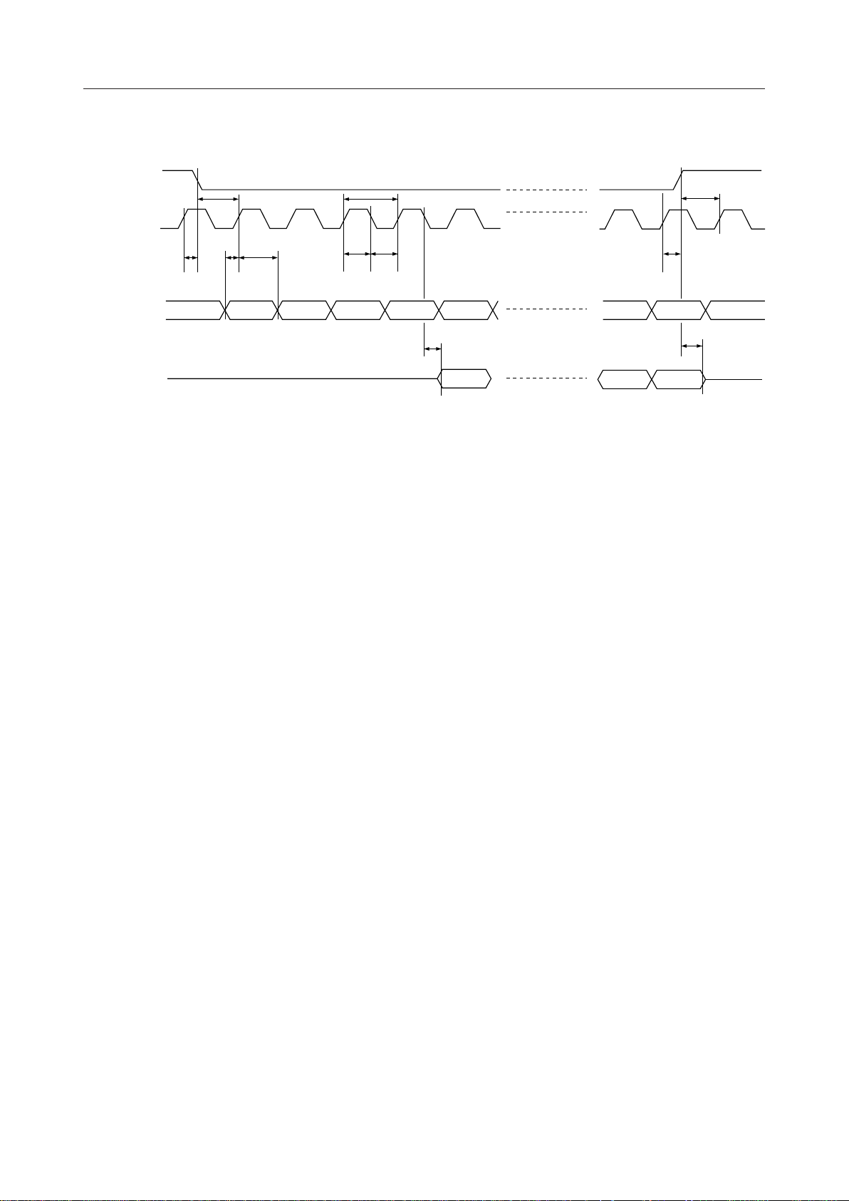
TIMING DIAGRAM
Transmit Side PCM Data Interface
MSM7575
BCLK
XSYNC
PCMSO
0
t
XS
12345678910
t
SX
t
XD1
t
t
WS
XD2
MSB LSB
t
SDX
Receive Side PCM Data Interface
BCLK
RSYNC
PCMRI
0
t
RS
12345678910
t
SR
t
DS
t
WS
t
DH
MSB
Figure 6 PCM Data Interface
LSB
t
XD3
16/25
Page 17
¡ Semiconductor
Serial Port Data Transfer for MCU Interface
DEN
t
M5
EXCK
t
M2
123456
11 12
MSM7575
t
M10
DIN
DOUT
t
M1tM3
t
t
M4
M6
t
M7
W/R A2 A1 A0 B7
t
M8
B7
Figure 7 MCU Interface
t
M9
B1 B0
B1 B0
t
M11
17/25
Page 18

¡ Semiconductor
MSM7575
FUNCTIONAL DESCRIPTION
Control Registers
(1) CR0 (Basic operating mode)
B7 B6 B5 B4 B3 B2 B1 B0
CR0 MCK SEL PDN ALL PDN TX PDN RX — LNR
Initial Value
A/m SEL
00000000
Note) "Initial": Reset state by PDN/RESET
B7 ...PCM Companding law select: 0/µ-law, 1/A-law
B6 ...Master clock frequency select: 0/9.600 MHz, 1/19.200 MHz
B5 ...Power down (whole system): 0/Power on, 1/Power down
When using this data for power down control, pin PDN/RESET should be set at
“H”level. The control registers are not reset by this signal.
B4 ...Power down (Transmit only): 0/Power on, 1/Power down
B3 ...Power down (Receive only including the op-amps of GSX3, GSX4 and comparator): 0/
Power on, 1/Power down
B2 ...Not used
B1 ...PCM interface linear code select:
0/Companding law selected by CR0-B7
1/14-bit Linear code (2's complement) in spite of the value of CR0-B7
B0 ...Power Down for Sounder output amps: (SAO), or Receiver output amp (AOUT, VFRO ):
When this data is set to digital “1”, the circut which is not selected by CR4-B5 are at the
power down state.
When this data is set to digital "0", sounder amplifiers and receiver amplifiers are in the
power-on state.
PDN
SAO/AOUT
18/25
Page 19

¡ Semiconductor
(2) CR1
B7 B6 B5 B4 B3 B2 B1 B0
CR1
Initial Value
TOUT3
–CONT
00000000
TOUT2
–CONT
TOUT1
–CONT
B7 ... TOUT3 control bit :
0/TOUT3 = "0", 1/Enable TOUT3
B6 ... TOUT2 control bit :
0/TOUT2 = "0", 1/Enable TOUT2
B5 ... TOUT1 control bit :
0/TOUT1 = "0", 1/Enable TOUT1
B4 ... Not used
B3 ... Not used
B2 ... Not used
B1 ... Not used
B0 ... Receive side PAD : 1/inserted,12 dB loss
0/no PAD
MSM7575
————RX PAD
19/25
Page 20

¡ Semiconductor
MSM7575
(3)CR2 (PCM CODEC operational mode setting and transmit/receive gain adjustment)
B7 B6 B5 B4 B3 B2 B1 B0
CR2 TX GAIN2 TX GAIN1 TX GAIN0 RX ON/OFF RX GAIN2 RX GAIN1 RX GAIN0
Initial Value
TX ON/OFF
00110011
B7 ... PCM Coder disable : 0/Enable, 1/Disable (transmit PCM idle pattern)
B6, B5, B4 ... Transmit gain adjustment, refer to Table-2.
B3 ... PCM Decoder disable : 0/Enable, 1/Disable (receive PCM idle pattern)
B2, B1, B0 ... Receive gain setting, refer to Table-2.
Table-2 Transmit/Receive Gain Setting table
B6 B5 B4
000
001
010
011
100
101
110
111
Transmit Gain
–6 dB
–4 dB
–2 dB
0 dB
+2 dB
+4 dB
+6 dB
+8 dB
B2 B1 B0
000
001
010
011
100
101
110
111
Receive Gain
–6 dB
–4 dB
–2 dB
0 dB
+2 dB
+4 dB
+6 dB
+8 dB
This programmable gain table should be assigned, not only for transmit/receive voice signal, but
also for the transmitted DTMF and other tones. The transmission of these tone signals are
enabled, by the CR4-B6 data described later, The original (reference) signal amplitude of these
tones are analogically defined as follows.
DTMF low-group-tones.................................... –16 dBm0/Tone
DTMF high-group-tones and others............... –14 dBm0/Tone
For example, when selecting +8 dB (B6, B5, B4) = (1,1,1) as a transmit gain, each tone signal
amplitude with analogical expression on the pin PCMSO becomes as follows .
DTMF low-group tones .................................... –8 dBm0
DTMF high-group tones and other tones ...... –6 dBm0
Gain setting of side tone (path to receive side from transmit side) and receive side tone is
performed by register CR3.
20/25
Page 21

¡ Semiconductor
(4) CR3 (Side tone and other tone generator gain setting)
B7 B6 B5 B4 B3 B2 B1 B0
CR3
Side. Tone
GAIN2 GAIN1 GAIN0 ON/OFF GAIN3 GAIN2 GAIN1
Initial Value
Side. Tone Side. Tone TONE TONE TONE TONE TONE
00000000
B7, B6, B5 ... Side tone path gain setting, refer to Table-3.
B4 ... Tone generator enable : 0/Disable, 1/Enable
B3, B2, B1, B0 ... Tone generator gain adjustment for receive side, refer to Table-4
Table-3 Side Tone Gain Setting Table
MSM7575
GAIN0
Table-4 Receive Tone Generator Gain Setting Table
B3 B2 B1 B0
0000
0001
0010
0011
0100
0101
0110
0111
B7 B6 B5
000
001
010
011
100
101
110
111
Tone Generator Gain
–36 dB
–34 dB
–32 dB
–30 dB
–28 dB
–26 dB
–24 dB
–22 dB
Side Tone Path Gain
OFF
–21 dB
–19 dB
–17 dB
–15 dB
–13 dB
–11 dB
–9 dB
B3 B2 B1 B0
1000
1001
1010
1011
1100
1101
1110
1111
Tone Generator Gain
–20 dB
–18 dB
–16 dB
–14 dB
–12 dB
–10 dB
–8 dB
–6 dB
The tone generator gain setting table for receive side, shown by Table-4, depends upon the
following reference level.
DTMF low-group tones ................................–2 dBm0
DTMF high-group tones and others ............ 0 dBm0
For example, when selecting –6 dB (B3, B2, B1, B0) = (1, 1, 1, 1) as a tone generator gain, each DTMF
tone signal amplitude on SAO or VFRO is as follows.
DTMF low-group tone..................................–8 dBm0
DTMF high-group tone or other tones ....... –6 dBm0
21/25
Page 22

¡ Semiconductor
(5) CR4 (Tone genereator operating mode and frequency setting)
B7 B6 B5 B4 B3 B2 B1 B0
CR4
DTMF/OTHERS
SEL SEND VFRO
TONE SAO/ TONE4 TONE3 TONE2 TONE1 TONE0
MSM7575
Initial Value
00000000
B7 ... DTMF or Other tones select : 0/Others, 1/DTMF
B6 ... Tone transmit enable (Transmit side) : 0/Voice signal (transmit), 1/Tone transmit
B5 ... Tone output pin select (Receive side) : 0/VFRO, 1/SAO
B4, B3, B2, B1, B0 ... Tone frequency setting, referred to Table-5-1, -2.
(a) B7 = 1 (DTMF tone)
Table-5-1
B4 B3 B2 B1 B0
*0000
*0001
*0010
*0011
*0100
*0101
*0110
*0111
Frequency
697 Hz + 1209 Hz
697 Hz + 1336 Hz
697 Hz + 1477 Hz
697 Hz + 1633 Hz
770 Hz + 1209 Hz
770 Hz + 1336 Hz
770 Hz + 1477 Hz
770 Hz + 1633 Hz
B4 B3 B2 B1 B0
*1000
*1001
*1010
*1011
*1100
*1101
*1110
*1111
Frequency
852 Hz + 1209 Hz
852 Hz + 1336 Hz
852 Hz + 1477 Hz
852 Hz + 1633 Hz
941 Hz + 1209 Hz
941 Hz + 1336 Hz
941 Hz + 1477 Hz
941 Hz + 1633 Hz
*Unrelated
(b) B7 = 0 (Other tones)
Table-5-2 Tone Generator Frequency Setting
B4 B3 B2 B1 B0
00000
00001
00010
00011
00100
00101
00110
00111
0 1 0 0 0 400 Hz,20 Hz wamble —
0 1 0 0 1 400 Hz —
0 1 0 1 0 350 Hz + 440 Hz Mix —
0 1 0 1 1 1.5kHz —
0 1 1 0 0 1.8kHz —
0 1 1 0 1 800 Hz —
0 1 1 1 0 1000 Hz —
0 1 1 1 1 1300 Hz —
Frequency
2 k/2.48 kHz, 8 Hz wamble
2 k/2.2 kHz, 8 Hz wamble
2 k/2.48 kHz, 4 Hz wamble
2 k/2.2 kHz, 4 Hz wamble
1 k/1.333 kHz, 8 Hz wamble
2.73 k/2.5 kHz, 8 Hz wamble
1.8 k/2 kHz, 8 Hz wamble
400 Hz,16 Hz wamble
B4 B3 B2 B1 B0 Frequency
10000
10001
10010
10011
10100
10101
10110
10111
11000
11001
11010
11011
11100
11101
11110
11111
2000 Hz
2042 Hz
2514 Hz
500 Hz
667 Hz
1333 Hz
2100 Hz
—
22/25
Page 23

¡ Semiconductor
Wamble Tone Wave
Tf1 Tf2
4Hz wamble... Tf1 = Tf2 = 125 ms
8Hz wamble... Tf1 = Tf2 = 62.5 ms
16Hz wamble...Tf1 = Tf2 = 31.25 ms
20Hz wamble...Tf1 = Tf2 = 25 ms
(6) CR5 (Analog switch control)
B7 B6 B5 B4 B3 B2 B1 B0
CR5
Initial Value
SW7_
CONT
00000000
SW8_
CONT
SW9_
CONT
SW5&SW6_
CONT
SW4_
CONT
SW3_
CONT
MSM7575
t
Repeatative waveform
SW2_
CONT
SW1_
CONT
B7 ... Control Analog switch SW7 between IO12 and VDD :
0/SW7 OFF, 1/SW7 ON
B6 ... Control Analog switch SW8 between IO13 and VDD :
0/SW8 OFF, 1/SW8 ON
B5 ... Control Analog switch SW9 between IO14 and VDD :
0/SW9 OFF, 1/SW9 ON
B4 ... Control Analog switch SW5 between IO9 and IO10, and Analog switch SW6 between IO10
and IO11 :
0/SW5 OFF, SW6 ON, 1/SW5 ON, SW6 OFF
B3 ... Control Analog switch SW4 between IO7 and IO8 :
0/SW4 OFF, 1/SW4 ON
B2 ... Control Analog switch SW3 between IO5 and IO6 :
0/SW3 OFF, 1/SW3 ON
B1 ... Control Analog switch SW2 between IO3 and IO4 :
0/SW2 OFF, 1/SW2 ON
B0 ... Control Analog switch SW1 between IO1 and IO2 :
0/SW1 OFF, 1/SW1 ON
23/25
Page 24

¡ Semiconductor
MSM7575
(7) CR6 (VOX function control)
B7 B6 B5 B4 B3 B2 B1 B0
CR6
Initial Value
VOX
ON/OFF
00000000
ON
LVL1
ON
LVL0
OFF
TIME
VOX IN RX NOISE
LEVEL SEL
RX NOISE
LVL1
RX NOISE
LVL0
B7 ... VOX function enable : 0/Disable, 1/Enable
B6, B5 ... Transmit signal energy detect (Transmit VOX) threshold
(0, 0): –30 dBm0
(0, 1): –35 dBm0
(1, 0): –40 dBm0
(1, 1): –45 dBm0
B4 ... Hang-over time (Fig. 2, T
VXOFF)
: 0/160 ms, 1/320 ms
B3 ... Receive VOX function setting : 0/Background noise transmit, 1/Voice signal detect
When using this data for control, the pin VOXI should be set at a “L” level.
B2 ... Background noise amplitude setting : 0/Automatic, 1/Programmable by B1 and B0
Automatic : The noise is set at the voice signal amplitude at the time when B3
(or VOXI) changes from “1” to digital “0”.
B1, B0 ... (0, 0): No noise
(0, 1): –55 dBm0
(1, 0): –45 dBm0
(1, 1): –35 dBm0
(8) CR7 (Detect register, read only)
B7 B6 B5 B4 B3 B2 B1 B0
CR7
Initial
VOX
OUT
000*****
TX NOISE
LVL1
TX NOISE
LVL0
—————
B7 ... Transmit VOX function result : 0/Absence, 1/Presence
B6, B5 ... Transmit voiceless level (indicator) :
(0, 0) : below –60 dBm0 Note) These outputs are valid only when VOX
(0, 1) : –50 to –60 dBm0 function is enabled by CR6-B7.
(1, 0) : –40 to –50 dBm0
(1, 1) : over –40 dBm0
B4 ... Not used
B3 ... Not used
B2 ... Not used
B1 ... Not used
B0 ... Not used
For IC test
*
24/25
Page 25

¡ Semiconductor
PACKAGE DIMENSIONS
QFP64-P-1414-0.80-BK
Mirror finish
MSM7575
(Unit : mm)
Package material
Lead frame material
Pin treatment
Solder plate thickness
Package weight (g)
Epoxy resin
42 alloy
Solder plating
5 mm or more
0.87 TYP.
Notes for Mounting the Surface Mount Type Package
The SOP, QFP, TSOP, SOJ, QFJ (PLCC), SHP and BGA are surface mount type packages, which
are very susceptible to heat in reflow mounting and humidity absorbed in storage.
Therefore, before you perform reflow mounting, contact Oki’s responsible sales person for the
product name, package name, pin number, package code and desired mounting conditions
(reflow method, temperature and times).
25/25
Page 26

E2Y0002-29-62
NOTICE
1. The information contained herein can change without notice owing to product and/or
technical improvements. Before using the product, please make sure that the information
being referred to is up-to-date.
2. The outline of action and examples for application circuits described herein have been
chosen as an explanation for the standard action and performance of the product. When
planning to use the product, please ensure that the external conditions are reflected in the
actual circuit, assembly, and program designs.
3. When designing your product, please use our product below the specified maximum
ratings and within the specified operating ranges including, but not limited to, operating
voltage, power dissipation, and operating temperature.
4. Oki assumes no responsibility or liability whatsoever for any failure or unusual or
unexpected operation resulting from misuse, neglect, improper installation, repair, alteration
or accident, improper handling, or unusual physical or electrical stress including, but not
limited to, exposure to parameters beyond the specified maximum ratings or operation
outside the specified operating range.
5. Neither indemnity against nor license of a third party’s industrial and intellectual property
right, etc. is granted by us in connection with the use of the product and/or the information
and drawings contained herein. No responsibility is assumed by us for any infringement
of a third party’s right which may result from the use thereof.
6. The products listed in this document are intended for use in general electronics equipment
for commercial applications (e.g., office automation, communication equipment,
measurement equipment, consumer electronics, etc.). These products are not authorized
for use in any system or application that requires special or enhanced quality and reliability
characteristics nor in any system or application where the failure of such system or
application may result in the loss or damage of property, or death or injury to humans.
Such applications include, but are not limited to, traffic and automotive equipment, safety
devices, aerospace equipment, nuclear power control, medical equipment, and life-support
systems.
7. Certain products in this document may need government approval before they can be
exported to particular countries. The purchaser assumes the responsibility of determining
the legality of export of these products and will take appropriate and necessary steps at their
own expense for these.
8. No part of the contents contained herein may be reprinted or reproduced without our prior
permission.
9. MS-DOS is a registered trademark of Microsoft Corporation.
Copyright 1999 Oki Electric Industry Co., Ltd.
Printed in Japan
 Loading...