

Page 1

Preliminary
¡ Semiconductor MSM7564-01
¡ Semiconductor
MSM7564-01
A Single Chip 14.4 kbps Data & Fax Modem
GENERAL DESCRIPTION
The MSM 7564-01 is a highly integrated single-chip modem IC which provides the functions needed
to construct 14.4 kbps full-duplex and half-duplex modems. This device is compliant with the
following data communication formats : ITU-T Recommendation V.32bis, V.32, V.22bis, V.21 and
Bell standard Bell 212A and Bell103 modes, and facsimile communication formats : ITU-T
Recommendation V.17, V29, V.27ter, V.21 ch2.
This device contains fundamental functions : high speed DSP, analog front end, and digital logic
circuit. It also provides additional circuits such as test functions, synchronous-asynchronous
conversion circuit, DTMF generator/detector, programmable tone generator/detector, voice output
function and sleep mode. The MSM7564-01 is designed to provide a microprocessor peripheral to
interface with popular single-chip microprocessors for the control of modem functions through its
8-bit multiplexed address/data bus.
FEATURES
• Data mode : ITU-T Recommendation V.32bis, V.32, V.22bis, V.22, V.21
Bell standard Bell 212A, Bell103
• Fax mode : ITU-T Recommendation V.17, V.29, V.27ter, V.21 ch2
• Synchronous/Asynchronous conversion
• Scrambler/Descrambler
• DTMF, answer tone, and guard tone generator
• Programmable transmit attenuation (15 dB, 1 dB steps)
• Call progress, answer tone, DTMF, and carrier detector
• Receiving signal quality monitor
• Independent adaptive line equalization for transmit and receive
• Carrier detection level selectable (4 steps)
• Echo canceler
• Jitter canceler
• Programmable tone generator/detector
• Voice output function
• Test mode : Local analog loop (internal/external)
Remote digital loop
511PN pattern generator for error test
1:1 pattern generator for error test
Error counter
• Sleep mode
• Single +5 V DC supply
• CMOS technology for low power consumption
Operation mode : 500 mW Typ. @ +5 V
Sleep mode : < 10 mW @ +5 V
• Package options:
144-pin plastic TQFP (TQFP144-P-2020-K) (Product name : MSM7564-01GS-K)
84-pin plastic QFJ (QFJ84-P-S115) (Product name : MSM7564-01JS)
1
Page 2
MSM7564-01 ¡ Semiconductor
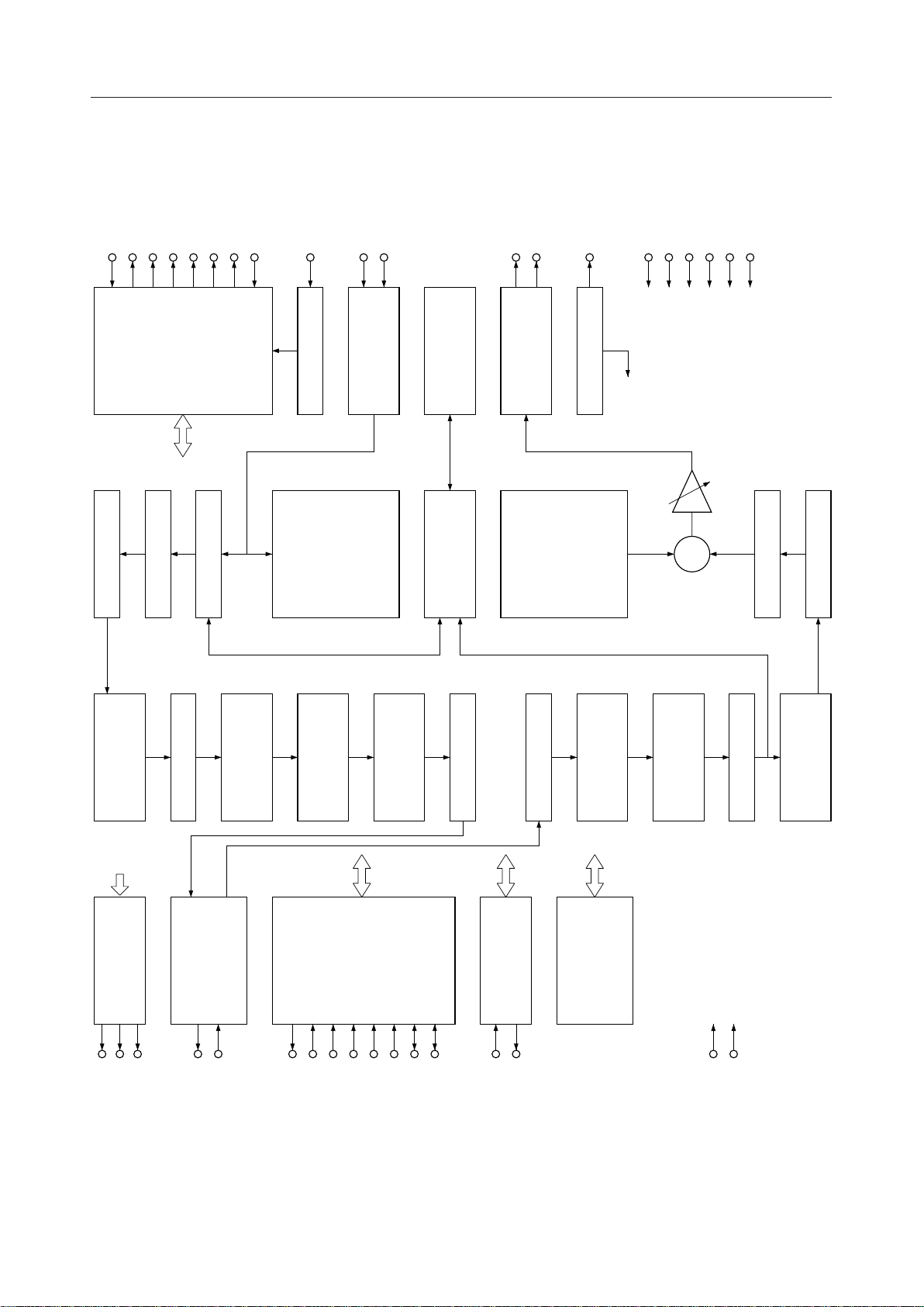
BLOCK DIAGRAM
1 - 5
A
ST1
ST2RTRBTM
SBTM
CPUCLK
GACLK
CKOEN
MCK
AINP
AINN
AOUTP
AOUTN
SG
DD
V
GND1 - 5
DD
V
P
DD
GNDA
V
GNDP
Clock
AGC
Demodulator
Filter
Roll Off
Generator
Filter
Equalizer
PLL
Carrier
Tone
Detector
PLL
(Answer)
Viterbi
Decorder
ADC
(DTMF)
(Calling)
(Program)
Decoder
Differential
Bulk
Delay RAM
Echo
Canceler
Descrambler
DAC
Tone
Generator
Scrambler
VREF
(DTMF)
(Guard)
(Answer)
Differential
(Program)
Encoder
+
Trellis
Encoder
Atten
Mapping
Filter
Modulator
Filter
Roll Off
2
Eye
XYCK
SOM
Monitor
SYCR
I/F
Serial
SRD
STD
STCHG
CPUTYPE
Parallel
CS0, 1
ALEWRRD
I/F
ADA7 - 0
AOD7 - 0
I/F
Test
TI0 - 9, BTD
TO0 - 13, BRD
Test
Circuit
V54 & V22
RST
SLEEP
Page 3
¡ Semiconductor MSM7564-01
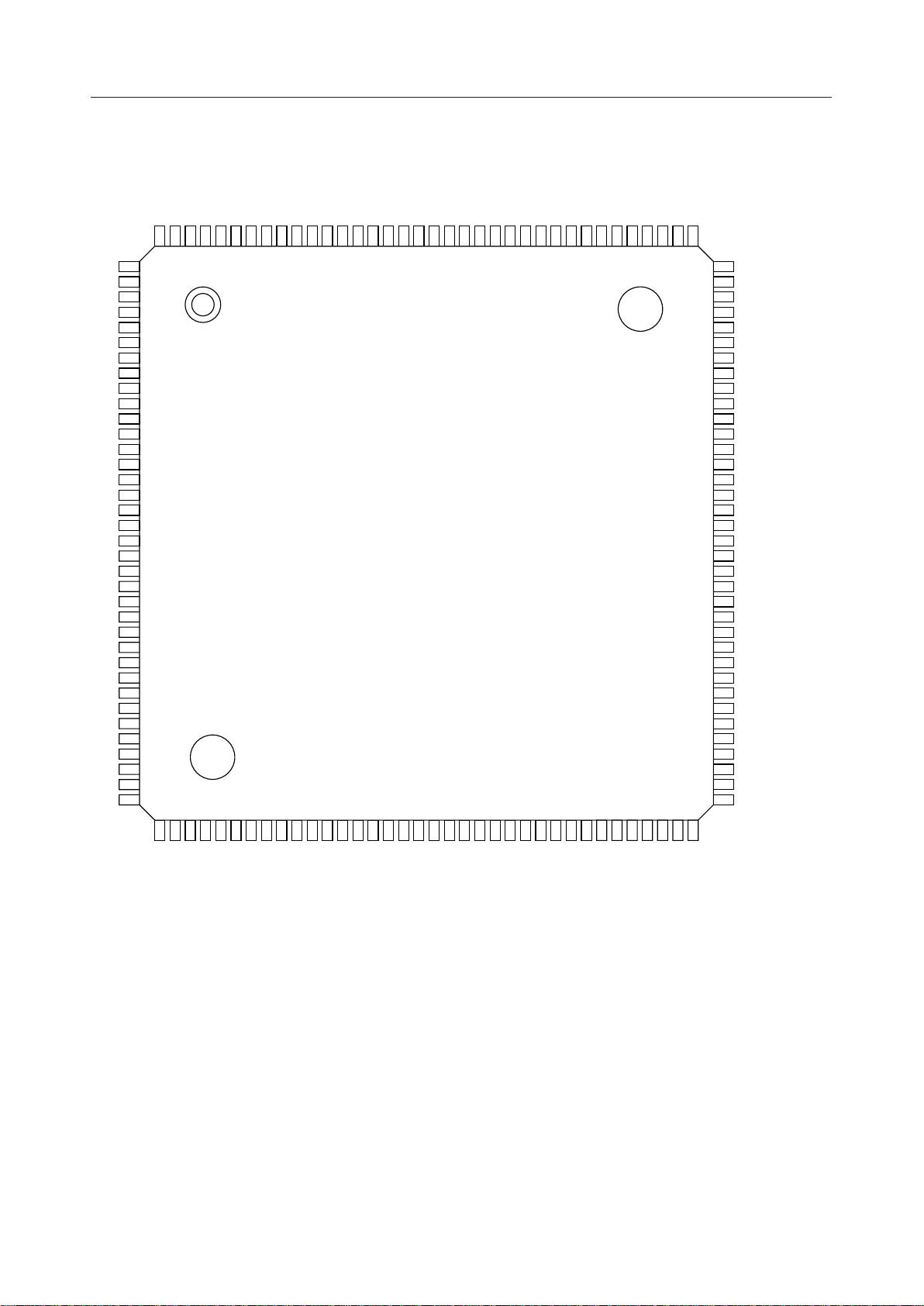
PIN CONFIGURATION (TOP VIEW)
144
143
142
141
140
139
138
137
136
135
134
133
132
131
130
129
128
127
126
125
124
123
122
121
120
119
118
117
116
115
114
113
112
111
110
109
1
2
3
4
5
6
7
8
9
10
11
12
13
14
15
16
17
18
19
20
21
22
23
24
25
26
27
28
29
30
31
32
33
34
35
36
108
107
106
105
104
103
102
101
100
99
98
97
96
95
94
93
92
91
90
89
88
87
86
85
84
83
82
81
80
79
78
77
76
75
74
73
3738394041424344454647484950515253545556575859606162636465666768697071
144-Pin Plastic TQFP
72
3
Page 4
MSM7564-01 ¡ Semiconductor
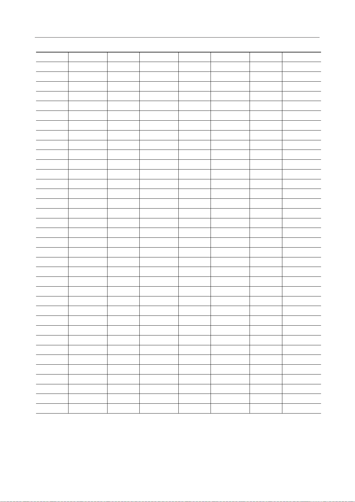
Pin Symbol
1 AINN
2NC
3 AINP
4 AOUTN
5NC
6NC
7 AOUTP
8V
DD
A
9 GND1
10 NC
11 TI2
12 NC
13 STD
14 NC
15 V
DD
1
16 NC
17 ST1
18 NC
19 WR
20 NC
21 BTD
22 NC
23 RD
24 NC
25 CS1
26 GND2
27 NC
28 RST
29 NC
30 CS0
31 NC
32 CKOEN
33 NC
34 SBTM
35 SLEEP
36 RBTM
Pin Symbol
37 NC
38 NC
39 TI4
40 TI3
41 NC
42 TI5
43 NC
44 TO4
45 NC
46 CPUTYPE
47 GND3
48 NC
49 BRD
50 ALE
51 NC
52 SOM
53 NC
54 V
DD
2
55 SYCR
56 NC
57 ST2
58 NC
59 XYCK
60 NC
61 SRD
62 STCHG
63 NC
64 TO2
65 NC
66 TO0
67 TO3
68 RT
69 NC
70 CPUCLK
71 GACLK
72 NC
Pin Symbol
73 TO1
74 ADA6
75 ADA4
76 ADA3
77 V
DD
3
78 NC
79 ADA2
80 NC
81 ADA0
82 NC
83 AOD7
84 NC
85 AOD6
86 NC
87 NC
88 AOD5
89 NC
90 GND4
91 NC
92 AOD4
93 NC
94 AOD3
95 NC
96 AOD2
97 NC
98 NC
99 AOD1
100 NC
101 V
DD
4
102 AOD0
103 ADA5
104 NC
105 NC
106 ADA1
107 ADA7
108 TI8
Pin Symbol
109 NC
110 TO10
111 TO6
112 NC
113 TO13
114 TO12
115 NC
116 TO11
117 TO7
118 NC
119 TO9
120 NC
121 TO8
122 NC
123 TI6
124 TI7
125 NC
126 V
DD
5
127 TI1
128 NC
129 TI0
130 NC
131 TI9
132 GND5
133 V
DD
P
134 MCK
135 NC
136 NC
137 TO5
138 GNDP
139 GNDA
140 NC
141 NC
142 NC
143 SG
144 NC
NC : No connect pin
4
Page 5
¡ Semiconductor MSM7564-01
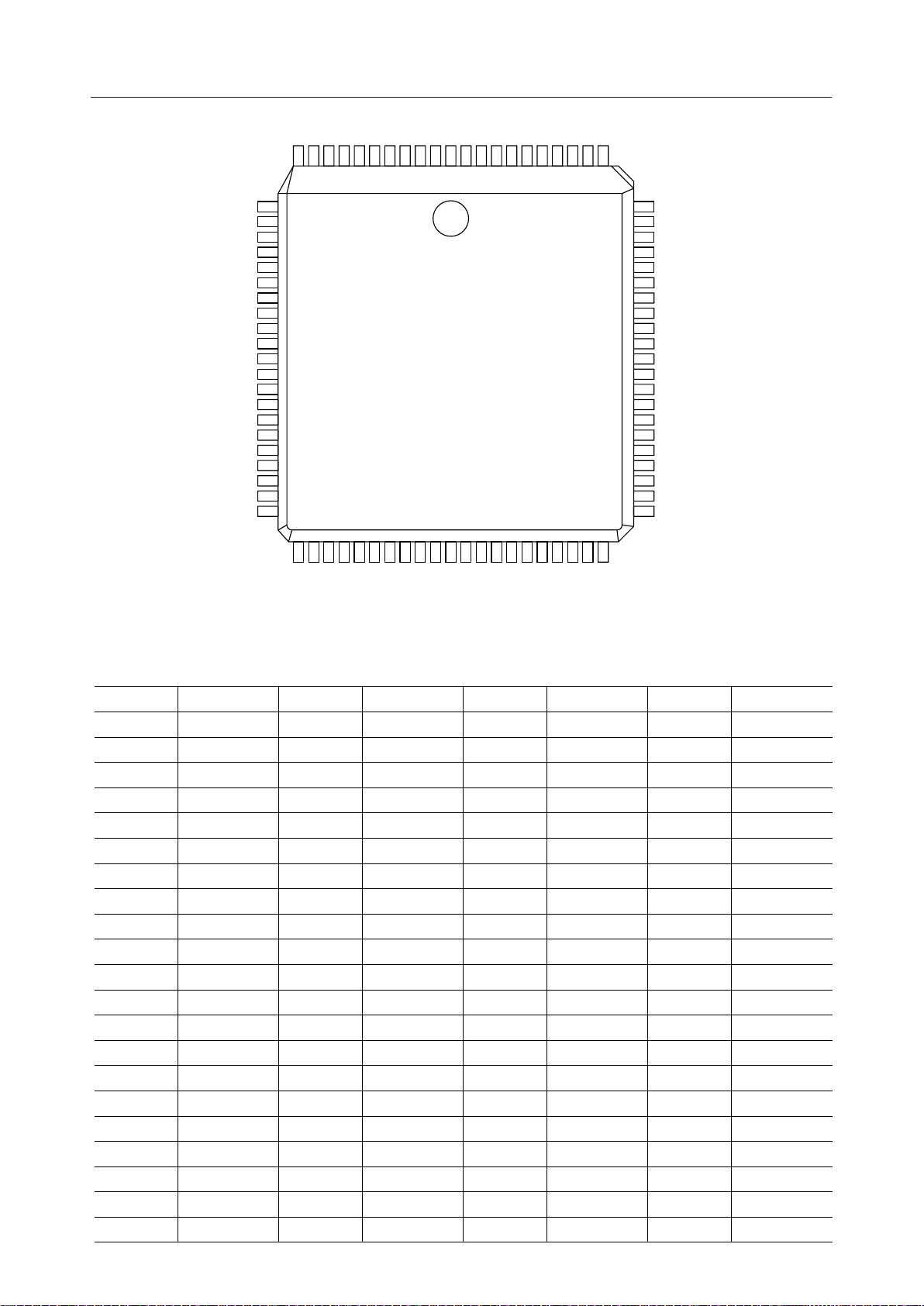
987654321
11
10
848382818079787776
75
12
13
14
15
16
17
18
19
20
21
22
23
24
25
26
27
28
29
30
31
32
333435363738394041424344454647484950515253
84-Pin Plastic QFJ
74
73
72
71
70
69
68
67
66
65
64
63
62
61
60
59
58
57
56
55
54
Pin Symbol
1 GND4
2 AOD4
3 AOD3
4 AOD2
5 AOD1
6V
DD
4
7 AOD0
8ADA5
9ADA1
10 ADA7
11 TI8
12 TO10
13 TO6
14 TO13
15 TO12
16 TO11
17 TO7
18 TO9
19 TO8
20 TI6
21 TI7
Pin Symbol
22 V
DD
5
23 TI1
24 TI0
25 TI9
26 GND5
27 V
DD
P
28 MCK
29 TO5
30 GNDP
31 GNDA
32 SG
33 AINN
34 AINP
35 AOUTN
36 AOUTP
37 V
DD
A
38 GND1
39 TI2
40 STD
41 V
DD
1
42 ST1
Pin Symbol
43 WR
44 BTD
45 RD
46 CS1
47 GND2
48 RST
49 CS0
50 CKOEN
51 SBTM
52 SLEEP
53 RBTM
54 TI4
55 TI3
56 TI5
57 TO4
58 CPUTYPE
59 GND3
60 BRD
61 ALE
62 SOM
63 V
DD
2
Pin Symbol
64 SYCR
65 ST2
66 XYCK
67 SRD
68 STCHG
69 TO2
70 TO0
71 TO3
72 RT
73 CPUCLK
74 GACLK
75 TO1
76 ADA6
77 ADA4
78 ADA3
79 V
DD
3
80 ADA2
81 ADA0
82 AOD7
83 AOD6
84 AOD5
5
Page 6
MSM7564-01 ¡ Semiconductor
PIN DESCRIPTIONS
System and Clock
Symbol
MCK
RST
SLEEP
CKOEN
CPUCLK
GACLK
Type
I
I
I
I
O
O
Master Clock Input
Frequency of 3.888 MHz ±100 ppm, with a duty ratio of between 45 and 55%.
Reset Input
'0' : reset state, '1' : normal operation
Sleep Input
'0' : sleep state, '1' : normal operation
Clock Output Enable
'0' : CPUCLK and GACLK pins are enabled to output.
(Internal PLL operates normally in sleep state.)
'1' : CPUCLK and GACLK pins are disabled to output.
(Internal PLL turns to be power down in sleep state.)
CPU Clock Output
CPUCLK outputs a 15.552 MHz clock for external CPU.
Gate Array Clock Output
GACLK outputs a 13.824 MHz clock for external gate array.
Modem Digital Interface
Description
Symbol
ST1
ST2
RT
STD
SRD
Type
I
O
O
I
O
Description
External Transmit Clock Input
An external transmit clock provided to input to ST1. The clock frequency of 300 to
14400 Hz is supplied by the local DTE.
Internal Transmit Clock Output
ST2 outputs the transmitting data clock of between 300 and 14400 Hz selected by
modem mode.
Internal Receive Clock Output
RT outputs the receiving data clock of between 300 and 14400 Hz selected by modem
mode.
Transmit Data Serial Input
STD inputs the transmit serial data synchronized with either internal timing selected by
modem mode or ST1 / ST2.
Received Data Serial Output
SRD outputs the received serial data synchronized with either internal timing selected
by modem mode or RT.
6
Page 7

¡ Semiconductor MSM7564-01
CPU Interfaces
Symbol
CPUTYPE
STCHG
CS0, 1
ALE
RD
WR I
ADA7 - 0 I/O
AOD7 - 0 I/O
Type
O
CPU Type Select
I
CPUTYPE selects CPU bus type of ADA7 - 0 and AOD7 - 0.
'1' : 80 mode (multiplexed address and data bus for Intel-compatible)
'0' : 68 mode (separated address and data bus for Motorola-compatible)
Status Change Output
When interface memory registers (0C, 0D, 1E, 1F) change, STCHG is set to "0". When
the registers are read by external CPU, this pin is set to '1'.
Chip Select Input 0 and 1
I
When CS0 and CS1 are set to '1', this chip is selected for microprocessor operation.
Address Latch Enable Input
I
ALE allows the microprocessor to latch the address bus (ADA7 - 0) when CPUTYPE is
80 mode. Address bus is latched at the falling edge of ALE.
Read Enable
I
RD is active LOW and is used to read from internal memory register via 8-bit address
data input/output pins selected by CPUTYPE pin. CS0 and CS1 must be high.
Write Enable
WR is active Low and is used to write the data at the rising edge via data input/output
pins selected by CPUTYPE pin into internal memory registers. CS0 and CS1 must be
high.
8 bit Address and Data Bus 1
8 lines provide 2 modes of bus type which are selected by CPUTYPE pin. AD7 to 0 are
controlled by ALE, RD and WR.
80 mode : (I/O) address input and data input/output
68 mode : (I) address input
8 bit Address and Data Bus 2
8 lines provide 2 modes of bus type which are selected by CPUTYPE pin. AD7 to 0 are
controlled by ALE, RD and WR.
80 mode : (O) address output (outputs latched address by ALE)
68 mode : (I/O) address input/output
Description
7
Page 8
MSM7564-01 ¡ Semiconductor
Other Interfaces
Symbol
RBTM
SBTM
SOM
XYCK
SYCR O
Type
Receive Baud Rate Timing Clock Output
O
RBTM outputs receive baud rate timing clock of between 600 and 2400 Hz selected by
modem mode.
Transmit Baud Rate Timing Clock Output
O
RBTM outputs transmit baud rate timing clock of between 600 and 2400 Hz selected
by modem mode.
Serial Eye Pattern X/Y Output
O
SOM outputs serial pattern containing two 16 bit words (X, Y references), synchronized
with the falling edge of XYCK.
Serial Eye Pattern Clock Output
O
XYCK outputs a 1152 Hz clock for SOM timing.
Serial Eye Pattern Timing Output
SYCR outputs synchronous timing for SOM output.
SYCR outputs two clocks of SOM clocks.
Description
8
Page 9
¡ Semiconductor MSM7564-01
Test Interface
Symbol Type Description
TI0 I TEST PIN. Connect to ground.
TI1 I TEST PIN. Connect to ground.
TI2 - 4 I TEST PIN. Connect to ground.
TI5, 6 I TEST PIN. Connect to ground.
TI7 I TEST PIN. Connect to ground.
TI8 I TEST PIN. Connect to ground.
TI9 I TEST PIN. Connect to V
BTD I TEST PIN. Connect to V
TO0 I/O TEST PIN. Leave "OPEN".
TO1 I/O TEST PIN. Leave "OPEN".
TO2 I/O TEST PIN. Leave "OPEN".
TO3 I/O TEST PIN. Connect to ground.
TO4 I/O TEST PIN. Leave "OPEN".
TO5 O TEST PIN. Leave "OPEN".
TO6 - 13 I/O TEST PIN. Leave "OPEN".
BRD O TEST PIN. Leave "OPEN".
DD
DD
.
.
Analog Interface
Symbol
AINP
AINN
AOUTP
AOUTN
SG
Type
O
O
O
Power Supply
Symbol
1 - 5
V
DD
GND1 - 5
P
V
DD
GNDP
V
A
DD
GNDA
Type
Description
I
Analog Input (positive)
I
Analog Input (negative)
Analog Output (positive)
AOUTP is in high impedance state when CKOEN is '1' state and in sleep mode.
Analog Output (negative)
AOUTN is in high impedance state when CKOEN is in '1' state and in sleep mode.
Signal Ground for Analog
The SG level is about +2.4 V. Connect bypass capacitor between SG and GNDA when
CKOEN is in '1' state and in sleep mode.
Description
DD
DD
.
DD
.
.
I
Digital V
Digital Ground.
I
PLL V
I
PLL Ground.
I
Analog V
I
I
Analog Ground.
9
Page 10

MSM7564-01 ¡ Semiconductor
FUNCTIONAL DESCRIPTION
Modem Mode
MSM7564 conforms to ITU-T Recommendation and Bell standard as follows.
Modem Mode Data Rate
(bps) (Hz)
V.17 14400 TCM 1800 2400 sync
V.17 12000 TCM 1800 2400 sync
V.17 9600 TCM 1800 2400 sync
V.17 7200 TCM 1800 2400 sync
V.32bis 14400 TCM 1800 2400 sync/async
V.32bis 12000 TCM 1800 2400 sync/async
V.32bis 9600 TCM 1800 2400 sync/async
V.32bis 7200 TCM 1800 2400 sync/async
V.32 9600 QAM 1800 2400 sync/async
V.32 4800 QAM 1800 2400 sync/async
V.29 9600 QAM 1700 2400 sync
V.29 7200 QAM 1700 2400 sync
V.29 4800 PSK 1700 2400 sync
V.27ter 4800 PSK 1800 1600 sync
V.27ter 2400 PSK 1800 1200 sync
V.22bis 2400 QAM 1200/2400 600 sync/async
V.22 1200 PSK 1200/2400 600 sync/async
Bell212A 1200 PSK 1200/2400 600 sync/async
V.21 300 FSK 1080/1750 300 async
V.21ch2 300 FSK 1080/1750 300 sync
Bell103 300 FSK 1170/2125 300 async
Modulation
Carrier Frequency Baud Rate Synchronous/
Asynchronous
Note
Backward Channel ON/OFF
Backward Channel ON/OFF
10
Page 11

¡ Semiconductor MSM7564-01
Serial Interface
MSM7564 provides a one channel serial interface, including synchronous-asynchronous and
asynchronous-synchronous converters. Select synchronous or asynchronous. In synchronous mode,
the transmit data is synchronized with the clock provided from this chip or DTE. Serial transmit data
to STD pin is latched with the rising edge of ST1 or ST2, and receive data on SRD is output
synchronously with the falling edge of RT. This chip also includes a scrambler and descrambler.
Parallel Interface
MSM7564 contains twenty 8-bit registers (location from addresses 00H through 0FH and 1C through
1F), which are used to control this chip and to detect various signals. Connect this chip to either
multiplexed address and data bus such as Intel-compatible (80 mode) or separate address and data
bus such as Motorola-compatible (68 mode).
Transmit and Receive Level
Analog input and output are differential amplifiers, and are ±1.2 V
peak signals. The level of the
O-P
transmit line signal is –10 dBm. The modem can provide 15 dB programmable transmit attenuation
with 1 dB steps controlled by the TXLEV bit in located 0BH register. Receive signal level is from –10
dBm to –43 dBm. Carrier detection level can be selected from 4 levels (–43, –33, –26, –16 dBm) by the
CDLEV bit located in register 0BH. An amplitude equalizer in transmitter and receiver can be
individually controlled by RAEQL and SAEQL bits in register 07H.
DTMF Tone, Answer Tone, and Guard Tone Generators
The modem can generate 16 types of DTMF tones using the PBANSEL bit located in register 05H.
It also generates answer tone and guard tone.
Various Detection Circuits
The internal detection circuit monitors carrier, call progress tone, answer tone, DTMF tone, and other
receive signals needed for each modem mode, and stores them in the corresponding bits of each of
the following registers : 0C, 0D, 1C, and 1D. Classification of detected tones is controlled by
DETMODE bit in register 08H. If the contents of registers 0C, 0D, 1C, and 1D change, the interruption
signal (STCHG) for controlling microprocessor is generated.
Programmable Tone Generator and Detector
The transmission of programmable tone 1 and tone 2 is available and is controlled by PTONE1 and
PTONE2 bits in 05H register. To use this function, the initial download of frequency and gain is
needed. This modem can output 16 kinds of frequency selected by PBANSEL bit of register 05H
(composition of two tones is also available.). PTONE1 and PTONE2 are the same frequency and only
the gain is variable. Each bit of D7, D6, D3, D2, D1, and D0 in register 0C can be used for
programmable tone detecting by rewriting a coefficient of internal filter at the initial download.
11
Page 12

MSM7564-01 ¡ Semiconductor
Received Signal Quality Monitor
The modem indicates a state of received signal quality using the SQD bit of register 0D. If this bit
changes, an interrupt signal (STCHG) for controlling the microprocessor is generated. Furthermore,
it can read the bit error rate and receive level (stored in internal RAM) required for MNP class 10.
Echo Canceler
The modem has internal RAM for bulk delay and can cope with delays of up to 1.2 s for far-end echo.
Voice Output Function
The voice output is enabled by setting MODEMSET bit of register 06 to voice mode. In this case, voice
data of 7.2 kHz sampling of 8 bits must be written in 00, 01, and 02 registers with the rising edge of
RBTM (2.4 kHz).
Test Mode
The modem performs the internal local analog loop testing by the LALTST bit of register 07H. It also
performs external local analog loop testing by the LALTST bit of register 07H and by connecting
transmit analog output and receive analog input. Remote digital loop is available by the LOOP2 bit
of register 1EH.
It can output a 511PN pattern and 1 to 1 pattern for error test controlling PN511 and ERR11 bits of
register 1EH.
Error counts can be read controlling ERRCNT bit of register 1DH.
Sleep Mode
The modem supports a sleep function by controlling SLEEP bit of register 04H and SLEEP pin. It
provides two modes of sleep1 (clock generator is inactive at CKOEN = '1') and sleep2 (clock generator
is active at CKOEN = '0') controlled by CKOEN pin. Cancellation of sleep mode is controlled by
SOFTRST bit of register 04H and RST pin.
12
Page 13

¡ Semiconductor MSM7564-01
Control register
The modem contains twenty 8-bit registers for control and signal detection monitoring. These
registers are assigned by the address (ADA7-0 or AOD7-0) as shown in the following table.
• Table of control register
REG (H) D7 D6 D5 D4 D3 D2 D1 D0
1F W SB1DEN RDZ SDZ SDA WSIZE EXTEND ASYN
1E W TXCLK ERR11 PN511 SB11 PN1 PN0 LOOP2
1D R
1C R
0F W write "0"
0E R DON'T CARE DCD CTS
VOICE PBTONE NO
0D R
0C R V32 1650 1300
V22ORG 2225 1100
V22ANS 980 1100
V21ORG 1650 1300
V21ANS 980 1300
Bell103ORG 2225 1300
Bell103ANS 1270 1300
V17, V21ch2 1650 1300 1750 3000 AC 1800 AA 600 AC
VOICE 1100 1300
0B W
0A W ILDCNT DSPST write "0" write "0" STRN BRTS EPT RTS
09 W V32 EB1 RATES TRN ECTRN SS XCHG AACC ACCA
VOICE write "0" VSMODE write "0"
08 W DETMODE AQID TIMC TANI JHOLD EHOLD TAPH
07 W LALTST GTS GTE RAEQL SAEQL
VOICE write "0" VEN RAEQL SAEQL
06 W MODEMSET
05 W PBANSEL SFIL PBANS PTONE2 PTONE1
04 W write "0" NEGO STUP AUTO EQLST SLEEP
DON'T CARE
DON'T CARE DON'T CARE DON'T CARE DON'T CARE
DON'T CARE
V29 1650 1300 1750 2900 1700 500
V27 1650 1300 1750 2600 1800 1000
AGCRST
V22 write "0" write "0" write "0" SB124 SB112 USB124 USB112 S1
BRKDET ERRCNT
USB124D USB112D
DSPRST PBDET TRN FCD SQD EED RATED
2250USB1
2250USB1
1270USB1
2250USB1
2250USB1
CPGDET
AGCH TXLEV CDLEV
ANSDET
2250USB1
2250USB1
2250USB1
SB11DET
3000 AC 1800 AA 600 AC
2700 S1 2400 S1 2100 S1
1500 S1 1200 S1 900 S1
3000 AC 1800 AA 600 AC
3000 AC 1800 AA 600 AC
3000 AC 1800 AA 600 AC
3000 AC 1800 AA 600 AC
3000 AC 1800 AA 600 AC
PN1DET PN0DET
SB124D SB112D
ORGANS
ORGANS
SOFTRST
V32DATA
write "0"
RAMRDWR
13
Page 14

MSM7564-01 ¡ Semiconductor
• Table of control register (Continued)
REG (H) D7 D6 D5 D4 D3 D2 D1 D0
03 R/W DRAMDH (F-8)
VOICE write "0" VSEN write "0" write "0" VIOF write "0"
02 R/W DRAMDL (7-0)
VOICE VDATA3RD
01 R/W DRAMAH (F-8)
VOICE VDATA2ND
00 R/W DRAMAL(7-0)
VOICE VDATA1ST
Notes: 1. W:Write Only, R: Read Only, R/W: Read/Write.
2. Deal with the following modes due to MODEMSET bit of 06H register and ORGANS
bit of 07H register.
V32: V.32bis & V.32, V22: V.22bis & V.22, V21: V.21, V17: V.17, V21ch2: V.21ch2, V29:
V.29, V23: V.23, V27: V.27ter, VOICE: Voice mode, ORG: Originate, ANS: Answer
14
Page 15

¡ Semiconductor MSM7564-01
Control register functional summary
FUNCTIONSYMBOLBITREG (H)
00 R/W
01 R/W
02 R/W
03 R/W
00 R/W
(VOICE)
01R/W
(VOICE)
02 R/W
(VOICE)
03 R/W
(VOICE)
04 W
05 W
06 W
07 W
07 W
(VOICE)
7-0
7-0
7-0
7-0
7-0
7-0
7-0
1
4
0
1
2
3
4
5
6
0
1
2
3
7-4
7-0
0
1
2
3
4
5
7-6
1
2
3
4
DRAMAL (7-0)
DRAMAH (F-8)
DRAMDL (7-0)
DRAMDH (F-8)
VDATA1ST
VDATA2ND
VDATA3RD
VIOF
VSEN
RAMRDWR
SOFTRST
SLEEP
EQLST
AUTO
STUP
NEGO
PTONE1
PTONE2
PBANS
SFIL
PBANSEL
MODEMSET
V32DATA
ORGANS
SAEQL
RAEQL
GTE
GTS
LALTST
ORGANS
SAEQL
RAEQL
VEN
Specify low-order 8-bit (bit7 - 0) of the address to access an internal RAM.
Specify high-order 8 bits (bit15 - 8) of the address to access an internal RAM.
Store low-order 8 bits of the data to access an internal RAM.
Store high-order 8 bits of the data to access an internal RAM.
Voice output 1st data
Voice output 2nd data
Voice output 3rd data
Input/output flag of voice data output
Enables voice data output.
When internal RAM is accessed, selects read or write.
Soft reset
Sleep
Controls adaptive equalizer.
Specifies control method of adaptive equalizer.
Start-up control
Auto negotiation control
Programmable tone control 1
Programmable tone control 2
PB tone and answer tone control
Transmission filter control
Selects PB tone and answer tone.
Modem mode setting.
Selects V.32bis and V.32 operating mode.
Sets originate mode and answer mode.
Sets adaptive equalization for transmit.
Sets adaptive equalization for receive.
Sets guard tone generator.
Sets guard tone frequency.
Local analog loop back test control
Sets originate mode and answer mode.
Sets transmit amplitude equalizer.
Sets receive amplitude equalizer.
Enables voice output.
15
Page 16

MSM7564-01 ¡ Semiconductor
Control register functional summary (Continued)
FUNCTIONSYMBOLBITREG (H)
08 W
09 W
(V22)
09 W
(V32)
09 W
(VOICE)
0A W
0B W
0C W
(V32)
0
1
2
3
4
5
7-6
0
1
2
3
4
0
1
2
3
4
5
6
7
6-4
0
1
2
3
6
7
1-0
5-2
6
7
0
1
2
3
4
5
6
7
TAPH
EHOLD
JHOLD
TANI
TIMC
AQID
DETMODE
S1
USB112
USB124
SB112
SB124
ACCA
AACC
XCHG
SS
ECTRN
TRN
RATES
EB1
VSMODE
RTS
EPT
BRTS
STRN
DSPST
ILDCNT
CDLEV
TXLEV
AGCH
AGCRST
600 AC
1800 AA
3000 AC
2250USB1
ANSDET
CPGDET
1300
1650
Holds automatic equalizer, jitter canceler, and carrier PLL.
Holds automatic equalizer and jitter canceler.
Holds jitter canceler.
Uses automatic equalizer of unit taps.
A pass through timing PLL
Clears automatic equalizer, jitter canceler, and carrier PLL.
Sets tone detection mode.
Transmits S1 signal.
Transmits unscrambled binary 1 at 1200 bps.
Transmits unscrambled binary 1 at 2400 bps.
Transmits scrambled binary 1 at 1200 bps.
Transmits scrambled binary 1 at 2400 bps.
Transmits signals AC and CA.
Transmits signals AA and CC.
Selects signals AA and CC. Exchage command of AA/CC
Transmits signal S.
Transmits echo canceler training signal.
Transmits consecutive signals S, S, and TRN.
Transmits signals R1 to R3.
Transmits consecutive signals E and B1
Controls coding method at voice output.
Request of transmission.
Transmits echo protector tone.
Sets RTS of backward channel.
Selects short or long training.
DSP start
Initial load control
Carrier Detect Threshold Level select.
Set programmable attenuator for transmission.
AGC hold
AGC reset
Detects signal AC of 600 Hz.
Detects signal AA of 1800 Hz.
Detects signal AC of 3000 Hz.
Detects unscrambled binary 1 at 2250 Hz.
Detects answer tone.
Detects call progress tone.
Detects signal of 1300 Hz.
Detects signal of 1650 Hz.
16
Page 17

¡ Semiconductor MSM7564-01
Control register functional summary (Continued)
FUNCTIONSYMBOLBITREG (H)
0C W
(V22ORG)
0C W
(V22ANS)
0C W
(V21ORG)
0C W
(V21ANS)
0C W
(Bell 103 ORG)
0
1
2
3
4
5
6
7
0
1
2
3
4
5
6
7
0
1
2
3
4
5
6
7
0
1
2
3
4
5
6
7
0
1
2
3
4
5
6
7
2100 S1
2400 S1
2700 S1
2250USB1
ANSDET
CPGDET
1100
2225
900 S1
1200 S1
1500 S1
1270USB1
ANSDET
CPGDET
1100
980
600 AC
1800 AA
3000 AC
2250USB1
ANSDET
CPGDET
1300
1650
600 AC
1800 AA
3000 AC
2250USB1
ANSDET
CPGDET
1300
980
600 AC
1800 AA
3000 AC
2250USB1
ANSDET
CPGDET
1300
2225
Detects signal S1 of 2100 Hz.
Detects signal S1 of 2400 Hz.
Detects signal S1 of 2700 Hz.
Detects unscrambled binary 1 at 2250 Hz.
Detects answer tone.
Detects call progress tone.
Detects signal of 1100 Hz.
Detects signal of 2225 Hz.
Detects signal S1 of 900 Hz.
Detects signal S1 of 1200 Hz.
Detects signal S1 of 1500 Hz.
Detects unscrambled binary 1 at 1270 Hz.
Detects answer tone.
Detects call progress tone.
Detects signal of 1100 Hz.
Detects signal of 980 Hz.
Detects signal AC of 600 Hz.
Detects signal AA of 1800 Hz.
Detects signal AC of 3000 Hz.
Detects unscrambled binary 1 at 2250 Hz.
Detects answer tone.
Detects call progress tone.
Detects signal of 1300 Hz.
Detects signal of 1650 Hz.
Detects signal AC of 600 Hz.
Detects signal AA of 1800 Hz.
Detects signal AC of 3000 Hz.
Detects unscrambled binary 1 at 2250 Hz.
Detects answer tone.
Detects call progress tone.
Detects signal of 1300 Hz.
Detects signal of 980 Hz.
Detects signal AC of 600 Hz.
Detects signal AA of 1800 Hz.
Detects signal AC of 3000 Hz.
Detects unscrambled binary 1 at 2250 Hz.
Detects answer tone.
Detects call progress tone.
Detects signal of 1300 Hz.
Detects signal of 2225 Hz.
17
Page 18

MSM7564-01 ¡ Semiconductor
Control register functional summary (Continued)
FUNCTIONSYMBOLBITREG (H)
0C W
(Bell 103 ANS)
0C W
(V17, V21ch2)
0C R
(V29)
0C R
(V27)
0C W
(VOICE)
0
1
2
3
4
5
6
7
0
1
2
3
4
5
6
7
0
1
2
3
4
5
6
7
0
1
2
3
4
5
6
7
0
1
2
3
4
5
6
7
600 AC
1800 AA
3000 AC
2250USB1
ANSDET
CPGDET
1300
1270
600 AC
1800 AA
3000 AC
1750
ANSDET
CPGDET
1300
1650
500
1700
2900
1750
ANSDET
CPGDET
1300
1650
1000
1800
2600
1750
ANSDET
CPGDET
1300
1650
600 AC
1800 AA
3000 AC
2250USB1
ANSDET
CPGDET
1300
1100
Detects signal AC of 600 Hz.
Detects signal AA of 1800 Hz.
Detects signal AC of 3000 Hz.
Detects unscrambled binary 1 at 2250 Hz.
Detects answer tone.
Detects call progress tone.
Detects signal of 1300 Hz.
Detects signal of 1270 Hz.
Detects signal AC of 600 Hz.
Detects signal AA of 1800 Hz.
Detects signal AC of 3000 Hz.
Detects signal of 1750 Hz.
Detects answer tone.
Detects call progress tone.
Detects signal of 1300 Hz.
Detects signal of 1650 Hz.
Detects signal of 500 Hz.
Detects signal of 1750 Hz.
Detects signal of 2900 Hz.
Detects signal of 1750 Hz.
Detects answer tone.
Detects call progress tone.
Detects signal of 1300 Hz.
Detects signal of 1650 Hz.
Detects signal of 1000 Hz.
Detects signal of 1800 Hz.
Detects signal of 2600 Hz.
Detects signal of 1750 Hz.
Detects answer tone.
Detects call progress tone.
Detects signal of 1300 Hz.
Detects signal of 1650 Hz.
Detects signal AC of 600 Hz.
Detects signal AA of 1800 Hz.
Detects signal AC of 3000 Hz.
Detects unscrambled binary 1 at 2250 Hz.
Detects answer tone.
Detects call progress tone.
Detects signal of 1300 Hz.
Detects signal of 1100 Hz.
18
Page 19

¡ Semiconductor MSM7564-01
Control register functional summary (Continued)
FUNCTIONSYMBOLBITREG (H)
0D R
0E R
0E R
(VOICE)
1C R
1D R
1E W
1F W
0
1
2
3
4
5
6
0
1
0
0
1
2
3
0
1
2
5-3
6
0
1
2
3
4
5
7-6
0
1
3-2
4
5
6
7
RATED
EED
SQD
FCD
TRN
PBDET
DSPRST
CTS
DCD
PBTONE NO
SB112D
SB124D
USB112D
USB124D
PN0DET
PN1DET
SB11DET
ERRCNT
BRKDET
LOOP2
PN0
PN1
SB11
PN511
ERR11
TXCLK
ASYN
EXTEND
WSIZE
SDA
SDZ
RDZ
SB1DEN
Detects rate signal.
Detects end signal.
Indicates a state of received signal quality.
Detects fast carrier.
Indicates a state of training.
Detects PB tone.
DSP reset
Ready for sending.
Detects carrier
PB tone number
Detects scrambled binary 1 at 1200 bps.
Detects scrambled binary 1 at 2400 bps.
Detects unscrambled binary 1 at 1200 bps.
Detects unscrambled binary 1 at 2400 bps.
Detects preparatory signal.
Detects answer / termination signal.
Detects SB11
Error Count
Detects break signal.
Controls Loop2 test.
Transmits preparatory signal.
Transmits answer /termination signal.
Transmits SB11
Transmits signal 511PN for error test.
Transmits 1 to 1 signal for error test.
Sets transmitter signal element timing.
Selects synchronous or asynchronous.
Sets extended asynchronous mode.
Sets a character size for synchronous to asynchronous converter.
Transmitted data clamped to A
Transmitted data clamped to Z
Received data clamped to Z
Controls detection of scrambled binary 1.
19
Page 20

MSM7564-01 ¡ Semiconductor
ABSOLUTE MAXIMUM RATINGS
Parameter
Power Supply Voltage
Analog Input Voltage
Digital Input Voltage
Digital Output Voltage
Storage Temperature
Symbol
V
DD
V
AIN
V
DIN
V
OUT
T
STG
Rating
–0.3 to V
–0.3 to V
–0.3 to V
–0.3 to V
–55 to + 150
RECOMMENDED OPERATING CONDITIONS
Parameter
Power Supply Voltage
Operating Temperature
Symbol
V
DD
T
op
Min.
4.75
–20
Typ.
5.00
RECOMMENDED OPERATING CONDITIONS (ANALOG)
Parameter
Input Impedance
Output Load Impedance
Output Load Capacitance
Analog Input Amplitude
SG Output Voltage
Symbol
R
AI
R
AOL
C
AOL
V
AIN
V
SG
Min.
50
20
—
—
2.35
Typ.
2.40
—
—
—
—
—
DD
DD
DD
DD
+ 0.3
+ 0.3
+ 0.3
+ 0.3
Max.
5.25
70
Max.
—
—
100
V
SG
2.45
Unit
V
V
V
V
°C
Unit
V
°C
Unit
kW
kW
pF
V
PP
V
20
Page 21

¡ Semiconductor MSM7564-01
ELECTRICAL CHARACTERISTICS
DC Characteristics
Parameter Symbol Typ. UnitMin. Max.Condition
Input Leakage Current
Output Leakage Current
High-level Input Voltage *1
High-level Input Voltage *2
Low-level Input Voltage *1
Low-level Input Voltage *2 V
High-level Output Voltage *1 V
High-level Output Voltage *2 V
Low-level Output Voltage *1 V
Low-level Output Voltage *2 V
Stand-by Current 1
(Sleep Mode)
Stand-by Current 2
(Sleep Mode)
Average Power Supply Current
(Operating)
I
I
LO
V
V
V
I
DDS1
I
DDS2
I
DDO
LI
IH
IH
IL
IL
OH
OH
OL
OL
VIN = VDD/0 V
V
= VDD/0 V
IN
clock generator inactive
state (CKOEN = 1)
clock generator active
state (CKOEN = 0)
MCK = 3.888 MHz
—
—
—
–10
–10
4.0
2.4
–0.3
–0.3 V—
4.2 VIOH = –400 mA
4.2 VIOH = –200 mA
—VIOL = 3.2 mA
—VIOL = 1.6 mA
—mA
—mA
—mA
—
—
—
—
—
—
—
—
—
—
—
35
100
10
10
V
+ 0.3
DD
+ 0.3
V
DD
0.8
0.8
—
—
0.4
0.4
2
—
—
mA
mA
V
V
V
Notes: *1: Applied to RST, SLEEP pins.
*2: Applied to input pins except those of *1.
*3: Applied to ADA7 - 0 and AOD7 - 0 pins.
*4: Applied to output pins except those of *3.
AC Characteristics (CPU Interface : 68 mode)
Parameter
Address and Chip Select Setup
Time (to WR Negative Edge)
Address and Chip Select Setup
Time (to WR Positive Edge)
WR Pulse Width
Data-in Setup Time t
Data-in Hold Time t
Address and Chip Select Setup
Time (to WR Negative Edge)
Address and Chip Select Setup
Time (to RD Positive Edge)
RD Pulse Width t
Data-out Delay Time
(to RD Negative Edge)
Data-out Hold Time
(to RD Positive Edge)
Symbol
t
CWS1
t
CWH1
t
WW1
DWS1
DWH1
t
CRS1
t
CRH1
RW1
t
DOD1
t
DOH1
Min.
30
15
45
Typ.
—
—
—
Max.
—
—
—
Unit
ns
ns
ns
—ns30 —
—ns15 —
—ns30 —
—ns15 —
—ns45 —
—ns—40
—ns0—
21
Page 22

MSM7564-01 ¡ Semiconductor
Write timing
ADA7 - 0
Address In
CS1, 0
t
CWS1
t
WW1
WR
AOD7 - 0 Data In
Read timing
ADA7 - 0
Address In
t
DWS1tDWH1
t
CWH1
CS1, 0
t
CRS1
t
RW1
RD
t
DOD1
AOD7 - 0 Data Out
t
DOH1
t
CRH1
22
Page 23

¡ Semiconductor MSM7564-01
AC Characteristics (CPU Interface : 80 mode)
Parameter
Symbol
ALE Pulse Width t
Address-in Setup Time t
Address-in Hold Time t
Chip Select Setup Time
(to WR Negative Edge)
Chip Select Hold Time
(to WR Positive Edge)
WR Pulse Width
Data-in Setup Time t
Data-in Hold Time t
Address-out Hold Time t
Address-out Delay Time t
Chip Select Setup Time
(to RD Negative Edge)
Chip Select Hold Time
(to RD Positive Edge)
RD Pulse Width t
Data-out Delay Time
(to RD Negative Edge)
Data-out Hold Time
(to RD Positive Edge)
AW2
AAS2
AAH2
t
CWS2
t
CWH2
t
WW2
DWS2
DWH2
AOH2
AOD2
t
CRS2
t
CRH2
RW2
t
DOD2
t
DOH2
Min.
30
15
45
Typ.
Max.
Unit
—ns30 —
—ns30 —
—ns15 —
—
—
—
—
—
—
ns
ns
ns
—ns30 —
—ns15 —
—ns0—
—ns—40
—ns30 —
—ns15 —
—ns45 —
—ns—40
—ns0—
23
Page 24

MSM7564-01 ¡ Semiconductor
Write timing
ALE
t
AW2
ADA7 - 0 Data In
t
AAS2
Address In
t
AAH2
CS1, 0
t
DWS2
WR
t
CWS2
AOD7 - 0
t
AOH2
t
AOD2
Address Out
Read timing
t
WW2
t
DWH2
t
CWH2
ALE
t
AW2
ADA7 - 0 Data Out
t
AAS2
Address In
t
AAH2
CS1, 0
t
DOD2
RD
AOD7 - 0
t
AOH2
t
AOD2
t
CRS2
Address Out
t
RW2
t
DOH2
t
CRH2
24
Page 25

¡ Semiconductor MSM7564-01
Analog Transmit Characteristics
Parameter
Transmit Carrier
Output level
(at TXLEV = 00)
Transmit signal
to noise ratio
DTMF Tone
Frequency
tolerance
Transmit level
(at TXLEV = 00)
Answer Tone
Frequency
tolerance
Transmit level
(at TXLEV = 00)
Analog Receive Characteristics
Parameter
Receive Carrier
Carrier Detector
Answer Tone
Call Progress Tone
Other Tone
Input level
Receive signal to
noise ratio
Detect level
Delay time
Hold time
Detect level
Delay time
Detect level
Symbol
TSFL
TSSN
Min.
–11.5
—
Typ.
–10
65
Max.
–8.5
—
Unit
dBm
dB
Note
–10 dBm output
F = 1209, 1336,
1477, 1633,
TSDF
F – 10
F
F + 10
Hz
697, 770,
852, 941 Hz
TSDLH
TSDLL
–7
–8.5
–5.5
–7
–4
–5.5
dBm
dBm
High channel
Low channel
F = 2100,
TSAF
F – 10
F
F + 10
Hz
2225 Hz
TSAL
Symbol
TRFL
–11.5
Min.
–43
–10
Typ.
—
–8.5
Max.
–10
dBm
Unit
dBm
Note
TRSN — 45 — dB –40 dBm input
CDDL
t
CDD
t
CDH
–48
—
—15—msHold time
—
25
–43
—
dBm
ms
ATDL –43 — — dBmDetect level
t
ATD
t
ATH
CTDL
t
CTD
OTDL
—25—msDelay time
—
–43
—
–43
25
—
50
—
—
—
—
—
dBm
dBm
2100 Hz / 2225 Hz
ms
350 to 620 Hz
ms
band
ex. DTMF tone
Note: A unit (dBm ) to signal power level is 600 W termination. 0 dBm is equal to 0.775 Vrms.
25
Page 26

MSM7564-01 ¡ Semiconductor
APPLICATION CIRCUITS
CPU Interface1
The modem supports an interface to connect directly to separate address-data bus such as a
Motorola-compatible CPU (68 mode : ex. Z80). The master clock (3.888 MHz) is assumed to be
supplied from an external crystal. The clock for Z80 or gate array clock generated in this device is sent
from CPUCLK and GACLK pins. The outline of connection is as follows.
Z80
A7 - A0
A15
A14
D7 - D0
RD
WR
INT1
CLK
crystal
3.888 MHz
MSM7564
MCK
ADA7 - ADA0
CS1
CS0
AOD7 - AOD0
RD
WR
ALE
GND
STCHG
CPUTYPE
CKOEN
GND
CPUCLK
GACLK
26
Page 27

¡ Semiconductor MSM7564-01
CPU Interface 2
The modem supports an interface to connect directly to a multiplexed address-data bus such as an
Intel-compatible CPU (80 mode : ex. MSM66507). The master clock (3.888 MHz) is assumed to be
supplied from clock out pin of an external CPU. Internal address latch and address output pins for
peripherals are also provided. The outline of connection is as follows.
CLKOUT
A7 - A0
A15
A14
RD
WR
ALE
INT
3.888 MHz
to peripherals
MSM7564MSM66507
MCK
ADA7 - ADA0
CS1
CS0
AOD7 - AOD0
RD
WR
ALE
STCHG
CPUTYPE
CKOEN
V
DD
CPUCLK
GACLK
27
Page 28

MSM7564-01 ¡ Semiconductor
28
Analog Interface
27 kW
1000 pF
–
+
51 kW
51 kW
51 kW
27 kW
+
–
AGND
+
0.1
mF 16 V 22 mF
51 kW
430 pF
430 pF
+
–
R5
100 pF
10 kW
R2
430 pF
22 kW
–
+
100
W
22 kW
100 pF
A
B
600 : 600
to LINE
AGND
Transformer
2nd-order LPF fc = 5 kHz
1000 pF
8.2 kW
300 W
R3 20 kW
–
+
R1 < 600 W (430 W)
330 pF
51 kW
30 kW
R4
–
+
22 kW
22 kW
+
10
mF
+5 VA
AGND
V
DD
P
GNDA
+
10 mF
+5 VA
AGND
V
DD
A
GNDA
+
10 mF
+5 VV
DD
1 - 5
GND1 - 5
AINN
AINP
SG
AOUTN
AOUTP
MSM7564
Note:
1)
2)
3)
4)
5)
: Connects to AGND
R1 is the value assuming a relay and a ring detect circuit to line side (between A and B).
Transmit level is adjusted through R5 and R2.
Receive level is adjusted through R3 and R4.
The constant of circuit is a recommended value. It needs to be adjusted by selecting parts of
transformer and so on.
+5 VA
 Loading...