

Page 1

E2A0035-16-X0
¡ Semiconductor MSM6882-3/6882-5
¡ Semiconductor
This version: Jan. 1998
Previous version: Nov. 1996
MSM6882-3/6882-5
2400/1200 bps Single Chip MSK Modem
GENERAL DESCRIPTION
The MSM6882-3/6882-5 is a single chip MSK (Minimum Shift Keying) modem which is fabricated
by Oki’s low power consumption CMOS silicon gate technology.
The demodulator receives the data to be transmitted (SD) synchronized with the transmit timing
clock (ST) generated by the on-chip clock generator. The signal, which is modulated by MSK method,
is output.
The demodulator converts the received MSK signal to the received data (RD) by means of a delay
detection technique after limiting the band of the received MSK signal. This signal is input to the
digital PLL and the re-generated timing clock (RT) is output from the demodulator, synchronized
with the RD.
FEATURES
• Signal power supply:+3.6 V (MSM6882-3)
+5 V (MSM6882-5)
• On-chip SCF (Switched Capacitor Filter)
• The transmit filter can be also used as voice splatter filter.
• The receive timing re-generator has two different lock-in time performance options to be chosen
from.
• Bit rate 2400/1200 bps
• CCIR Rec. 623
• The modulation method can be selected from COS-FFSK and SIN-FFSK.
• Built-in crystal oscillation circuit.
• Package options:
22-pin plastic DIP (DIP22-P-400-2.54) (Product name: MSM6882-3RS)
(Product name: MSM6882-5RS)
24-pin plastic SOP (SOP24-P-430-1.27-K) (Product name: MSM6882-3GS-K)
(Product name: MSM6882-5GS-K)
1/15
Page 2
¡ Semiconductor MSM6882-3/6882-5
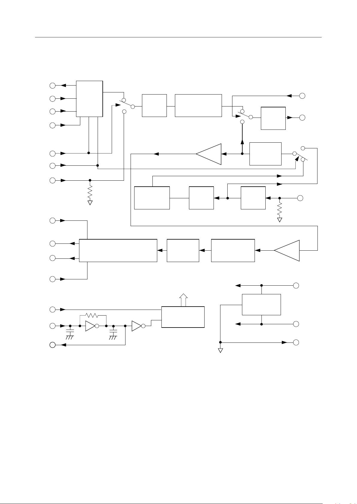
BLOCK DIAGRAM
ST
SD
PRE
SIN
Modu-
lator
1
0
RC
LPF
Transmit
LPF
1
0
RC
LPF
FT
AO
ME
BR
TI
CF
RT
RD
CT
MCS
X1
Timing
Re-generator
Mixer
PDF
*
Clock
Generator
PRE
LPF
LIM
Delay
Detector
Receive
RC
LPF
Signal
Ground
BPF
SH
0
1
AI
V
DD
GND
X2
* Post Detection Filter
SG
2/15
Page 3
¡ Semiconductor MSM6882-3/6882-5
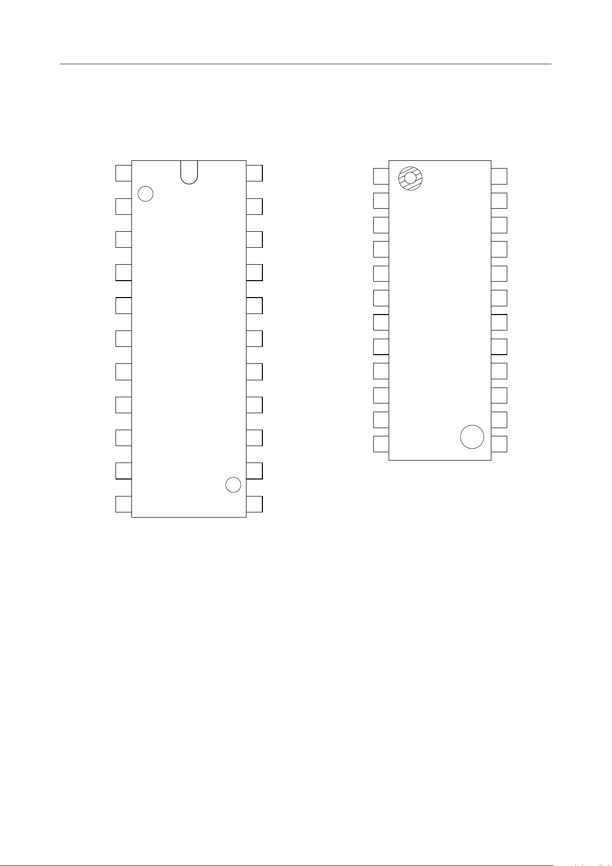
PIN CONFIGURATION (TOP VIEW)
1
X1
2 21X2 FT
3
4
5
6
7
8
9
10
22
V
DD
20MCS CT
19ME CF
18SD RT
17ST RD
16SIN CDO
15PRE CDT
14BR AI
13SG AO
1
X1
2
X2
3
MCS
4
ME
5
SD
6
ST
7
SIN
8
PRE
9
BR
10 15SG AI
11
12
24
V
23
FT
22
CT
21
CF
20
RT
19
(NC)
18
RD
17
CDO
16
CDT
14GND AO
13GND TI
DD
11
GND
22-Pin Plastic DIP
NC : No connect pin
12
TI
24-Pin Plastic SOP
3/15
Page 4
¡ Semiconductor MSM6882-3/6882-5
PIN DESCRIPTION
Name Description
X1
X2
Crystal connection pins.
A 3.6864 MHz or 7.3728 MHz crystal shall be connected.
When an external clock is applied for MSM6882's oscillation source, it has to be input to X2.
In this case, X2 has to be AC-coupled by the capacitor of 200 pF. X1 shall be left open.
Master clock selection.
MCS
ME
SD
ST
MCS
Modulator enable.
When a "high" is input on this pin, MSK modulator output is connected to the input of transmit
LPF.
When a "low" is input on this pin, TI is connected to the input of transmit LPF.
Send data input.
The data on this pin is synchronized with the rising edge of ST and input to MSK modulator
as an actual transmit data.
This timing signal is used to latch serial input data on the SD pin.
The frequency of ST coincides with the transmission bit rate.
Modulation method selection.
Data put on this pin selects either SINE FAST FSK or COSINE FAST FSK.
Crystal or External Clock
0 3.6864 MHz
1 7.3728 MHz
SD
ST
MSK Modulated Data
SIN
PRE
Data (2400 bps)
Sine Fast FSK
Cosine Fast FSK
Preamble or data transmission selection.
When a "low" is input on this pin, the data put on the SD pin is output on the AO pin.
When a "high" is input on this pin, the data put on the SD pin is neglected and preamble data
is output.
Data put on PRE is latched on the rising edge of ST.
Preamble means to modulate as 010101...pattern.
010011
4/15
Page 5
¡ Semiconductor MSM6882-3/6882-5
Name Description
Baud rate selection.
BR
SG
TI
Master Clock
(MHz)
7.3728
3.6864
3.6864
MCS BR
11
10
00
11
10
Bit Rate
(bps)
2400
1200
1200
1200
600
Carrier Freq. (Hz)
Mark Space
1200
1200
1200
600
600
2400
1800
1800
1200
900
Built-in analog signal ground.
The DC voltage is approximately half of V
, so the analog interfaces signals of AI, AO, and TI
DD
with peripheral circuits which must be implemented by AC-coupling. To make this voltage
source impedance lower and ensure the device performance of this device, more than 0.1 mF
bypass capacitors should be connected from SG to GND and from SG to V
DD
.
Ground. (0 V)GND
Voice signal input.
The signal input to this pin can be sent out to AO through the transmit LPF, the characteristics
of which, gives the splatter filter for voice band signal.
When this function is used, digital "0" must be input to ME.
TI is biased to SG through internal resistor.
Transmit analog signal output.
The data put on ME and FT can set the status of AO as follows.
AO
FT
"1" "1"
ME Transmit LPF State of AO
MSK Signal
Power On
"1" "0" Voice Signal
"0" "1" The Output of Receive BPF
Power Down
"0" "0" No-signal (SG level)
TI
Power down
Transmit LPF
+
–
AO
AI
SD
Modu-
lator
SG
Receive BPF
The state when FT and ME = "0" is shown above. When the input digital data on FT changes to
"1" from "0", AO remains to be connected to SG during about 2 ms and after that, and AO is
switched to transmit LPF.
This delay time prevents AO from outputting meaningless signal during transient time from
power down to on of LPF.
5/15
Page 6

¡ Semiconductor MSM6882-3/6882-5
Name Description
AI
Receive analog signal input.
AI is biased internally to SG with about 100 kW same as TI.
CDT
CDO
RD
RT
CF
Device test.
This pin should be connected to GND.
Device test.
This pin should be opened.
Demodulated serial data output.
This data is synchronized with the re-generated timing clock RT.
Receive data timing clock output.
This signal is re-generated by internal digital PLL.
Synchronizing to negative edge of RT, RD is output.
RT
RD
Receive data timing clock is re-generated by digital PLL of which phase correcting speed can
be selected with CF.
When a digital "1" is put on CF and phase difference between receive data timing and RT is
more than 22.5 degree, phase correcting speed is high. In this case, as the phase difference
enters within 22.5 degrees, that speed changes to low immediately.
When digital "0" is input to CF, phase correcting speed of PLL remains low regardless of the
phase difference.
Usually, CF is connected to digital "1".
V
CT
FT
DD
PLL's lock-in characteristics can be selected with CT.
When digital "1" is put on CT, PLL requires max. 50 bit alternative data pattern. On the other
hand, when digital "0" is input to CT,
PLL can be locked in below 18-bit data.
CF
CT
1
0
MIN
—
TYP
—
MAX
18
UNIT
bit
1
1
—
—
50
Control signal for the internal connection of AO.
Refer to column AO.
When digital "0" is input to this pin, transmit LPF enters in power down mode, but the output
buffer operational amplifier remains active. In this case, AO is at SG level.
Power supply.
MSM6882-3: 3.6 V
MSM6882-5: 5 V
This device is sensitive to supply noise as switched capacitor techniques are utilized.
A bypass capacitor of more than 2.2 mF between V
and GND is indispensable to ensure the
DD
performance.
6/15
Page 7

¡ Semiconductor MSM6882-3/6882-5
ABSOLUTE MAXIMUM RATINGS
Parameter Symbol Condition Rating Unit
Power Supply Voltage V
Input Voltage *1 V
Operating Temperature T
Storage Temperature T
DD
op
STG
Ta = 25°C
I
With respect to GND
—
—
–0.3 to 7.0
–0.3 to VDD + 0.3
–25 to 70
–55 to 150
V
°C
*1 MCS, ME, SD, SIN, PRE, BR, TI, AI, CDT, CF, CT, FT
RECOMMENDED OPERATING CONDITIONS
Parameter Symbol Condition Typ. Unit
V
Power Supply Voltage V
DD
With respect to GND
Min. Max.
*1
*2
3.63.0 4.0
54.5 5.5
GND — 0——
Operating Temperature
T
op
—25–25 70 °C
MCS = "1" 7.37287.3721 7.3735
Crystal Resonant Frequency
Data Speed T
C1 — 2.2——
C2 — 0.1——
C3 — 0.047——
C4 R
C5 — 0.047——
f
X' TAL
—
—
—
—
—
MCS = "0" 3.68643.6860 3.6868
MHz
S
BR = "0" 1200——
≥ 40 kW 0.047——
LX
MCS = "1", BR = "1" 2400——
bit/sec
mF
C6 — 0.1———
Oscillation Frequency
Temperature
Characteristics
Crystal
Equivalent Series
Resistance
—
—
—
—
At –30°C to +70°C —–100 +100
— 7.3728——
MHz
25 ±5°C —–100 +100Frequency Deviation
ppm
—
——50W
Oscillation Frequency
Temperature
Characteristics
Crystal
Equivalent Series
Resistance
*1 MSM6882-3
*2 MSM6882-5
—
—
—
—
—
—
—
16——pFLoad Capacitance
— 3.6864——
25 ±5°C —–100 +100Frequency Deviation
At –30°C to +70°C —–100 +100
—
—
—— 100 W
16——pFLoad Capacitance
MHz
ppm
7/15
Page 8

¡ Semiconductor MSM6882-3/6882-5
ELECTRICAL CHARACTERISTICS
DC Characteristics
(MSM6882-3: V
(MSM6882-5: V
DD
= 5 V ±0.5 V, Ta = –25˚C to 70˚C)
DD
Parameter Symbol Condition Typ. UnitMin. Max.
Normal Operating Mode
I
Power Supply Current
DD
*1
FT = "1"
Power Down Mode
I
Input Leakage Current *2
DDS
I
IL
I
IH
V
IL
FT = "0"
VIN = 0 V —–10 10
VIN = V
DD
*1
Input Voltage *2
1.8
Output Voltage *1 *3
V
V
V
OL1
OH1
IH
IOL = 10 mA/1.6 mA —0
IOH = 10 mA/400 mA—0.8V
*1
2.2
DD
*1 Upper is specified for the MSM6882-3, lower for the MSM6882-5
*2 MCS, ME, SD, SIN, PRE, BR, CF, CT, FT
*3 ST, RD, RT
= 3 V to 4 V, Ta = –25˚C to 70˚C)
4—8
5.5—11
mA
3.5—7
5.0—10
mA
—–10 10
0.6
—0
0.8
—
V
DD
V
0.3
0.4
V
DD
Digital Interface Characteristics
Parameter Symbol Condition Typ. UnitMin. Max.
t
S
Input Data Hold Time t
Output Data Delay Time t
H
D
See Fig.1
—300 —Input Data Set-up Time ns
—300 — ns
See Fig.2 —–300 300 ns
8/15
Page 9

¡ Semiconductor MSM6882-3/6882-5
Analog Interface Characteristics
Transmit signal output (AO)
Parameter Symbol Condition Typ. UnitMin. Max.
f
V
f
f
f
V
M1
S1
M2
S2
OX
OPP
OX
LX
LX
OSX
1200
bps
Carrier Frequency
2400
bps
Carrier Level *1
Output Amplitude
*1
Output Resistance
Output Load Resistance
Output Load Capacitance
Output DC Voltage
Voice signal input (TI)
Parameter Symbol Condition Typ. UnitMin. Max.
GT VAO/V
Input Signal Level
Input Resistance
*1
V
TI
R
TI
= 3 V to 4 V, Ta = –25˚C to 70˚C)
DD
= 5 V ±0.5 V, Ta = –25˚C to 70˚C)
DD
12001199 1201
18001799 1801SD = "0"
12001199 1201SD = "1"
FT = "1"
ME = "1"
BR = "0"
BR = "1"
(MSM6882-3: V
(MSM6882-5: V
SD = "1"
24002399 2401SD = "0"
≥ 40 kW
R
L
C
£ 40 pF
L
FT = "1"
ME = "1"
FT = "1"
ME = "0"
–3–7 –1
0–3 2
2.01.4 —
3.02.2 —
50——W—R
—40 — kW—R
——40pF—C
0.48V
TI
—
f
£ 4 kHz 10040 300 kW
TI
FT = "1"
ME = "0"
DD
0.50V
0–2 +2Voltage Gain dB
——
DD
0.52V
Hz
dBm
*2
V
p-p
V—V
DD
–4 dBm
0
*2
Built-in signal ground (SG)
Parameter Symbol Condition Typ. UnitMin. Max.
DC Voltage V
SG
Without DC Load V
0.48V
DD
Receive signal input (AI)
Parameter Symbol Condition Typ. UnitMin. Max.
Input Resistance R
V
Receive Signal Level
V
1200 bps
Bit Error Rate
BER
2400 bps
AI
IR1
IR2
S/N at AI
SIN = "1"
f
£ 4 kHz 100 kW40 300
AI
BR = "0"
—
S/N
BR = "1"
7 dB
11 dB
10 dB 2 ¥ 10
14 dB 2 ¥ 10
——
——
——
——
*1 Upper is specified for the MSM6882-3, lower for the MSM6882-5
*2 0 dBm = 0.775 Vrms
0.50V
DD
— dBm–30 0
—*2–24 0
–3
2 ¥ 10
–5
2 ¥ 10
–3
–5
0.52V
DD
9/15
Page 10

¡ Semiconductor MSM6882-3/6882-5
Re-generated receive data timing clock output (RT)
Parameter Symbol Condition Typ. UnitMin. Max.
Data Bit Number for PLL'
Lock-in
N
N
PLL1
PLL2
CF = "1"
CT= "0"
CT= "1"
*3
——18
——50
bit
*3 Data bit number to lock-in within 22.5 degree
10/15
Page 11

¡ Semiconductor MSM6882-3/6882-5
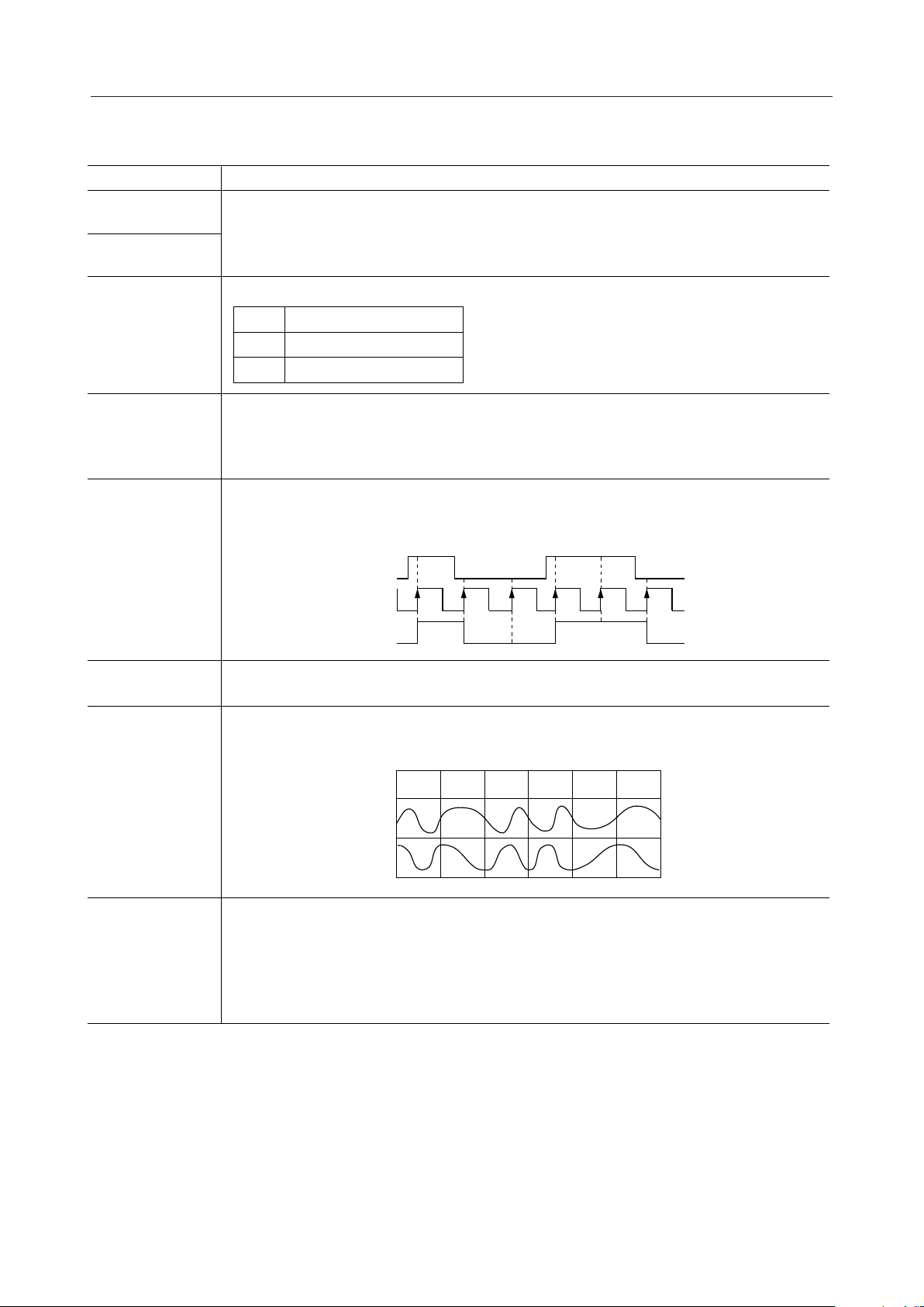
TIMING DIAGRAM
ST
SD, PRE
RT
50%
50%
t
S
t
H
Figure 1 Input Data Timing
50%
RD
50%
t
D
Figure 2 Output Data Timing
11/15
Page 12

¡ Semiconductor MSM6882-3/6882-5
BUILT-IN FILTER FREQUENCY CHARACTERISTICS
GAIN (dB)
0
–10
–20
–30
–40
–50
–60
–70
1
Transmit Low-Pass Filter
2345678910
FREQ (kHz)
GAIN (dB)
0
–10
–20
–30
–40
–50
–60
–70
0.5
Receive Band-Pass Filter
1 1.5 2 2.5 3 3.5 4
FREQ (kHz)
Note: When BR = "1", frequency converter circuit (MIXER) is prepared before the receive BPF.
Therefore, 1200 Hz input signal is converted to 3600 Hz at BPF output for example.
12/15
Page 13

¡ Semiconductor MSM6882-3/6882-5
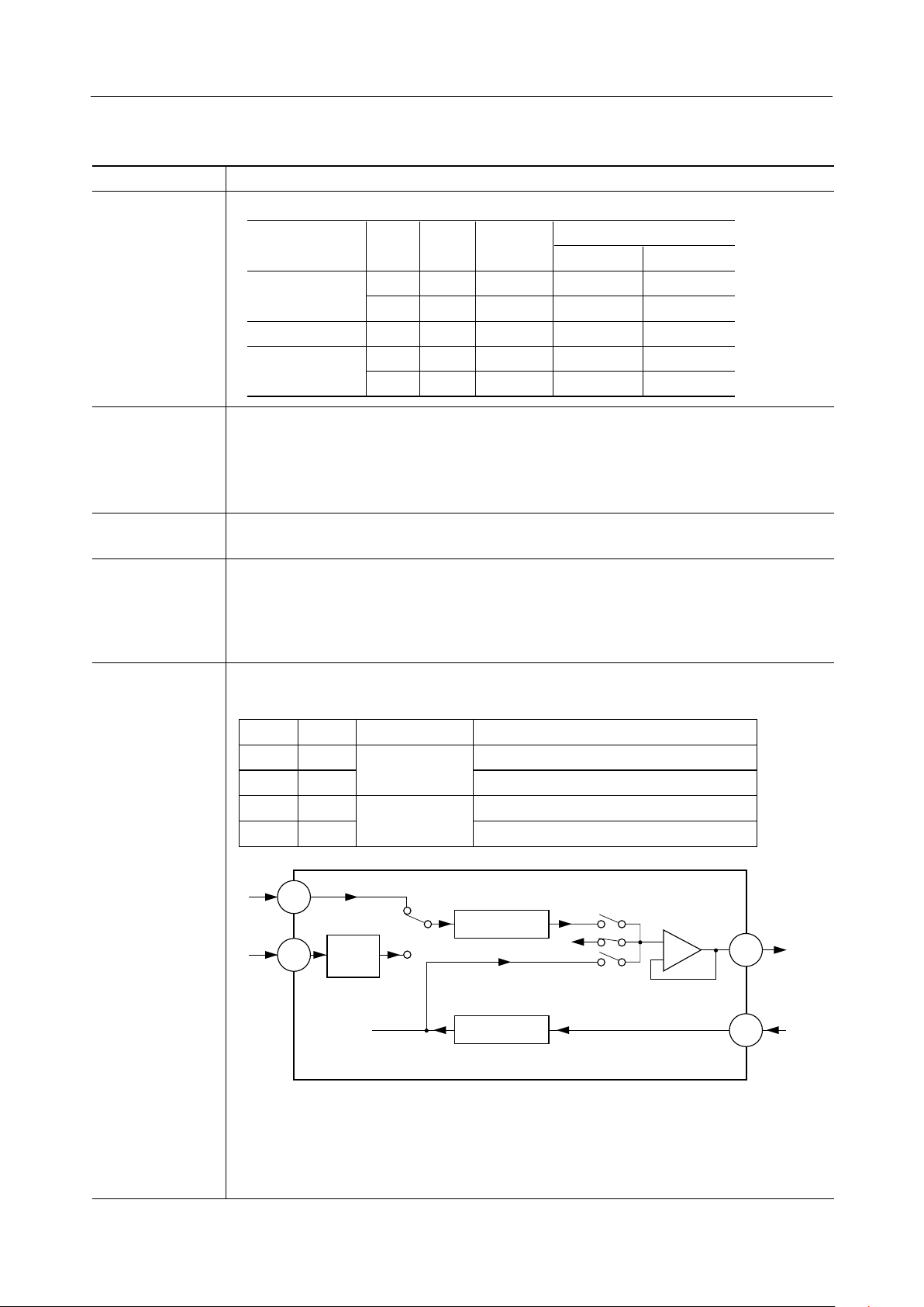
APPLICATION CIRCUIT
V
DD
Crystal
7.3728 MHz
C6 C2
V
DD
X1
1
X2
2
MCS
3
ME
4
SD
5
ST
6
SIN
7
PRE
8
BR
9
SG AO
10
GND TI
11
V
DD
FT
CT
CF
RT
RD
CDO
CDT
AI
22
21
20
19
18
17
16
15
14
13
12
C1
C3
C4
C5
13/15
Page 14

¡ Semiconductor MSM6882-3/6882-5
PACKAGE DIMENSIONS
(Unit : mm)
DIP22-P-400-2.54
Package material
Lead frame material
Pin treatment
Solder plate thickness
Package weight (g)
Epoxy resin
42 alloy
Solder plating
5 mm or more
1.90 TYP.
14/15
Page 15

¡ Semiconductor MSM6882-3/6882-5
(Unit : mm)
SOP24-P-430-1.27-K
Mirror finish
Package material
Lead frame material
Pin treatment
Solder plate thickness
Package weight (g)
Epoxy resin
42 alloy
Solder plating
5 mm or more
0.58 TYP.
Notes for Mounting the Surface Mount Type Package
The SOP, QFP, TSOP, SOJ, QFJ (PLCC), SHP and BGA are surface mount type packages, which
are very susceptible to heat in reflow mounting and humidity absorbed in storage.
Therefore, before you perform reflow mounting, contact Oki’s responsible sales person for the
product name, package name, pin number, package code and desired mounting conditions
(reflow method, temperature and times).
15/15
 Loading...