

Page 1

E2B0046-27-Y2
¡ Semiconductor MSM6794
¡ Semiconductor
This version: Nov. 1997
Previous version: Mar. 1996
MSM6794
DOT MATRIX LCD DRIVER WITH 128-CHANNEL RAM
GENERAL DESCRIPTION
The MSM6794 is a dot matrix graphic liquid crystal display LSI device to display bit maps.
It drives an LCD panel for dot matrix graphic display under the control of a 4- or 8-bit
microcomputer.
All necessary functions for driving a bit map type LCD are built in on one chip. Therefore,by
using the MSM6794, a bit map type dot matrix graphic liquid crystal display system can be
implemented with a small number of chips.
Since 1-bit data of the display RAM corresponds to the light-on/off of 1-dot of the LCD panel (bit
map system), a flexible display, including kanji display, is possible. One chip comprises a graphic
display system of a maximum of 128¥48 dots. This display can be expanded by using multiple
chips.
The MSM6794 uses CMOS process. Since it is an internal RAM type, the MSM 6794 features low
power consumption, and is suited to display for battery-driven portable equipment.
FEATURES
• Segment outputs : Maximum of 128
• Common outputs : Maximum of 48
• Display duty : 1/33, 1/41, 1/44, 1/48
• Bit map type internal RAM : 6,144 bits (128¥48 bits)
• Display data I/F : 8-bit parallel/serial switchable
• Standby function by program
• LCD drive bias resistor (externally connected)
• Built-in voltage multiplier circuit
• LOGIC voltage : 2.7 to 5.5V
• LCD driving voltage : VBI 5 to 12V (positive voltage)
• Low current consumption : Maximum of 10mA (in standby mode)
• Number of pads : 224
1/34
Page 2
¡ Semiconductor MSM6794
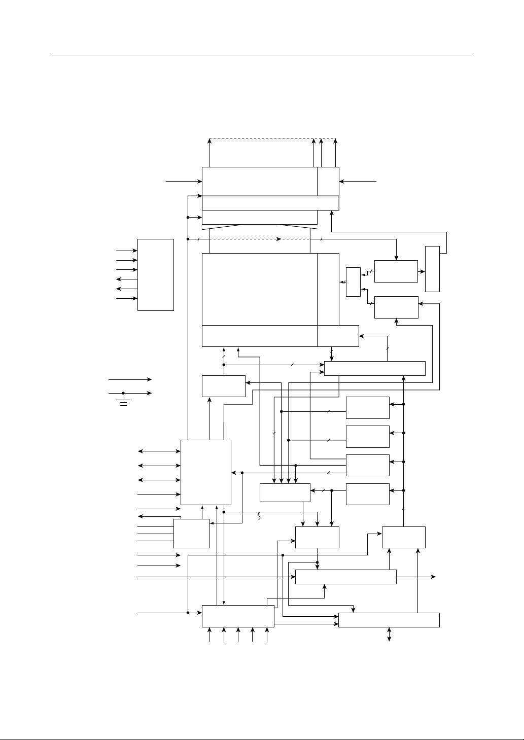
BLOCK DIAGRAM
COM48
SEG1
SEG128 COM1
LCD drive power supply
V1, V3, V4, V6
V
VC1
VC2
VS1
VS2
DT
to V
V
DD1
DD4
V
to V
SS1
SS3
IN
DF
LCDCK
FLM
M/S
RESET
CO
OSC1
OSC2
OSC3
TEST1
TEST2
multiplier
SI
Voltage
circuit
Segment driver
Level shifter
Data latch
2 2
RAM
128 × 48 bit
display memory
X decoder
5
X address
counter
8
Timing
generator
MPX
Clock
frequency
divider
circuit
BUSY
driver
Common
6
6
MPX
Y decoder
Memory
/output
2
8
input
buffer
6
8-, 6-bit conversion circuit
X address
5
register
Y address
6
register
Control
register
7
7
Address
register
MPX MPX
8-bit Serial register
LCD drive power supply
V1, V2, V5, V6
Common
counter
Decoder
Y address
counter
8
8
SO
P/S
I/O control
SHT CS WR RD RS
Input/output buffer
DB7 to DB0
2/34
Page 3
¡ Semiconductor MSM6794
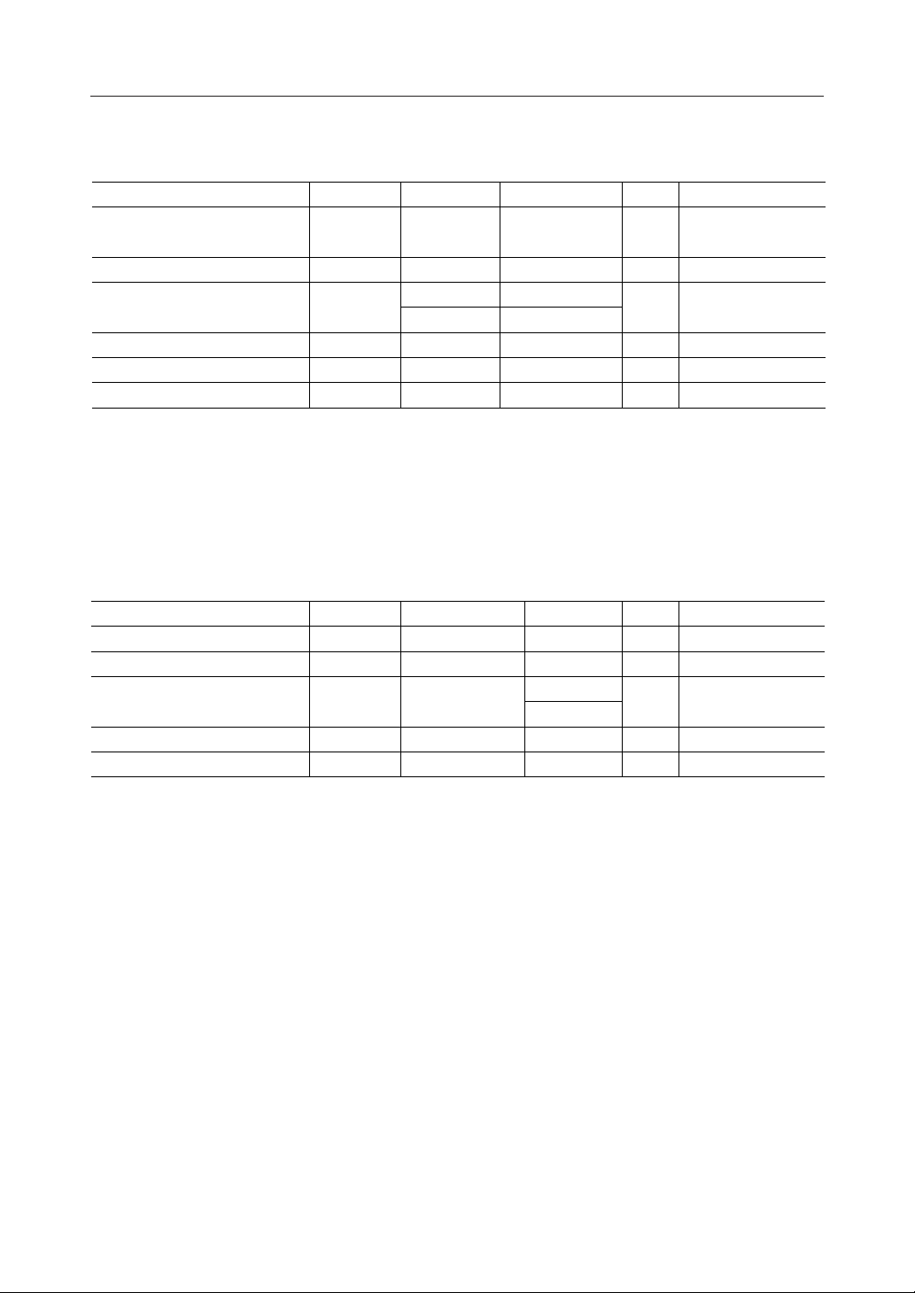
ABSOLUTE MAXIMUM RATINGS
Parameter Symbol Condition Rating Unit Applicable Pins
Supply voltage
Bias voltage
Voltage multiplication
reference voltage
Input voltage
Power dissipation
Storage temperature
*2
*3
–0.3 to +7
–0.3 to +14
–0.3 to +7
–0.3 to +4.6
–0.3 to V
*1
–55 to +150
DD
+0.3
V
DD
V
BI
V
IN
V
I
P
D
T
STG
Ta=25˚C,
V
DD1-4–VSS1-3
Ta=25˚C,V1–V6
V
IN–VSS1-3
VIN–V
SS1-3
Ta=25˚C
—
—
V
V
V
V
mW
˚C
V
DD1-4
V1, V6
V
IN, VSS1-3
All Inputs
—
—
, V
SS1-3
Ta : ambient temperature
*1 Power dissipation depends on the heat radiation in a device attach condition. Set junction
temperature to 150˚C or lower.
*2 Ta = 25˚C; when doubler is used.
*3 Ta = 25˚C; when tripler is used.
RECOMMENDED OPERATING CONDITIONS
Parameter Symbol Condition Range Unit Applicable Pins
Supply voltage
Bias voltage
Voltage multiplicatipon
reference voltage
Operating frequency
Operating temperature
1
2.7 to 5.5
5 to 12
1 to V
DD
1 to 4
270 to 500
–25 to +85
V
V
V
kHz
˚C
V
DD
V
BI
V
IN
f
op
T
op
V
DD1-4–VSS1-3
V1–V6
VIN–V
SS1-3
See Note 1 on p.6
2
—
V
DD1-4, VSS1-3
V1, V6
V
, V
IN
SS1-3
OSC1
—
1 For bias potential, V1 has the highest potential and V6 has the lowest potential. Use V6 at the
same potential as V
SS1
to V
SS3
.
2 RC oscillation and external input clock frequency (when frequency dividing ratio is 1).
For divided frequency operation, clock frequency after dividing must be within this range.
3/34
Page 4
¡ Semiconductor MSM6794
ELECTRICAL CHARACTERISTICS
DC Characteristics (1)
(V
=2.7 to 4.5V, VBI=5 to 12V, Ta=–25 to +85˚C)
DD
Parameter Symbol Condition Min. Typ. Max. Unit. Applicable Pin
"H" input voltage 1
"H" input voltage 2
"H" input voltage 3
"L" input voltage 1
"L" input voltage 2
"L" input voltage 3
DD
DD
DD
—
—
—
—
—
—
V
V
DD
V
0.2V
0.2V
0.2V
DD
DD
V
IH1
V
IH2
V
IH3
V
IL1
V
IL2
V
IL3
—
—
—
—
—
—
0.8V
0.8V
0.8V
0
0
0
DD
DD
DD
V
V
V
V
V
Unit.
DB0-7, LCDCK, FLM, DF
Other input pins
DB0-7, LCDCK, FLM, DF
Other input pins
Input pins excluding
"H" input current 1
I
IH1
V
I=VDD
—
—
5
µA
DB0-7
FLM and DF
"H" input current 2
I
IH2
VI=V
DD
–5
—
5
DB0-7, LCDCK, FLM, DF
µA
Input pins excluding
"L" input current I
I
IL1
VI=0V
–5
—
—
µA
DB0-7
FLM and DF
"L" input current 2
OFF leakage
current
"H" output voltage 1
"H" output voltage 2
"L" output voltage 1
"L" output voltage 2
Multiplied voltage 1
Doubler output
Multiplied voltage 2
Tripler output
COM output
resistance
SEG output
resistance
I
IL2
I
off
V
OH1
V
OH2
V
OL1
V
OL2
V
DB
V
TR
R
C
R
S
V
V
I=VDD
I
=–1.0mA
O
=–1.0mA
I
O
=1.0mA
I
O
=1.0mA
I
O
=–500µA
I
O
=350kHz
f
osc
=–500µA
I
O
=350kHz
f
osc
I
=±50µA
O
=±20µA
I
O
=0V
I
or 0V
–5
–5
0.9V
0.9V
—
—
V
IN
–0.5
V
IN
–1.0
—
—
×2
×3
DD
DD
—
—
—
—
—
—
—
—
—
—
—
—
0.1V
0.1V
—
—
10
20
5
5
DD
DD
DB0-7, LCDCK, FLM, DF
µA
µA
CO, LCDCK, FLM, DF, SO
V
V
V
V
DB0 to DB7
CO, LCDCK, FLM, DF, SO
DB0 to DB7
V
V
kΩ
kΩ
COM1 to COM48
SEG1 to SEG128
During display
Supply Current 1
I
DD1
External clock
= 350kHz
f
osc
—
—
450
µA
During display
Supply Current 2
I
DD2
Internal
oscillation
= 350kHz
f
osc
—
360
700
µA
OSC1
OSC1
, LCDCK,
, LCDCK,
SO
VS2
VS2
V
DD
V
DD
Supply Current 3
Oscillation
frequency
I
f
DDS
OSC
During standby
R
=18kΩ
f
=56pF
C
f
See Note 3 on p.6
—
292
—
350
10
437
µA
kHz
V
DD
OSC1, OSC2, OSC3
4/34
Page 5
¡ Semiconductor MSM6794
DC Characteristics (2)
=4.5 to 5.5V, VBI=5 to 12V, Ta=–25 to +85˚C)
(V
DD
Parameter Symbol Condition Min. Typ. Max. Unit Applicable Pin
"H" input voltage 1
"H" input voltage 2
"H" input voltage 3
"L" input voltage 1
"L" input voltage 2
"L" input voltage 3
"H" input current 1
"H" input current 2
"L" input current I
"L" input current 2
OFF leakage
current
"H" output voltage 1
"H" output voltage 2
"L" output voltage 1
"L" output voltage 2
Multiplied voltage 1
Doubler output
Multiplied voltage 2
Tripler output
V
IH1
V
IH2
V
IH3
V
IL1
V
IL2
V
IL3
I
IH1
I
IH2
I
IL1
I
IL2
I
off
V
OH1
V
OH2
V
OL1
V
OL2
V
DB
V
TR
— 0.8V
— 0.8V
— 0.8V
— 0 — 0.2V
— 0 — 0.2V
— 0 — 0.2V
—VDDV OSC1
DD
—VDDV
DD
—VDDV Other input pins
DD
DD
DD
DD
DB0-7, LCDCK, FLM, DF
V OSC1
V
DB0-7, LCDCK, FLM, DF
V Other input pins
Input pins excluding
VI=V
DD
—— 5µA
DB0-7
FLM and DF
VI=V
DD
–5 — 5 µA
DB0-7, LCDCK, FLM, DF
Input pins excluding
V
=0V –5 — — µA
I
DB0-7
FLM and DF
V
=0V –5 — 5 µA
I
VI=V
/0V –5 — 5 µASO
DD
IO=–1.5mA 0.9V
IO=–1.5mA 0.9V
IO=1.5mA — — 0.1V
IO=1.5mA — — 0.1V
I
=–500µA
O
f
=350kHz
osc
I
=–500µA
O
f
=350kHz
osc
V
–0.5
V
–1.0
IN
IN
— — V CO, LCDCK, FLM, DF, SO
DD
— — V DB0 to DB7
DD
DD
DD
×2
— — V VS2
×3
— — V VS2
DB0-7, LCDCK, FLM, DF
V CO, LCDCK, FLM, DF, SO
V DB0 to DB7
, LCDCK,
, LCDCK,
COM output
resistance
SEG output
resistance
Supply Current 1
Supply Current 2
Supply Current 3
Oscillation
frequency
I
I
I
f
R
C
R
S
DD1
DD2
DDS
OSC
See Note 3 on p.6
I
=±50µA——10kΩCOM1 to COM48
O
I
=±20µA——20kΩSEG1 to SEG128
O
During display
External clock
f
= 350kHz
osc
— — 450 µA V
During display
Internal
oscillation
f
=350kHz
osc
During standby
R
=22kΩ
f
C
=56pF
f
— 360 700 µA V
——10µA V
292 350 437 kHz OSC1, OSC2, OSC3
DD
DD
DD
5/34
Page 6
¡ Semiconductor MSM6794
g
g
Notes: 1. Voltage multiplication reference voltage is = VDD maximum when the multiplied
voltage is 12V or less.
The voltage multiplication reference voltage is 4V maximum when the multiplied
voltage is 12V or more (tripler output).
Condition: f
= 350kHz
osc
Voltage multiplier circuit configuration: connect as in the following diagram.
<Usin
V
IN
VC1
VC2
VS1
VS2
tripler>
Voltage multiplication
reference voltage
Doubler output
4.7µF
4.7µF
+
+
<Usin
Voltage multiplication
reference voltage
Tripler output
4.7µF
4.7µF
4.7µF
+
+
+
2. If the multiplied voltage output and bias power supply are directly connected, the
voltage multiplier circuit operation may malfunction due to bias power supply noise.
A countermeasure for noise is necessary, such as inserting a series resistor to prevent
noise from entering multiplied voltage output (VS1, VS2).
+
4.7µF
VS1
V
IN
VC1
VC2
VS1
VS2
doubler>
100Ω
Tripler output
+
VS2
4.7µF
3. RC oscillation circuit configuration: connect as in the following diagram.
R
= 18kΩ ± 2 % (V
OSC1
C
f
R
f
OSC2
f
= 22kΩ ± 2 % (V
R
f
C
= 56pF ± 5 %
f
OSC3
= 2.7 to 4.5V)
DD
= 4.5 to 5.5V)
DD
6/34
Page 7
¡ Semiconductor MSM6794
AC Characteristics
Parallel interface (1)
Parameter Symbol Condition Min Max Unit
RD "H" level width
RD "L" level width
WR "H" level width
WR "L" level width
WR-RD "H" level width
CS, RS setup time
CS, RS hold time
Write data setup time
Write data hold time
Read data output delay time
Read data hold time
External clock "H" level width
External clock "L" level width
RESET pulse width
External clock rise time, fall time
Parallel interface (2)
Parameter Symbol Condition Min Max Unit
RD "H" level width
RD "L" level width
WR "H" level width
WR "L" level width
WR-RD "H" level width
CS, RS setup time
CS, RS hold time
Write data setup time
Write data hold time
Read data output delay time
Read data hold time
External clock "H" level width
External clock "L" level width
RESET pulse width
External clock rise time, fall time tr, t
t
WRH
t
WRL
t
WWH
t
WWL
t
WWRH
t
AS
t
AH
t
DSW
t
DHW
t
DDR
t
DHR
t
WCH
t
WCL
t
WRE
t
, t
r
f
t
WRH
t
WRL
t
WWH
t
WWL
t
WWRH
t
AS
t
AH
t
DSW
t
DHW
t
DDR
t
DHR
t
WCH
t
WCL
t
WRE
f
(V
=2.7 to 4.5V, VBI=5 to 12V, Ta=–25 to +85˚C)
DD
— 200 — ns
— 200 — ns
— 200 — ns
— 200 — ns
— 200 — ns
—50—ns
—10—ns
—50—ns
—20—ns
CL=50pF — 170 ns
—20—ns
— 200 — ns
— 200 — ns
— 2.0 — µs
— — 100 ns
(V
=4.5 to 5.5V, VBI=5 to 12V, Ta=–25 to +85˚C)
DD
— 150 — ns
— 150 — ns
— 150 — ns
— 150 — ns
— 150 — ns
—50—ns
—10—ns
—50—ns
—20—ns
CL=50pF — 130 ns
—20—ns
— 150 — ns
— 150 — ns
— 2.0 — µs
— — 20 ns
7/34
Page 8
¡ Semiconductor MSM6794
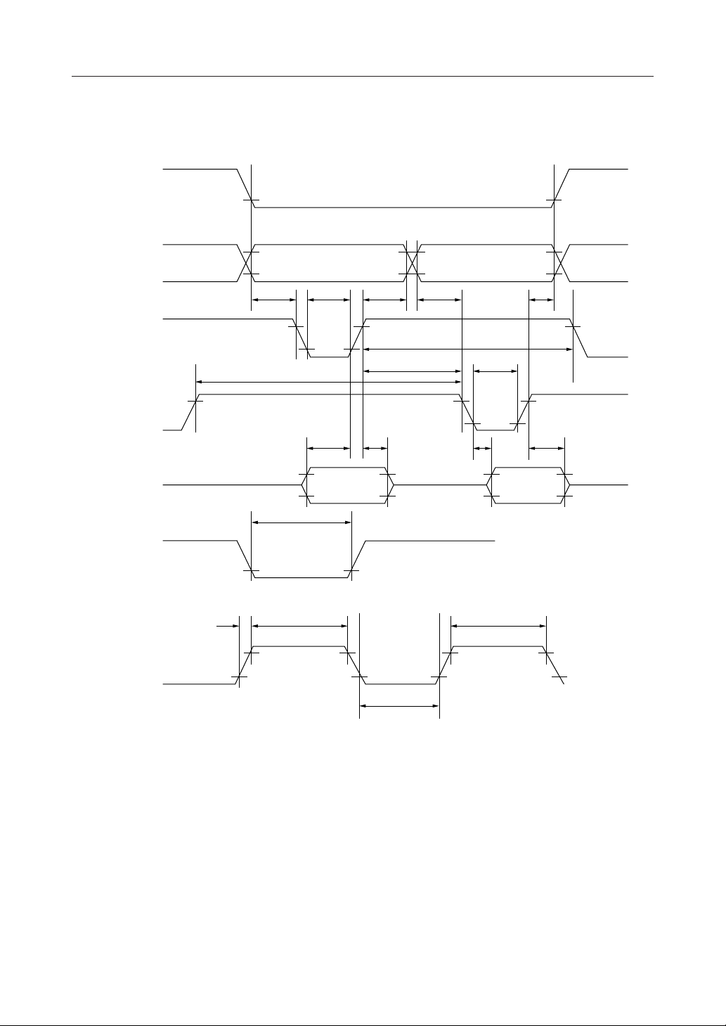
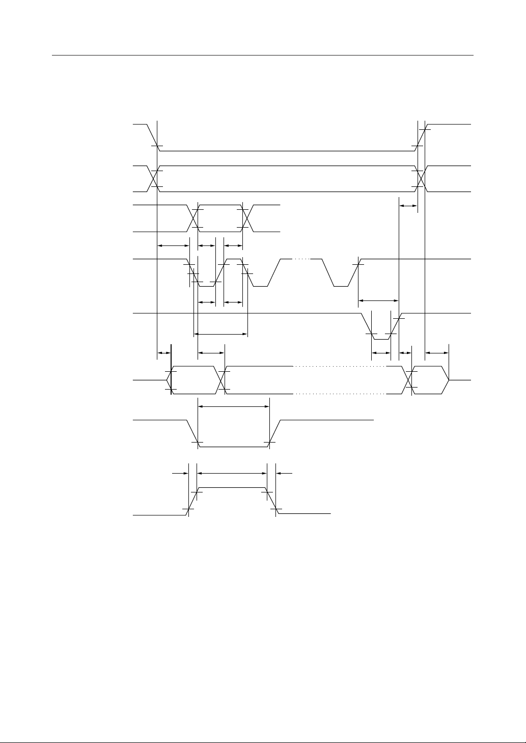
Parallel Interface Timing Diagram
—
V
IH
CS
RS
WR
RD
—
V
IL
—
V
IH
—
V
IL
t
AS
—
V
IH
—
V
IL
—
V
IH
—
V
IL
t
WRH
t
t
WWL
DSW
t
DHW
t
AH
t
WWH
t
WWRH
t
AS
t
WRL
t
DDR
t
AH
t
DHR
DB0-DB7
RESET
OSC1
V
IH
V
IL
t
WRE
—
V
IL
t
r
—
V
IH
—
V
IL
t
f
t
WCL
V
OH
V
OL
t
WCH
V
IH
V
OH
, V
0.8V
=
0.9V
=
= 0.2V
DD
IL
DD
, V
= 0.1V
DD
OL
DD
8/34
Page 9
¡ Semiconductor MSM6794
Serial interface (1)
=2.7 to 4.5V, VBI=5 to 12V, Ta=–25 to +85˚C)
(V
DD
Parameter Symbol Condition Min Max Unit
CS, RS setup time
CS, RS hold time
S1 setup time
S1 hold time
SHT "H" pulse width
SHT "L" pulse width
SHT clock cycle time
SO ON delay time
SO output delay time
SO OFF delay time
BUSY delay time
WR setup time
WR "L" pulse width
RESET pulse width
t
SAS
t
SAH
t
IS
t
IH
t
WSHH
t
WSHL
t
SYS
t
ON
t
DS
t
OFF
t
BUSY
t
SHS
t
WWL
t
WRE
—60—ns
—15—ns
— 100 — ns
—15—ns
— 100 — ns
— 100 — ns
— 400 — ns
CL=50pF — 200 ns
CL=50pF 0 200 ns
— — 50 ns
CL=50pF — 200 ns
— 100 — ns
— 120 — ns
— 2.0 — µs
External clock rise time, fall time tr, t
Serial interface (2)
Parameter Symbol Condition Min Max Unit
CS, RS setup time
CS, RS hold time
S1 setup time
S1 hold time
SHT "H" pulse width
SHT "L" pulse width
SHT clock cycle time
SO ON delay time
SO output delay time
SO OFF delay time
BUSY delay time
WR setup time
WR "L" pulse width
RESET pulse width
f
t
SAS
t
SAH
t
IS
t
IH
t
WSHH
t
WSHL
t
SYS
t
ON
t
DS
t
OFF
t
BUSY
t
SHS
t
WWL
t
WRE
— — 100 ns
=4.5 to 5.5V, VBI=5 to 12V, Ta=–25 to +85˚C)
(V
DD
—50—ns
—10—ns
—50—ns
—10—ns
—80—ns
—80—ns
— 200 — ns
CL=50pF — 100 ns
CL=50pF 0 100 ns
— — 20 ns
CL=50pF — 100 ns
—50—ns
—80—ns
— 2.0 — µs
External clock rise time, fall time tr, t
f
— — 20 ns
9/34
Page 10
¡ Semiconductor MSM6794
Serial Interface Timing Diagram
—
V
CS
RS
SI
SHT
WR
IH
—
V
IL
—
V
IH
—
V
IL
—
V
IH
—
V
IL
t
SAS
—
V
IH
—
V
IL
—
V
IH
—
V
IL
50%
t
ON
t
WSHL
t
t
IS
IH
t
WSHH
t
SYS
t
DS
t
SAH
t
SHS
t
WWLtBUSYtOFF
SO
RESET
OSC1
—
V
V
V
V
V
“Z”
OH
—
OL
t
WRE
—
IL
t
r
—
IH
—
IL
t
f
= 0.8VDD, VIL = 0.2V
V
IH
VOH = 0.9VDD, VOL = 0.1V
DD
DD
“Z”
10/34
Page 11
¡ Semiconductor MSM6794
Serial Interface Input/Output Timing
Input timing
CS
RS
SHT
SI
WR
Output timing
RS
SO
CS
SHT
WR
D7 D6 D5 D4
BUSY BUSY
D7 D6 D5 D4
D3
D2 D1 D0
D3
D2 D1 D0
For SO output, 8 bits after input of the WR pulse are valid.
11/34
Page 12

¡ Semiconductor MSM6794
FUNCTIONAL DESCRIPTION
Pin Functional Description
•CS (Chip Select)
Chip select input pin. "L" is for Select, "H" is for Unselect. Internal registers can be accessed
only when this pin is at "L".
When this pin is "H", the SO pin becomes high impedance.
•WR (Write Enable)
This is a write signal input pin when a parallel interface is used. Data is written to a register
at the rising edge of a signal pulse.
This becomes a latch signal input pin when a serial interface is used.
This pin is normally "H".
•RD (Read Enable)
This is a read signal input pin when a parallel interface is used. Data can be read while the pulse
is "L". This pin is normally "H".
Set this pin to "H" or "L" when a serial interface is used.
•RS (Register Select)
Input pin to select register. Setting this pin to "L" selects the address register. Setting to "H"
selects a register set by the address register.
If this pin is changed from "H" to "L" while a serial interface is used, the SERW bit (D4 bit) of
the address register is automatically reset to "0".
•DB0 to DB7 (Data Buses 0 to 7)
Data input/output pins for parallel interface. These pins are normally in high impedance
status. When RD = "L", each register data is output.
Leave this pin open when a serial interface is used.
•SI (Serial Data Input)
Data input pin for serial interface. Each register data and display data are read at the rising edge
of SHT, and written to the register at the falling edge of WR. 8-bit data just before the rise of
WR is valid data.
Set this pin to "H" or "L" when a parallel interface is used.
•SO (Serial Data Output)
Data output pin for serial interface. Each register data is output synchronizing with the rise of
SHT. For busy/non-busy data, busy ("H") is output after the rise of WR, and automatically
becomes non-busy ("L") after a specified time.
This pin is always in high impedance status when a parallel interface is used.
•SHT (Shift Clock)
Clock input pin for serial interface data input/output. Data is input synchronizing with the
rise of the clock, and data is output synchronizing with the fall of the clock.
This pin is normally in "H".
Set this pin to "H" or "L" when a parallel interface is used.
•P/S (Parallel/Serial Select)
Input pin for selecting parallel interface or serial interface. Setting this pin to "L" selects parallel
interface. Setting to "H" selects serial interface. Do not change the setting value after power
is turned on.
12/34
Page 13

¡ Semiconductor MSM6794
•LCDCK (LCD Clock)
Input/output pin for display data latch clock. This pin is an output pin if master is specified
and is an input pin if slave is specified. To use two or more MSM6794 devices, connect LCDCK
of the master with LCDCK of the slave.
•FLM (First Line Marker)
Input/output pin for the first line marker. This pin is an output pin if master is specified, and
is an input pin if slave is specified. To use two or more MSM6794 devices, connect FLM of the
master with FLM of the slave.
•DF (Display Frequency)
Input/output pin for LCD alternating frame signals. This pin is an output pin if master is
specified, and an input pin if slave is specified. To use two or more MSM6794 devices, connect
DF of the master with DF of the slave.
•OSC1 (Oscillation 1)
Input pin for RC oscillation. Connecting the specified capacitor and resistor to this pin and the
OSC2 and OSC3 pins creates an RC oscillation circuit. To generate an original oscillation clock
externally, input the original oscillation clock to this pin.
•OSC2, OSC3 (Oscillation 2, Oscillation 3)
Output pins for RC oscillation. Connecting the specified capacitor and resistor to these pins
and the OSC1 pin creates an RC oscillation circuit. To generate an original oscillation clock
externally, leave these pins open.
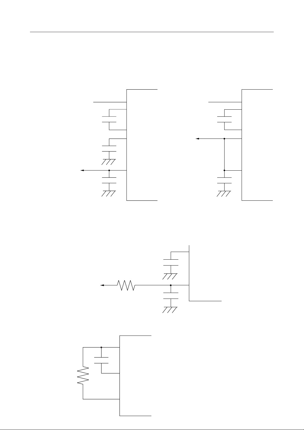
OSC1
OSC2
OSC3
For RC oscillation circuit For external clock input
Oscillation circuit diagram
OSC1
OSC2
OSC3
External clock
Open
Open
M/S (Master/Slave)
Input pin for switching between master and slave. Setting this pin to "L" sets this IC to the IC
at the master side. Setting this pin to "H" sets this IC to the IC at the slave side. Do not change
the setting value after power is turned on.
CO (Clock Output)
Output pin for original oscillation clock. The clock in the same phase as OSC1 is output. To
use two or more MSM6794 devices, connect CO of the master with OSC1 of the slave.
13/34
Page 14

¡ Semiconductor MSM6794
RESET (Reset)
Pin for reset signal input. Setting this pin to "L" sets initial status. For the status of each register
and display after reset input, see "Status of Pins and Registers after Reset Input".
TEST1, TEST2 (Test Signal 1, Test Signal 2)
Test signal input pins. These pins are used by Oki to test. Set these pins to "L" permanently.
SEG1 to SEG128 (Segment 1 to Segment 128)
Segment signal output pins for driving LCD. Leave unused segment pins open.
COM1 to COM48 (Common 1 to Common 48)
Common signal output pins for driving LCD. Use COM1 to COM33 and leave COM34 to
COM48 open for 1/33 duty. Use COM1 to COM41 and leave COM42 to COM48 open for 1/
41 duty. Use COM1 to COM44 and leave COM45 to COM48 open for 1/44 duty.
V
to V
DD1
DD4
Pins to connect the logic power supply. Connect these pins to positive pins of the power
supply.
V
to V
SS1
SS3
Pins to connect GND power supply.
V1,V3, V4, V6
LCD power supply pins for the segment driver. Connect V6 to GND.
V1, V2, V5, V6
LCD power supply pins for the common driver. Connect V6 to GND.
DT (Doubler/Tripler Select)
Input pin to select voltage multiplier circuit. Setting this pin to "L" selects tripler, and setting
this pin to "H" selects doubler. Do not change the selection after power is turned on.
VS1
Doubler voltage output pin. Voltage twice as high as voltage that is input from VIN is output
from this pin. Connect a 4.7mF capacitor between this pin and the V
SS1
to V
pins to stabilize
SS3
power supply. When doubler is used, connect this pin with VS2.
Set this pin to GND level if the voltage multiplier circuit is not used.
VS2
Multiplied voltage output pin. Multiplied voltage set by the DT pin is output from this pin. If
tripler is used, connect a 4.7mF capacitor between this pin and the V
SS1
to V
pins to stabilize
SS3
power supply. If doubler is used, connect this pin with VS1.
Set this pin to GND level if the voltage multiplier circuit is not used.
VC1, VC2
Capacitor connection pins for voltage multiplication. Connect a 4.7mF capacitor between the VC1
and VC2 pins. When an electrolytic capacitor is used, connect the VC2 pin to the positive side.
Set these pins to GND level if the voltage multiplier circuit is not used.
V
IN
Voltage multiplication reference voltage input pin. Voltage two or three times higher than
voltage that is input to this pin is output from the VS2 pin.
Set this pin to GND level if the voltage multiplier circuit is not used.
14/34
Page 15

¡ Semiconductor MSM6794
Registers
CS RS
Register number
10
1—
00 —
01 0 D0D1D2D3D4D5D6D7DRAM
01 0 ———YAD X address register1
0
01 1 —WLSINCFCR Control register1
— —
1 1 0 XAD Y address register ——
Register
symbol
— Invalid—
0
Register
name
Display data register
—
Data bit
0
1
2
3
4
5
6
7
—
—
—
—
—
—
Register number
—HZSERWDISPSTBYBUSYAR Address register—
XAD
YAD
FFS DUTY
15/34
Page 16

¡ Semiconductor MSM6794
Register Description
Address register (AR)
D7 D6 D5 D4 D3 D2 D1 D0
BUSY STBY DISP SERW HZ — Register number
(1) D7 BUSY (Busy flag)
1: busy
0: ready
This bit indicates that this IC is in internal processing. Reading/Writing display memory sets
this bit to "1". This bit becomes busy for a period of a maximum of 8 clocks by reading/writing
display memory. Registers other than this register cannot be read or written while this bit is
"1".
Setting the RESET pin to "L" also sets this bit to "1". This bit becomes "1" while the RESET pin
is "L", and becomes "0" when the RESET pin becomes "H". In the case of a serial interface, the
SO pin becomes high impedance if the RESET pin becomes "L". Therefore this bit cannot be
read during a reset period.
This bit is read only. Writing to this bit is invalid.
(2) D6 STBY (Standby)
1: standby
0: normal
This bit sets this IC to standby mode. This IC enters standby mode by writing "1" to this bit,
and returns from standby mode to normal mode by writing "0" to this bit.
This bit is set to normal status by setting the RESET pin to "L".
Setting this bit to standby mode in a busy state may cause a malfunction.
For details of standby mode, see "Pin status during Standby Operation and Register Status
after Cancellation".
(3) D5 DISP (Display on/off)
1: display on
0: display off
This bit sets ON/OFF of the liquid crystal display connected to this IC. Writing "1" to this bit
turns the liquid crystal display ON, and writing "0" turns it OFF. This bit is used to prevent
a random display until the initialization of the display memory after power-on.
This bit is set to display off status by setting the RESET pin to "L".
(4) D4 SERW (Serial Data Read/Write)
1: writing registers other than address register is invalid
0: writing all registers is valid
This bit limits writing to registers when a serial interface is used. Writing "1" to this bit disables
writing to registers other than the address register, and writing "0" enables writing to all
registers.
This bit is a command to make registers read-only when a serial interface is used. When serial
data is read from the SO pin, this pin disables writing to registers other than the address
register, even if data is input to the SI pin.
This bit is valid only when a serial interface is used. When a parallel interface is used, writing
to this bit is invalid, and "0" is always read from this bit.
This bit is set to write enable of all registers by setting the RESET pin to "L". This bit is
automatically reset to "0" each time the RS pin is set from "H" to "L".
16/34
Page 17

¡ Semiconductor
MSM6794
(5) D3 HZ (high impedance) (SO pin output control)
1: high impedance
0: output enable
This bit sets the status of the SO pin when a serial interface is used. Writing "1" to this bit sets
the SO pin to a high impedance state, and writing "0" to this bit sets the SO pin to an output
enable state.
This bit is valid only when a serial interface is used. When a parallel interface is used, writing
to this bit is invalid, and "0" is always read from this bit.
This bit is set to a high impedance state by setting the RESET pin to "L".
(6) D2 (Invalid Bit)
Writing to this bit is invalid, and "0" is always read from this bit.
(7) D1, D0 (Register Number)
These bits select a register other than the address register. The relationship between each bit
and each register is shown in the table below.
Code D1 D0 Register Name
0 0 0 Display data register
1 0 1 X address register
2 1 0 Y address register
3 1 1 Control register
These bits are reset to (D1, D0) = (0, 0) (display data register select status) by setting the RESET
pin to "L".
17/34
Page 18

¡ Semiconductor
MSM6794
Display data register (DRAM)
D7 D6 D5 D4 D3 D2 D1 D0
8-bit DATA
— 6-bit DATA
This register is used to write or read display data to and from the liquid crystal display RAM. The
contents of this register are written or read to and from the address set by the X address register
and Y address register.
The bit length of display data is selected by the WLS bit (D6 bit) of the control register. If 6-bit
data is selected, writing to the D7 and D6 bit is invalid, and "0" is always read from these bits.
D7 (D5 for 6-bit DATA) is MSB, and D0 is LSB.
The content of this register does not change, even if the RESET pin is set to "L".
X address register (XAR)
D7 D6 D5 D4 D3 D2 D1 D0
— XAD
This register is used to set the X address of the liquid crystal display RAM.
If 8-bit data is selected by the WLS bit (D6 bit) of the control register, the addresses are 0 to15 (00H
to 0FH). If 6-bit data is selected, the addresses are 0 to 21 (00H to 15H). If other addresses are set,
operation is unpredictable.
Writing to the D7 to D5 bits is invalid, and "0" is always read from these bits.
This register is reset to "0" by setting the RESET pin to "L".
Y address register (YAR)
D7 D6 D5 D4 D3 D2 D1 D0
— YAD
This register is used to set the Y address of the liquid crystal display RAM.
If 1/48 duty is selected by DUTY bits (D1, D0 bits) of the control register, the address set value
is 0 to 47 (00H to 2FH). If 1/44 duty is selected, the address set value is 0 to 43 (00H to 2BH). If
1/41 duty is selected, the address set value is 0 to 40 (00H to 28H), and if 1/33 duty is selected,
the address set value is 0 to 32 (00H to 20H). If other values are set, operation is unpredictable.
Writing to D7 and D6 bits is invalid, and "0" is always read from these bits.
This register is reset to "0" by setting the RESET pin to "L".
18/34
Page 19

¡ Semiconductor
MSM6794
Control register (FCR)
D7 D6 D5 D4 D3 D2 D1 D0
INC WLS — FFS DUTY
(1) D7 INC (Address Increment Direction)
1: X direction
0: Y direction
This bit sets the address increment direction of the display RAM. The address of the display
RAM is automatically incremented by 1 by writing data to the display data register. Writing
"1" to this bit sets the X address increment, and writing "0" to this bit sets the Y address
increment.
For details of address increment, see "X, Y Address Counter Auto Increment".
The value of this register does not change, even if the RESET pin is set to "L".
(2) D6 WLS (Word Length Select)
1: 6 bits
0: 8 bits
This bit selects the read/write word length to the display RAM. Writing "1" to this bit sets
read/write data to the display RAM in 6 bit units, and writing "0" to this bit sets read/write
data to the display RAM in 8 bit units. Select the word length according to the character font
to be used.
The value of this register does not change, even if the RESET pin is set to "L".
(3) D5 (Invalid Bit)
Writing to this bit is invalid. "0" is always read from this bit.
(4) D4 to D2 FFS (Frame Frequency Select)
This bit selects the internal clock frequency dividing ratio to the original oscillation frequency.
Correspondence between each bit and each frequency dividing ratio is shown in the table
below.
Code D4 D3 D2 Frequency Dividing Ratio
0000 1
1 0 0 1 1/2
2 0 1 0 1/3
3 0 1 1 1/4
4 1 0 0 1/6
5 1 0 1 1/8
6 1 1 0 TEST
7 1 1 1 TEST
19/34
Page 20

¡ Semiconductor
MSM6794
When the original oscillation frequency is 350kHz and the frequency dividing ratio is 1, the
frame frequency is about 80Hz. When the display data register is written/read, the busy time
is a maximum of 8 original oscillation clocks. If the original oscillation frequency is increased
to shorten the busy time, the frame frequency increases in proportion to the original
oscillation frequency. In this case the frequency dividing ratio must be changed so that the
frame frequency falls in the range of 60 to 100Hz. For details on the relation between original
oscillation frequency and frame frequency, see "Original Oscillation Frequency and Frame
Frequency".
(D4, D3, D2) = (1, 1, 0) and (1, 1, 1) are combinations which Oki uses for testing.
If these combinations are used by the user, the operation of this IC is unpredictable.
The value of this register does not change even if the RESET pin is set to "L".
Once frame frequency is set after power is turned on, the value cannot be changed. To change
the frame frequency, set it again according to the power-on flowchart. See "Power-on
Flowchart".
(5) D1, D0 DUTY (Display Duty Select)
These bits select the display duty. Correspondence between each bit and display duty is
shown in the table below.
Code D1 D0 DUTY
0 0 0 1/48
1 0 1 1/44
2 1 0 1/41
3 1 1 1/33
The value of this register does not change, even if the RESET pin is set to "L".
Once display duty is set after power is turned on, the value cannot be changed. To change
display duty, set it again according to the power-on flowchart. See "Power-on Flowchart".
20/34
Page 21

¡ Semiconductor
Status of Pins and Registers After Reset Input
The following tables show pin and register status after reset input.
Pin Status
OSC2, 3 Clock output or oscillation status
CO Clock output
SO High impedance
DF "H" (master), high impedance (slave)
FLM "L" (master), high impedance (slave)
LCDCK "L" (master), high impedance (slave)
Register Status
Address register HZ = "1", other bits are reset to "0".
Display data register Display data is held
X address register Reset to "0"
Y address register Reset to "0".
Control register No change from status before inputting reset
MSM6794
Pin Status during Standby Operation and Register Status after Cancellation
The following tables show pin status during standby operation and register status after
cancellation.
Pin Status
OSC2 "L"
OSC3 "H"
CO "L"
SO High impedance
DF "H" (master), high impedance (slave)
FLM "L" (master), high impedance (slave)
LCDCK "L" (master), high impedance (slave)
Register Status
Address register STBY = "0", other bits maintain data before standby
Display data register Maintains data before standby
X address register Reset to "0"
Y address register Reset to "0"
Control register Maintains data before standby
21/34
Page 22

¡ Semiconductor
MSM6794
X , Y Address Counter Auto Increment
RAM for the liquid crystal display of the MSM6794 has an X address counter and Y address
counter, and both have an auto increment function.
Writing/reading display data increments either X or Y address counter. The INC bit (D7 bit) of
the control register selects X or Y address to be incremented.
(When X address is selected:)
Address count cycle of X address counter changes depending on word length: 8- or 6-bit.
If the word length is 8-bit, X address is counted in a 0 to 15 range.
If the word length is 6-bit, X address is counted in a 0 to 21 range.
When the maximum value of an X address count value (15 for an 8-bit word length, and 21 for
a 6-bit word length) returns to "0", the Y address count value is also automatically incremented.
(When Y address is selected:)
The address count of Y address counter changes depending on the display duty: 1/33, 1/41,
1/44 or 1/48.
If the display duty is 1/33, Y address is counted in a 0 to 32 range.
If the display duty is 1/41, Y address is counted in a 0 to 40 range.
If the display duty is 1/44, Y address is counted in a 0 to 43 range.
If the display duty is 1/48, Y address is counted in a 0 to 47 range.
When the maximum value of a Y address count value (32 for display duty 1/33, 40 for display
duty 1/41, 43 for display duty 1/44, and 47 for display duty 1/48) returns to "0", the X address
count value is also automatically incremented.
(Note) If an address other than the count cycle is set at X or Y address counter, count operation
becomes abnormal.
1. Example of X address increment 2. Example of Y address increment
(8-bit word length, 1/33 duty) (8-bit word length, 1/33 duty)
X address
0 1 2 13 14 15
0
1
Y address
32
0
0 1 15 0
0
1
2
Y address
30
31
32
X address
22/34
Page 23

¡ Semiconductor
MSM6794
Display Screen and Memory Address
The MSM6794 includes a bit map type display RAM (48 ¥ 128 bit). Display data is written to
display memory with MSB as (Xn, Yn) address, and LSB as (Xn+7, Yn) address, as shown in
Figure 1.
Writing "1" to display memory turns the light on, and writing "0" turns the light off.
The address assignment of memory address changes depending on the selection of word length:
8 bits or 6 bits. The memory address is 0 to 15 for 8 bits per word, and 0 to 21 for 6 bits per word.
When X address is 21 with 6 bits per word, the display memory is 2 bits. 2 bits (D5, D4) from MSB
of data display are written to memory, with the remaining 4 bits (D3 to D0) becoming invalid.
SEG1
SEG2
SEG3
SEG4
SEG5
SEG6
SEG7
SEG8
COM1
COM2
128 × 48 dot LCD panel
COM48
SEG128
X0X1X2X3X4X5X6
10101001
Y0
Y1
MSB LSB
Y direction
Y47
Figure 1. Correspondence between display screen and memory
Address assignment for 8 bits/word
0123 15
0
1
(8 bits)
X direction
X7
RAM for 128 × 48 bit display
Address assignment for 6 bits/word
0123 21
0
1
(6 bits) (2 bits)
X127
47
47
Figure 2. Display memory address
23/34
Page 24

¡ Semiconductor
Power-on Flowchart (Serial Interface)
Power on
MSM6794
Reset input
Set CS = "L"
Set RS = "L", AR
Set RS = "H", FCR
Set RS = "L", AR
Set RS = "H". Input display data.
Wait for 8 OSC clocks
5µs, external or power-on reset
Chip enable
D7 D6 D5 D4 D3 D2 D1 D0
*1000*11
(Standby setting, FCR select, SO output enable)
Select duty according to specification. Set FFS, WLS, INC.
D7 D6 D5 D4 D3 D2 D1 D0
*0000*00
(Standby release, DRAM select)
Note: This wait is a wait during busy period. To detect
busy by SO, wait until the busy output is set from
"H" to "L".
NO
Initial screen data
input complete?
YES
Set RS = "L", AR
Normal operation
D7 D6 D5 D4 D3 D2 D1 D0
*0100*XX
Arbitrary
(DISP ON)
24/34
Page 25

¡ Semiconductor
STBY Setting and Cancellation Flowchart
Normal operation
MSM6794
NO
Check for BUSY data
Non-busy?
YES
Set RS = "L", AR
Standby status
Set RS = "L", AR
Wait until oscillation stabilizes
Confirm non-busy.
D7 D6 D5 D4 D3 D2 D1 D0
*1000*XX
Arbitrary
(Standby setting)
D7 D6 D5 D4 D3 D2 D1 D0
*0000*XX
Arbitrary
(Standby release)
Wait until voltage multiplier circuit stabilizes
Set RS = "L", AR
Normal operation
D7 D6 D5 D4 D3 D2 D1 D0
*0100*XX
Arbitrary
(DISP ON)
25/34
Page 26

¡ Semiconductor
MSM6794
Original Oscillation Frequency and Frame Frequency
Frame frequency calculation
For 1/33, 1/44, 1/48 DUTY:
(Original oscillation clock cycle) ¥ (1/frequency dividing ratio) ¥ 4224 = frame cycle
................Formula 1
For 1/41 DUTY:
(Original oscillation clock cycle) ¥ (1/frequency dividing ratio) ¥ 4264 = frame cycle
................Formula 2
Frame frequency can be calculated by the above formulas.
Example 1) For original oscillation 350 [kHz], frequency dividing ratio 1/1, and 1/33 duty
specification:
By formula 1, frame cycle Tf = 1 /(350¥103) ¥ 1 ¥ 4224 = 12.1 [ms]
Therefore, frame frequency = 82.9 [Hz]
Example 2) For original oscillation 1 [MHz], frequency dividing ratio 1/3, 1/41 duty specification:
By formula 2, frame cycle Tf = 1 /(1¥106) ¥ 3 ¥ 4264 = 12.8 [ms]
Therefore, frame frequency = 78.2 [Hz]
Original oscillation frequency and BUSY time
When RAM data is written or read, data processing time (BUSY time) occurs. BUSY time is a
maximum of [(original oscillation clock cycle) ¥ 8]. As the original oscillation frequency
increases, BUSY time becomes shorter (not influenced by the frequency dividing ratio).
By increasing the original oscillation frequency, BUSY time can be made shorter in proportion.
In this case frame frequency also increases. So, set the frequency dividing ratio so that frame
frequency reaches a frequency close to the frame frequency to be used.
26/34
Page 27

¡ Semiconductor
LCD Drive Power Supply
MSM6794
COM output example (COM1)
V1
V2
V3
V4
V5
V6
SEG output example
V1
V2
V3
V4
V5
V6
Light ON/light OFF
1 line
1 frame
COM DRV input power supply
SEG DRV input power supply
Light ON
Light OFF
: V1, V2, V5, V6
: V1, V3, V4, V6
27/34
Page 28

¡ Semiconductor
APPLICATION CIRCUITS
Application example (1)
(1/48 duty, serial interface, voltage multiplier circuit (tripler) used, single chip)
: 8 characters × 2 lines (16 × 16 dots)
Kanji
: 21 characters × 1 line (5 × 7 dots)
LCD panel
Alphabet
Cursor
: 4 lines
MSM6794
COM
48 lines
V
CC
and
Temperature
4.7µF
compensation
stabilization circuit
4.7µF
4.7µF
Bias generation circuit
V
VC1
VC2
VS1
VS2
V1
V2
V3
V4
V5
V6
V
DT
M/S
P/S
C1 to C48
IN
MSM6794
SS
CSWRRDRSSI
DB7 to DB0
OPEN
SEG 128 lines
S1 to S128
SO
SHT
V
OSC1
OSC2
OSC3
TEST1
TEST2
RESET
LCDCKDFFLM
OPEN
CO
DD
56pF
22kΩ
OPEN
100kΩ
1µF
PORT
28/34
Page 29

¡ Semiconductor
Application example (2)
(1/33 duty, parallel interface, voltage multiplier circuit unused, single chip)
Kanji
LCD panel
: 8 characters × 2 lines (16 × 16 dots)
Symbol
: 128 × 1 line
MSM6794
COM
OPEN
33 lines
C1 to C33
V
IN
V
CC
and
Temperature
compensation
stabilization circuit
Bias generation circuit
VC1
VC2
VS1
VS2
V1
V2
V3
V4
V5
V6
V
DT
M/S
P/S
SS
DB7 to DB0
8
15
C34 to C48
MSM6794
CSWRRDRSSI
SEG 128 lines
S1 to S128
SO
SHT
OPEN
V
OSC1
OSC2
OSC3
CO
TEST1
TEST2
RESET
LCDCKDFFLM
OPEN
DD
56pF
22kΩ
OPEN
100kΩ
1µF
PORT
29/34
Page 30

¡ Semiconductor
Application example (3)
(1/48 duty, serial interface, 2 chips used, cascade connection)
1µF
100kW
OPEN
MSM6794
: 16 characters ¥ 2 lines (16 ¥ 16 dots)
: 42 characters ¥ 1 line (5 ¥ 7 dots)
: 4 lines
Kanji
Alphabet
Cursor
LCD panel
(SEG) 256 ¥ (COM) 48
DD
V
S1 to S128
SEG 128 lines
OPEN
C1 to C48C1 to C48
IN
V
DD
V
S1 to S128
SEG 128 lines
COM
48 lines
IN
V
OCS1
VC1
OCS1
VC1
OCS2
VC2
22kW
56pF
OCS2
VC2
OCS3
VS1
OCS3
VS1
CO
VS2
CO
TEST1
TEST1
VS2
TEST2
MSM6794
(SLAVE)
V1
V2
V3
TEST2
MSM6794
(MASTER)
V1
V2
V3
V4V5V6
V4V5V6
RESET
SS
V
RESET
SS
V
DT
DT
FLM
DF
LCDCK
SHT
SO
SI
RS
RD
WR
CS
DB7 to DB0
M/S
P/S
FLM
DF
LCDCK
SHT
SO
SI
RS
RD
WR
CS
DB7 to DB0
M/S
P/S
OPEN
OPEN
4.7µF
stabilization circuit
and
compensation
Temperature
CC
V
4.7µF
4.7µF
circuit
Bias generation
PORT
30/34
Page 31

¡ Semiconductor
Interface Connection Example
For serial interface (only control signals are described)
MSM6794
PORT
SO (M)
SO (S)
SHT
CS (M)
CS (S)
WR
RS
(Master)
SO
SI
SI
SHT
CS
WR
RS
SO
SI
(Slave)
SHT
CS
WR
RS
Master and slave control operation
Connect as in the above diagram. The master side and slave side can be selected by setting CS
to "L" respectively.
Rise or fall the CS signal level after confirming NON-BUSY.
Example of continuous writing of RAM data (all master addresses Æ all slave addresses):
RAM write start
CS(M) = "L", CS(S) = "L", write start address setting
CS(M) = "L", CS(S) = "H", master side data write
Master END address data write completed
CS(M) = "H", CS(S) = "L", slave side data write
Slave END address data write completed
RAM write completed
31/34
Page 32

¡ Semiconductor
PAD CONFIGURATION (TOP VIEW)
MSM6794
Pad Layout
Pad Coordinates
Pad
Pad Name X(µm) Y(µm)
No.
1
2
3
4
5
6
7
8
9
10
11
12
13
14
15
16
17
18
19
20
21
22
23
24
25
V6 –3377 –3784 26 DB3 271 –3784 51 C46 4058 –3306
V4 –3257 –3784 27 DB2 440 –3784 52 C45 4058 –3186
V3 –3137 –3784 28 DB1 609 –3784 53 C44 4058 –3066
V1 –3017 –3784 29 DB0 778 –3784 54 C43 4058 –2946
V
DD1
V
DD2
OSC1 –2647 –3784 32 M/S 1218 –3784 57 C40 4058 –2586
OSC2 –2453 –3784 33 FLM 1399 –3784 58 C39 4058 –2466
OSC3 –2284 –3784 34 DF 1568 –3784 59 C38 4058 –2346
CO –2215 –3784 35 LCDCK 1737 –3784 60 C37 4058 –2226
V
SS1
V
SS2
RESET –1712 –3784 38 V
SO –1519 –3784 39 VS1 2297 –3784 64 C33 4058 –1746
SI –1317 –3784 40 VS2 2417 –3784 65 C32 4058 –1626
SHT –1186 –3784 41 VC2 2537 –3784 66 C31 4058 –1506
PS –1066 –3784 42 V
CS –946 –3784 43 VC1 2777 –3784 68 C29 4058 –1266
WR –826 –3784 44 V
RD –706 –3784 45 V1 3017 –3784 70 C27 4058 –1026
RS –586 –3784 46 V2 3137 –3784 71 C26 4058 –906
DB7 –404 –3784 47 V5 3257 –3784 72 C25 4058 –786
DB6 –235 –3784 48 V6 3377 –3784 73 C24 4058 –666
DB5 –67 –3784 49 C48 4058 –3546 74 C23 4058 –546
DB4 –103 –3784 50 C47 4058 –3426 75 C22 4058 –426
166
165
224
1
Pad
Pad Name X(µm) Y(µm)
No.
48
108
109
49
Pad
Pad Name X(µm) Y(µm)
No.
–2897 –3784 30 TEST1 697 –3784 55 C42 4058 –2826
–2777 –3784 31 TEST2 1098 –3784 56 C41 4058 –2706
–1962 –3784 36 DT 1937 –3784 61 C36 4058 –2106
–1842 –3784 37 V
DD3
SS3
IN
DD4
2057 –3784 62 C35 4058 –1986
2177 –3784 63 C34 4058 –1866
2657 –3784 67 C30 4058 –1386
2897 –3784 69 C28 4058 –1146
32/34
Page 33

¡ Semiconductor
MSM6794
Pad
Pad Name X(µm) Y(µm)
No.
76
77
78
79
80
81
82
83
84
85
86
87
88
89
90
91
92
93
94
95
96
97
98
99
100
C21 4058 –306
C20 4058 –186
C19 4058 –66
C18 4058 54
C17 4058 174
C16 4058 294
C15 4058 414
C14 4058 534
C13 4058 654
C12 4058 774
C11 4058 894
C10 4058 1014
C9 4058 1134
C8 4058 1254
C7 4058 1374
C6 4058 1494
C5 4058 1614
C4 4058 1734
C3 4058 1854
C2 4058 1974
C1 4058 2094
S128 4058 2214
S127 4058 2334
S126 4058 2454
S125 4058 2574
Pad
Pad Name X(µm) Y(µm)
No.
101
102
103
104
105
106
107
108
109
110
111
112
113
114
115
116
117
118
119
120
121
122
123
124
125
S124 4058 2694
S123 4058 2814
S122 4058 2934
S121 4058 3054
S120 4058 3174
S119 4058 3294
S118 4058 3414
S117 4058 3534
S116 3332 3824
S115 3212 3824
S114 3092 3824
S113 2972 3824
S112 2852 3824
S111 2732 3824
S110 2612 3824
S109 2492 3824
S108 2372 3824
S107 2252 3824
S106 2132 3824
S105 2012 3824
S104 1892 3824
S103 1772 3824
S102 1652 3824
S101 1532 3824
S100 1412 3824
Pad
Pad Name X(µm) Y(µm)
No.
126 S99 1292
127 S98 1172
128 S97 1052
129 S96 932
130 S95 812
131 S94 692
132 S93 572
133 S92 452
134 S91 332
135 S99 212
136 S89 93
137 S88 –28
138 S87 –147
139 S86 –267
140 S85 –387
141 S84 –507
142 S83 –627
143 S82 –747
144 S81 –867
145 S80 –987
146 S79 –1107
147 S78 –1277
148 S77 –1347
149 S76 –1467
150 S75 –1587 3824
3824
3824
3824
3824
3824
3824
3824
3824
3824
3824
3824
3824
3824
3824
3824
3824
3824
3824
3824
3824
3824
3824
3824
3824
33/34
Page 34

¡ Semiconductor
MSM6794
Pad
Pad Name X(µm) Y(µm)
No.
151 S74 –1707 3824 201 S24 –4058 –666
152 S73 –1827 3824 202 S23 –4058 –786
153 S72 –1947 3824 203 S22 –4058 –906
154 S71 –2067 3824 204 S21 –4058 –1026
155 S70 –2187 3824 205 S20 –4058 –1146
156 S69 –2307 3824 206 S19 –4058 –1266
157 S68 –2427 3824 207 S18 –4058 –1386
158 S67 –2547 3824 208 S17 –4058 –1506
159 S66 –2667 3824 209 S16 –4058 –1626
160 S65 –2787 3824 210 S15 –4058 –1746
161 S64 –2907 3824 211 S14 –4058 –1866
162 S63 –3207 3824 212 S13 –4058 –1986
163 S62 –3147 3824 213 S12 –4058 –2106
164 S61 –3267 3824 214 S11 –4058 –2226
165 S60 –3387 3824 215 S10 –4058 –2346
166 S59 –4058 3534 216 S9 –4058 –2466
167 S58 –4058 3414 217 S8 –4058 –2586
168 S57 –4058 3294 218 S7 –4058 –2706
169 S56 –4058 3174 219 S6 –4058 –2826
170 S55 –4058 3054 220 S5 –4058 –2946
171 S54 –4058 2934 221 S4 –4058 –3066
172 S53 –4058 2814 222 S3 –4058 –3186
173 S52 –4058 2694 223 S2 –4058 –3306
174 S51 –4058 2574 224 S1 –4058 –3426
175 S50 –4058 2454
Pad
Pad Name X(µm) Y(µm)
No.
176 S49 –4058 2334
177 S48 –4058 2214
178 S47 –4058 2094
179 S46 –4058 1974
180 S45 –4058 1854
181 S44 –4058 1734
182 S43 –4058 1614
183 S42 –4058 1494
184 S41 –4058 1374
185 S40 –4058 1254
186 S39 –4058 1134
187 S38 –4058 1014
188 S37 –4058 894
189 S36 –4058 774
190 S35 –4058 654
191 S34 –4058 534
192 S33 –4058 414
193 S32 –4058 294
194 S31 –4058 174
195 S30 –4058 54
196 S29 –4058 –66
197 S28 –4058 –186
198 S27 –4058 –306
199 S26 –4058 –426
200 S25 –4058 –546
Pad
Pad Name X(µm) Y(µm)
No.
34/34
 Loading...