

Page 1

PEDL6779B-01
PEDL6779B-01
Preliminary
This version: Sep. 2000
MSM6779B¡ Semiconductor
¡ Semiconductor
MSM6779B
160-DOT SEGMENT DRIVER (TCP)
GENERAL DESCRIPTION
The MSM6779B is a LCD dot matrix segment driver. Fabricated in CMOS technology, the device
consists of 160-bit latches I and II, a 160-bit level shifter, and a 4-level driver. The MSM6779B
latches the 4-bit parallel display data sent from a microcontroller or a LCD controller to generate
a LCD driving signal. This MSM6779B has a power-save function that sets all the drivers except
one to the low supply current status (IDD SBY).
This driver's 3V-operation allows significant reduction in current consumption, suitable for
battery-driving. The bias voltage to specify a drive level can be supplied externally. The
MSM6779B can be used for various types of LCD panels.
FEATURES
• Logic supply voltage : 2.7 V to 5.5 V
• LCD drive voltage : A wide range from 14 V to 28 V
• Applicable LCD duty : 1/64 to 1/256
• The bias voltage can be supplied externally.
• LCD outputs : 160
• A power-save function to reduce power consumption in a large-screen LCD panel.
• A 4-bit parallel data transfer to reduces its transfer speed to 1/4 of conventional serial transfer,
providing low power consumption.
• Data transfer clock frequency : 6.5 MHz
• 35mm-wide-film TCP
Tin-plating
User area : 8 mm
1/9
Page 2
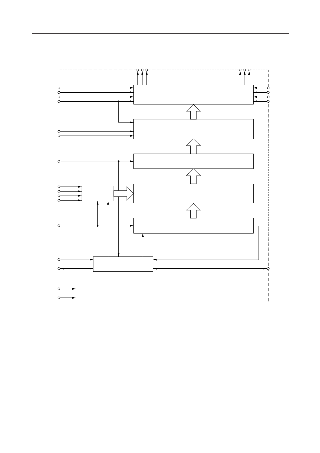
BLOCK DIAGRAM
PEDL6779B-01
MSM6779B¡ Semiconductor
V
V
V
V
EEL
DF
DISPOFF
LOAD
D
D
D
D
SHL
O3O2O
1
1L
3L
4L
160-DOT 4-LEVEL DRIVER
O
158
160-bit LEVEL SHIFTER
O
O
160
159
V
1R
V
3R
V
4R
V
EER
V
DD
´
V
EE
V
DD
´
V
SS
160-bit LATCH (II)
0
1
2
3
DATA
CONTROL
160-bit LATCH (I) (4X40)
20-bit SHIFT REGISTER
EIO
V
V
CP
DD
SS
CONTROL
1
CIRCUIT
EIO
2
2/9
Page 3
PIN CONFIGURATION (TOP VIEW)
V
1R
V
3R
V
4R
V
EER
V
DDR
SHL
V
SS
EIO
2
D
0
D
1
D
2
D
3
CP
LOAD
DF
DISPOFF
EIO
1
V
DDL
V
EEL
V
4L
V
3L
V
1L
PEDL6779B-01
MSM6779B¡ Semiconductor
O
160
O
159
O
158
O
3
O
2
O
1
Note: The drawing shown does not specify the exact outline of the TCP; it only specifies the pin
layout.
3/9
Page 4

PEDL6779B-01
MSM6779B¡ Semiconductor
ABSOLUTE MAXIMUM RATINGS
Parameter Symbol Condition Rating Unit
Supply Voltage (1) V
Supply Voltage (2) V
Input Voltage V
Storage Temperature T
*1 V1>V3>V4>VEE, V
V1=V1L=V
1R, V3=V3L=V3R
DD≥V1>V3≥VDD
DD
*1
V
DD
–
EE
I
STG
–10 V, V
, V4=V4L=V4R, VEE=V
Ta=25˚C –0.3 to 6.5 V
Ta=25˚C 0 to 30 V
Ta=25˚C –0.3 to V
—
+10 V≥V
EE
4>VEE
EEL=VEER
–30 to +85 ˚C
0.3 V
DD
+
RECOMMENDED OPERATING CONDITIONS
Parameter Symbol Condition Range Unit
Supply Voltage (1) V
Supply Voltage (2) V
DD
DD
*1
V
–
EE
Operating Temperature Top — –20 to +75 ˚C
— 2.7 to 5.5 V
— 14 to 28 V
*1 V1>V3>V4>VEE, V
DD≥V1>V3≥VDD
V1=V1L=V1R, V3=V3L=V3R, V4=V4L=V4R, VEE=V
–7 V, V
+7 V≥V
EE
4>VEE
EEL=VEER
Note: Unlike mold packages, TCP has a low light resistance. Therefore,
they are protected from light.
4/9
Page 5

ELECTRICAL CHARACTERISTICS
DC Characteristics
Parameter Symbol Condition Min. Typ. Max. Unit
"H" level Input Voltage V
"L" level Input Voltage V
"H" level Input Current I
"L" level Input Current I
"H" level output Voltage V
"L" level output Voltage V
ON Resistance R
Stand-by Current Consumption I
Current Consumption (1) I
Current Consumption (2) I
Current Consumption (3) I
Input Capacitance C
IH
IL
IH
IL
OHIO
OL
ON
DD
SBY
DD
EE
V
I
VI=VDD, VDD=5.5 V
VI=0 V, VDD=5.5 V
IO=0.2 mA, VDD=2.7 V
VDD–VEE=25 V,
V
I V
f
CP
V
No load
fCP=6.5 MHz, VDD=3.0 V
V
No load
fCP=6.5 MHz, VDD=3.0 V
V
No load
fCP=6.5 MHz, VDD=3.0 V
V
No load
f=1 MHz — 5 — pF
*1
—
*1
—
*1
=–0.2 mA, VDD=2.7 V
=2.7 V,
DD
N–VO
=0.25 V
I
*3 *4
=6.5 MHz, VDD=3.0 V
=25 V,
DD–VEE
*5
, f
=21.6kHz
LOAD
=25 V,
DD–VEE
*6
, f
=21.6kHz
LOAD
=25 V,
DD–VEE
*7
, f
=21.6kHz
LOAD
=25 V,
DD–VEE
*8
, f
=21.6kHz
LOAD
PEDL6779B-01
MSM6779B¡ Semiconductor
(V
2.7 V to 5.5 V, Ta=–20 to +75˚C)
DD
=
0.8 V
DD
— — 0.2 V
*1
—— 1mA
——–1mA
*2
*2
VDD–0.4 — — V
— — 0.4 V
— 1.5 3.0 kW
— — 300 mA
— — 1.5 mA
— — 2.0 mA
——±200 mA
——V
V
DD
*1 Applicable to LOAD, CP, D0~D3, EIO1, EIO2, SHL, DF, DISPOFF pins
*2 Applicable to EIO
*3 V
N=VDD
to VEE, V4=14/16 (VDD–VEE), V3=2/16 (VDD–VEE), VDD=V
*4 Applicable to O1 to O
*5 Display data 1010.....f
, EIO2 pins
1
1
pins
160
= 45 Hz, Current from VDD to VSS when the display data is not
DF
fetching.
*6 Display data 1010.....f
= 45 Hz, Current from VDD to VSS when the display data is
DF
fetching.
*7 Display data 1010.....f
= 45 Hz, Current from VDD to V
DF
EE
*8 Display data 1010.....fDF = 45 Hz, Current on V1, V3, and V4 pins.
V
1=VIL=VIR
, V3=V3L=V3R, V4=V4L=V4R, VEE=V
EEL=VEER
Note: The above values are quaranteed when TCP is protected from light.
5/9
Page 6

Switching Characteristics
(V
=2.7V to 5.5 V, Ta=–20 to +75˚C)
DD
Parameter Symbol Condition Min. Typ. Max. Unit
Clock Frequency f
Clock Pulse Width t
Load Pulse Width t
Clock Pulse Rise/Fall Time t
Data Set-up Time t
Data Hold Time t
Clock Load Time 1 t
Clock Load Time 2 t
Load Clock Time 1 t
Load Clock Time 2 t
Propagation Delay Time t
, EIO2 Set-up Time t
EIO
1
, EIO2 Hold Time t
EIO
1
CP
W1
W2
, t
r
f
DSU
DHD
CL1
CL2
LC1
LC2
CL=15 pF — — 236 ns
PHL
ESU
EHD
DUTY=50% — — 6.5 MHz
— 56——ns
— 70——ns
— ——20ns
— 50——ns
— 40——ns
—0——ns
— 65——ns
— 65——ns
— 65——ns
— 50——ns
— 50——ns
Note: The above values are quaranteed when TCP is protected from light.
PEDL6779B-01
MSM6779B¡ Semiconductor
D0~D
LOAD
LOAD
CP
CP
t
t
W1
0.8 V
DD
t
DSU
0.8 V
3
t
CL1
0.2 V
DD
DD
1
f
t
W1
0.8 V
DD
0.2 V
DD
t
DHD
t
LC2
t
CL2
0.8 V
DD
0.2 V
DD
t
W2
t
r
2 38 39 40 41
0.2 V
0.2 V
DD
t
r
0.8 V
0.8 V
0.2 V
t
f
DD
DD
DD
DD
t
t
W1
LC1
0.8 V
0.8 V
0.2 V
DD
DD
DD
EIO1, EIO2 (Output)
EIO1, EIO2 (Input)
t
PHL
0.2 V
0.2 V
DD
DD
t
ESU
t
EHD
0.2 V
DD
6/9
Page 7

FUNCTIONAL DESCRIPTION
Pin Descriptions
VDD, V
SS
Power supply for the device. VDD is set to 2.7 V to 5.5 V. VSS is set to 0 V.
PEDL6779B-01
MSM6779B¡ Semiconductor
V1L, V1R, V3L, V3R, V4L, V4R, V
EEL
, V
EER
Bias power supply for the LCD drive voltages. Power supply should be
V
DD≥V1>V3>V4>VEE
.
DISPOFF
Input for controlling the output level of O1 to O
. The V1 level is output from O1 to O
160
160
pins
during "L" level input. Refer to Truth Table.
DF
Input for LCD drive wave form AC synchronization.
O1~O
160
LCD drive outputs that correspond to each bit of the latch (II). Depending on the combination
of the contents of the latch (display data) and DF signal, one of 4 levels (V1, V3, V4, VEE) is output.
Refer to Truth Table.
CP
Clock pulse input for display data reading. Data is taken into the latch (I) at the falling edge of
the clock pulse.
Use an even number for the clock number per line (the number of the clock pulses during the
period from Load input to the next Load input).
EIO1, EIO
2
Chip Select Signal Input/Output. Input/Output are controlled by the SHL input. If the SHL
input at "L"level,EIO1 is output and EIO2 is input. If the SHL input is at "H" level,EIO1 is input
and EIO2 is output. If the SHL is at "L" level, the first EIO2 is fixed to "L"level,and the following
EIO2 is connected to the preceding EIO1. If the SHL is at "H"level,the first EIO1 is fixed to "L" level,
and the following EIO1 is connected to the preceding EIO2 as shown below.
When SHL is at "L" level
Start data
O
160
EIO
2
When SHL is at "H" level
End data
O
160
EIO
EIO
End data
O
1
EIO
2
EIO
1
EIO
2
1
Start data
O
1
1
EIO
2
EIO
1
EIO
2
EIO
1
7/9
Page 8

PEDL6779B-01
MSM6779B¡ Semiconductor
D0, D1, D2, D
3
These are display data inputs that input data with clock synchronization. The table below shows
the relationship between the LCD output for the display data and DFs and the LCD.
Display Data DF
LCD drive output
L L OFFNon-selection level (V3)
HL ONSelection level (V1)
L H OFFNon-selection level (V4)
HH ONSelection level (VEE)
LCD
LOAD
This is an input to simultaneously output the display data of one line stored in the latch (I). At
the falling edge, the data in the latch (I) is transferred to the latch (II) end is output.
SHL
Input to select for display data reading direction. Input of "L" level at Vss level fetches data in
the direction from O
direction from O1 to O
outputs (O1 to O
EIO
EIO
SHL
1
InputsOutputsL
OutputsInputsH
to O1 sequentially, while input of "H" level at VDD fetches data in the
160
. The table below shows the relationship between read data and driver
160
).
160
2
Data
input
40 clocks 39 clocks 38 clocks
D
0
D
1
D
2
D
3
D
0
D
1
D
2
D
3
O
1
O
2
O
3
O
4
O
160
O
159
O
158
O
157
Numbers of the clock pulse
O
5
O
6
O
7
O
8
O
156
O
155
O
154
O
153
O
9
O
10
O
11
O
12
O
152
O
151
O
150
O
149
...
3 clocks 2 clocks 1 clocks
...
...
...
...
...
...
...
...
O
149
O
150
O
151
O
152
O
12
O
11
O
10
O
9
O
153
O
154
O
155
O
156
O
8
O
7
O
6
O
5
O
157
O
158
O
159
O
160
O
4
O
3
O
2
O
1
TRUTH TABLE
DF Display Data DISPOFF Driver output (01~0
LLH V
LHH V
HLH V
HHH V
XXL V
X : don't care
NOTES ON USAGE (when turning the power ON or OFF)
If a high voltage is applied to a LCD drive system while the logic supply is floating, over
destroy the device, because the voltage over the LCD drive system is high.
Follow the sequence below when turning the power ON or OFF.
Power ON : Logic system ON Æ LCD drive system ON, or both ON
Power OFF : LCD drive system OFF Æ logic system OFF, or both OFF
3
1
4
EE
1
-current may
160
)
8/9
Page 9

PEDL6779B-01
MSM6779B¡ Semiconductor
NOTICE
1. The information contained herein can change without notice owing to product and/or
technical improvements. Before using the product, please make sure that the information
being referred to is up-to-date.
2. The outline of action and examples for application circuits described herein have been
chosen as an explanation for the standard action and performance of the product. When
planning to use the product, please ensure that the external conditions are reflected in the
actual circuit, assembly, and program designs.
3. When designing your product, please use our product below the specified maximum
ratings and within the specified operating ranges including, but not limited to, operating
voltage, power dissipation, and operating temperature.
4. Oki assumes no responsibility or liability whatsoever for any failure or unusual or
unexpected operation resulting from misuse, neglect, improper installation, repair, alteration
or accident, improper handling, or unusual physical or electrical stress including, but not
limited to, exposure to parameters beyond the specified maximum ratings or operation
outside the specified operating range.
5. Neither indemnity against nor license of a third party’s industrial and intellectual property
right, etc. is granted by us in connection with the use of the product and/or the information
and drawings contained herein. No responsibility is assumed by us for any infringement
of a third party’s right which may result from the use thereof.
6. The products listed in this document are intended for use in general electronics equipment
for commercial applications (e.g., office automation, communication equipment,
measurement equipment, consumer electronics, etc.). These products are not authorized
for use in any system or application that requires special or enhanced quality and reliability
characteristics nor in any system or application where the failure of such system or
application may result in the loss or damage of property, or death or injury to humans.
Such applications include, but are not limited to, traffic and automotive equipment, safety
devices, aerospace equipment, nuclear power control, medical equipment, and life-support
systems.
7. Certain products in this document may need government approval before they can be
exported to particular countries. The purchaser assumes the responsibility of determining
the legality of export of these products and will take appropriate and necessary steps at their
own expense for these.
8. No part of the contents contained herein may be reprinted or reproduced without our prior
permission.
9. MS-DOS is a registered trademark of Microsoft Corporation.
Copyright 2000 Oki Electric Industry Co., Ltd.
Printed in Japan
9/9
 Loading...