

Page 1

E2B0012-27-Y2
¡ Semiconductor MSM6775
¡ Semiconductor
This version: Nov. 1997
Previous version: Mar. 1996
MSM6775
1/3, 1/4, 1/5 DUTY LCD DRIVER WITH 5-DOT COMMON DRIVER AND 80-DOT
SEGMENT DRIVER
GENERAL DESCRIPTION
The MSM6775 is an LCD driver for dynamic display providing 3-duty-switchable pins (1/3, 1/
4 and 1/5 duty). It can directly drive LCDs of up to 400, 320 and 240 segments when 1/5, 1/4
and 1/3 duty are selected, respectively.
FEATURES
• Operating range
Supply voltage (VDD) : 2.7 to 5.5V
Operating temperature (T
LCD driving voltage (VDD-V
• Segment output : 80 pins
1/5 duty : Up to 400 segments can be displayed.
1/4 duty : Up to 320 segments can be displayed.
1/3 duty : Up to 240 segments can be displayed.
• Serial transfer clock frequency : 4MHz
• Serial interface with CPU : Through three input pins (DATA, LOAD, and
• One-to-one corresponcence between input data and its output
When input data is at "H" level : Display goes on.
When input data is at "L" level : Display goes off.
• Built-in oscillator circuit for COMMON signals
• The entire display can be turned off. (BLANK pin)
• Package:
100-pin plastic TQFP (TQFP100-P-1414-0.50-K) (Product name : MSM6775TS-K)
) : –40 to +85°C
op
) : 3.5 to 5.5V
LC3
CLOCK)
1/13
Page 2
¡ Semiconductor MSM6775
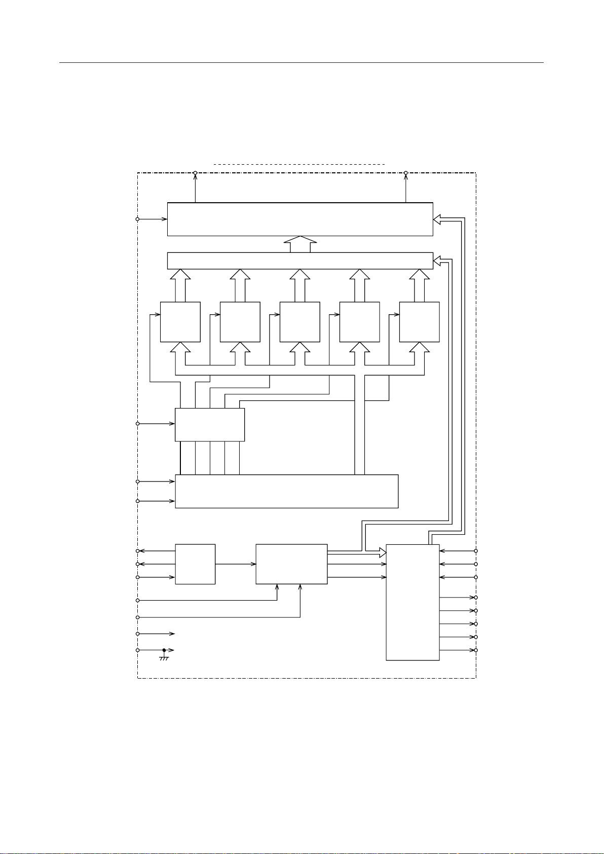
BLOCK DIAGRAM
SEG1 SEG80
BLANK
LOAD
DATA
CLOCK
80-BIT
LATCH 5
SELECTOR
LATCH
80-DOT SEGMENT DRIVER
80-CH DATA SELECTOR
80-BIT
LATCH 4
80-BIT
LATCH 3
88-BIT SHIFT REGISTER
80-BIT
LATCH 2
80-BIT
LATCH 1
80
OSC–R
OSC–C
OSC–IN
DSEL1
DSEL2
V
DD
V
SS
OSC
TIMING
GENERATOR
COMMON
DRIVER
V
LC1
V
LC2
V
LC3
COM1
COM2
COM3
COM4
COM5
2/13
Page 3
¡ Semiconductor MSM6775
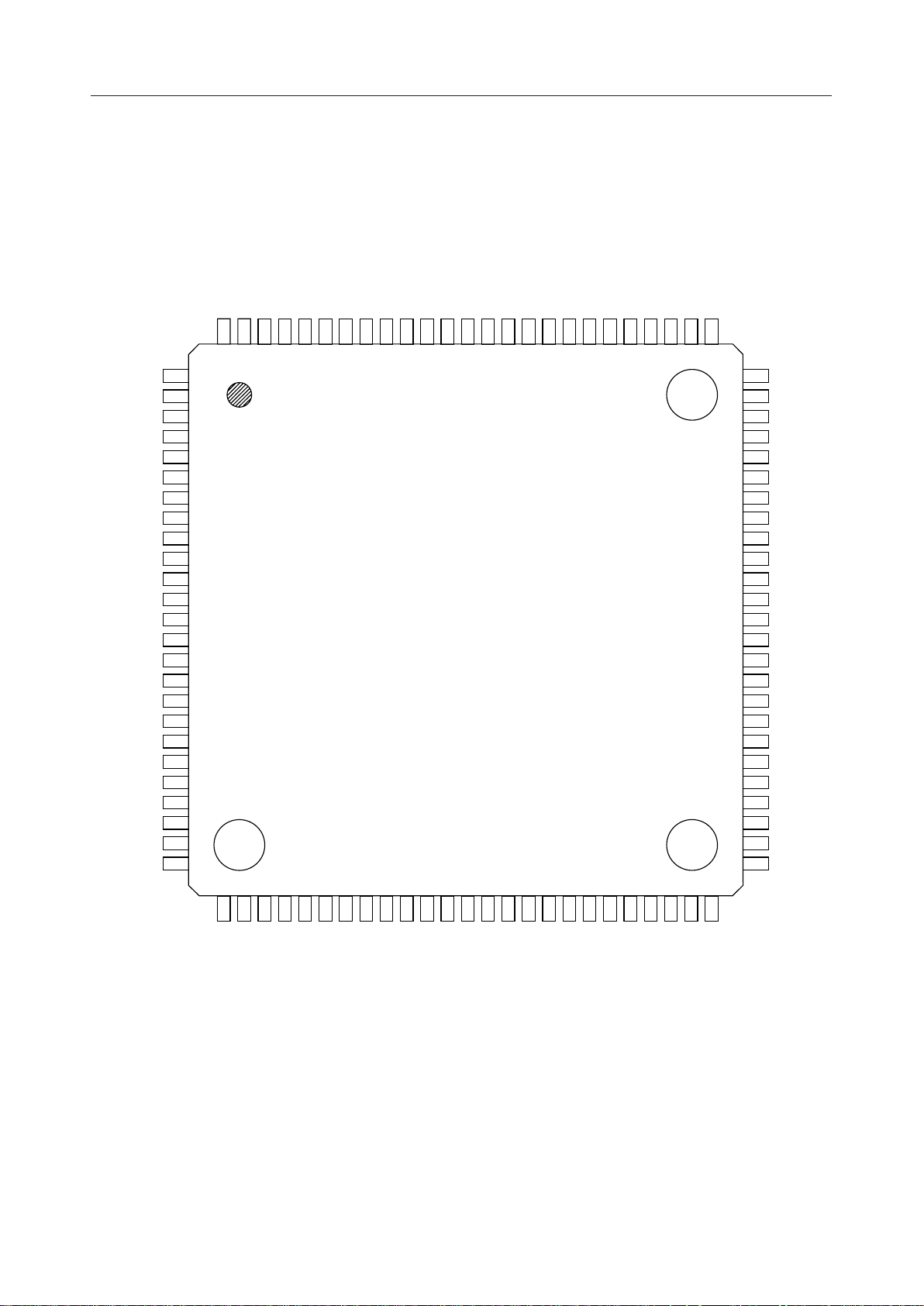
PIN CONFIGURATION (TOP VIEW)
SEG26
SEG27
SEG28
SEG29
SEG30
SEG31
SEG32
SEG33
SEG34
SEG35
SEG36
SEG37
SEG38
SEG39
SEG40
SEG41
SEG42
SEG43
SEG44
SEG45
SEG46
SEG47
SEG48
SEG49
SEG50
76
77
78
79
80
81
82
83
84
85
86
87
88
89
90
91
92
93
94
95
96
97
98
99
100
SEG51
1
2SEG52
3SEG53
4SEG54
5SEG55
6SEG56
7SEG57
8SEG58
9SEG59
10SEG60
11SEG61
12SEG62
13SEG63
14SEG64
15SEG65
16SEG66
17SEG67
18SEG68
19SEG69
20SEG70
21SEG71
22SEG72
23SEG73
24SEG74
25SEG75
75
74
73
72
71
70
69
68
67
66
65
64
63
62
61
60
59
58
57
56
55
54
53
52
51
SEG25
SEG24
SEG23
SEG22
SEG21
SEG20
SEG19
SEG18
SEG17
SEG16
SEG15
SEG14
SEG13
SEG12
SEG11
SEG10
SEG9
SEG8
SEG7
SEG6
SEG5
SEG4
SEG3
SEG2
SEG1
26
27
SEG77
SEG76
29
28
SEG79
SEG78
31
30
NC
SEG80
39
38
37
36
35
34
33
32
DD
V
LOAD
DATA
CLOCK
DSEL2
BLANK
OSC-R
DSEL1
NC : No connection
100-Pin Plastic TQFP
40
OSC-C
42
41
SS
V
OSC-IN
43
V
LC3
44
V
LC2
45
V
LC1
46
COM5
47
COM4
48
COM3
49
COM2
50
COM1
3/13
Page 4
¡ Semiconductor MSM6775
PIN DESCRIPTIONS
Symbol Type
OSC-IN I
OSC-C O
OSC-R O
DATA I
CLOCK I
LOAD I
BLANK I
DSEL1 I
DSEL2 I
Description
Pins for oscillation. The oscillator circuit is configured by externally connecting two
resistors and a capacitor. Make the wiring length as short as possible, because the
resistor connected to the OSC-IN pin has a higher value and the circuit is susceptible
to external noise.
Serial data input pin. The display goes on when input data is at "H" level, and it goes
off when input data is at "L" level.
Shift clock input pin. Data from the DATA pin is transferred in synchronization with the
rising edge of the shift clock. (Built-in Schmitt circuit is used.)
Load signal input pin. Serially input data is transferred to the 80-bit latch at "H" level
of this load signal, then held at "L" level.
Input pin that turns off all segments. The entire display goes off when "L" level is
applied to this pin. The display returns to the previous state when "H" level is applied.
Input pins to select 1/3, 1/4, or 1/5 duty. Following shows how each duty is selected.
DSEL2 DSEL1
L
L
H
L
H
X
Duty selected
1/3
1/4
1/5
X: Don't care
COM1 to
COM5
SEG1 to
SEG80
V
LC1
V
LC2
V
LC3
V
DD
V
SS
O
O
—
—
Display output pins for LCD. These pins are connected to the COMMON side on the
LCD panel.
Display output pins for LCD. These pins are connected to the SEGMENT side on the
LCD panel. For the correspondence between the output of these pins and input data,
see Section, "Data Structure".
Bias pins for LCD drive. Through these pins, bias voltages for the LCD
are externally supplied. The bias potential must meet the following condition:
V
DD>VLC1≥VLC2>VLC3
Supply voltage pin and ground pin.
4/13
Page 5

¡ Semiconductor MSM6775
ABSOLUTE MAXIMUM RATINGS
Parameter
Supply Voltage
Input Voltage
Storage Temperature
Symbol Condition Rating Unit
V
V
T
DD
I
STG
Ta=25°C
Ta=25°C
—
RECOMMENDED OPERATING CONDITIONS
Parameter
Supply Voltage
LCD Driving Voltage
Operating Temperature
Oscillator Circuit
Parameter
Oscillation Resistance
Oscillation Capacitance
Current Limiting Resistance
COMMON Signal Frequency
Symbol Condition Range Applicable pin
V
DD
VDD – V
T
op
LC3
—
—
—
Symbol Condition Min Max Applicable pin
R
C
R
f
COM
0
0
1
—
—
—
—
2.7 to 5.5
3.5 to 5.5
–40 to +85
20
0.00047
62
25
–0.3 to +6.0
–0.3 to V
DD
–55 to +150
120
0.01
360
250
+0.3
Unit
V
V
°C
Unit
kW
mF
kW
Hz
VDD, V
V
V
°C
V
DD
, V
LC1
LC2
—
OSC-R
OSC-C
OSC-IN
COM1 to
COM5
, V
LC3
Note: See Section, "Reference Data," for the resistor and capacitor values in the table.
RC Values in Oscillator Circuit
Parameter
Oscillation Resistance
Oscillation Capacitance
Current Limiting Resistance
Symbol 1/3 duty 1/4 duty 1/5 duty Applicable pin
R
0
C
0
R
1
68
0.001
220
51
0.001
160
43
0.001
130
Unit
kW
mF
kW
OSC-R
OSC-C
OSC-IN
Example of an oscillator circuit
MSM6775
R
0
C
0
OSC-R
OSC-C
R
1
OSC-IN
5/13
Page 6

¡ Semiconductor MSM6775
ELECTRICAL CHARACTERISTICS
DC Characteristics
(V
=2.7 to 5.5V, Ta=–40 to +85°C)
DD
Parameter
Symbol Condition Min Max
"H" Input Voltage 1
"L" Input Voltage 1
"H" Input Voltage 2
"L" Input Voltage 2 V
"H" Input Current V
"L" Input Current V
COMMON
Output Voltage
Segment
Output Voltage
Supply Current
*1
*1
*2
*2
*3
*3
*6
*7
*8
*6
*7
*8
*9
0.85V
DD
V
SS
0.8V
DD
V
SS
—
—
–1 V
DD
–1 V
LC1
V
–1
LC2
—
–1 V
DD
–1 V
LC1
–1
V
LC2
—
—
V
IH1
V
IL1
V
IH2
IL2
IH
IL
V
OC0
V
OC1
V
OC2
V
OC3
V
OS0
V
OS1
V
OS2
V
OS3
I
DD
VDD=5.5V, VI=V
DD
VDD=5.5V, VI=0V mA
IO=–100mAV
=4.0V *4
V
DD
IO=±100mAV
IO=±100mAV
IO=+100mAV
IO=–10mAV
=4.0V *5
V
DD
IO=±10mAV
IO=±10mAV
IO=+10mA
V
=5.0V, no load
DD
V
DD
0.15V
V
DD
0.2V
10
–10
—
V
LC1
LC2
LC3
—
V
LC1
LC2
V
LC3
0.5
Unit
DD
DD
mA
+1
+1 V
+1 V
+1
+1 V
–1
mA
V
V
V
V
V
*1 Applies to the CLOCK and OSC-IN.
*2 Applies to all input pins excluding the CLOCK and OSC-IN.
*3 Applies to all input pins.
*4 Applies to COM1 to COM5.
*5 Applies to SEG1 to SEG80.
*6 V
*7 V
*8 V
LC1
LC2
LC3
=3.0V
=2.0V
=1.0V
*9 R0=51kW R1=160kW C0=0.001mF
6/13
Page 7

¡ Semiconductor MSM6775
AC Characteristics
(V
=2.7 to 5.5V, Ta=–40 to +85°C)
DD
Parameter
Clock Frequency
Clock "H" Time
Clock "L" Time
Data Set-up Time t
Data Hold Time t
Load "H" Time t
Clock-to-load Time t
Load-to-clock Time t
Symbol Condition Min Max Applicable pin
f
CP
t
WHC
t
WLC
DS
DH
WHL
CL
LC
Rise time, Fall Time tr1, t
OSC-IN Input Frequency f
OSC-IN "H" Time t
OSC-IN "L" Time t
OSC
WHO
WLO
Rise Time, Fall Time tr2, t
—
—
—
—
70
70
—50
—50
— 100
— 100
— 100
f1
—50
—20kH
—
—
—20
—20 ms
f2
—
—
4.0
—
—
—
—
—
—
—
—
—
100 ns
Unit
MH
Z
ns
ns
ns
ns
ns
ns
ns
ns
Z
ms
CLOCK
DATA
CLOCK
LOAD
CLOCK
LOAD
CLOCK
OSC-IN
DATA
CLOCK
LOAD
OSC-IN
V
IH2
V
IL2
t
DS
t
WLC
V
IL1
V
IL1
1/f
CP
V
IL1
V
IH2
V
IL2
t
DH
t
r1
V
IH1
t
WHO
t
f1
V
IL1
t
WHL
V
IH2VIH2
V
IL2
t
f2
V
IH1
V
IL1
V
IL2
V
IL1
t
LC
t
WHC
V
IH1
t
CL
1/f
OSC
t
r2
V
IH1
V
IL1
t
WLO
(V
(V
IH1
IH2
=0.85V
=0.8V
DD VIL1
DD VIL2
=0.15VDD)
=0.2V
DD
)
7/13
Page 8

¡ Semiconductor MSM6775
FUNCTIONAL DESCRIPTION
Operation
As shown in "Data Structure" (next section), the display data consists of the data field
corresponding to the output for turning the segments on or off and the select field that selects
the input block of data. Data input to the DATA pin is loaded into the 88-bit shift register at the
rising edge of the CLOCK signal, transferred to the 80-bit latch while the load signal is at "H"
level, and then output via the 80-dot segment driver.
DATA
CLOCK
LOAD
Data in
display latch
D
1
D
DM1 DM2 DM3 C
80
C
1
C
2
C
3
C
4
5
1 8081828384 8586 8788
Old data
New data
8/13
Page 9

¡ Semiconductor MSM6775
(
)
(
)
(
)
Data Structure
Input data
First bit
End bit
C
5
Corresponds to SEG1
C
C
C
4
3
C1DM3 DM2 DM1 D
2
80D79
D
Corresponds to SEG80
D
5
D
4
3
D
D
2
1
Select bit
5 bits
Dummy bit
3 bits
Correspondence between select bits and COM1 to COM5
C
5
0
0
0
0
1
C
4
0
0
0
1
0
C
3
0
0
1
0
0
C
2
0
1
0
0
0
C
1
1
0
0
0
0
Display data corresponding to COM1
Display data corresponding to COM2
Display data corresponding to COM3
Display data corresponding to COM4
Display data corresponding to COM5
Notes: 1. Arbitrary data can be set for the dummy bits.
2. Select bits C1 to C5 select 80-bit latches that correspond to COM1 to COM5,
respectively. Therefore, if "1" is set for more than one select bit, data is set to all the
corresponding 80-bit latches.
Example:
If "1" is set to all the select bits C1 to C5, the display data of D1 to D80 is set to all the
80-bit latches that correspond to COM1 to COM5.
LCD display data
80 bits
Description
9/13
Page 10

¡ Semiconductor MSM6775
APPLICATION CIRCUITS
(For 1/4 duty)
1/4 DUTY
320-SEGMENT
LCD PANEL
CPU
P
O
R
+5V
DATA
CLOCK
LOAD
R
1
BLANK
V
DD
T
OSC-IN
C
0
SEG1 SEG80
MSM6775
COM1
COM2
COM3
COM4
COM5
Open
OSC-C
R
0
OSC-R
DSEL1
DSEL2
V
SS
V
LC1VLC2VLC3
BIAS CIRCUIT
10/13
Page 11

¡ Semiconductor MSM6775
REFERENCE DATA
The data shown in this section is for reference (a metal film resistor and a film capacitor are
used). Resistor and capacitor values must be determined based on experiments.
Use the following expression to convert oscillation frequency to COMMON frame frequency (or
vice versa):
f
COM=fOSC
f
COM
f
OSC
Duty : e.g., 1/4 for 1/4 duty
For example, if f
¥ Duty/16
: COMMON frame frequency
: Oscillation frequency
=100Hz at 1/5 duty, the oscillation frequency is f
COM
0.7
0.6
0.5
0.4
[mA]
DD
I
0.3
0.2
IDD vs. V
DD
Ta=25°C
R
=51kW
0
R
=160kW
1
C
=0.001mF
0
1/4 duty
=8000Hz.
OSC
0.1
0
234567
V
[V]
DD
COMMON Frame Frequency vs. V
DD
(The resistor and capacitor values used are their recommended values.)
120
Ta=25°C
1/3 duty
1/4 duty
110
1/5 duty
100
Frame Frequency [Hz]
90
80
234567
V
[V]
DD
11/13
Page 12

¡ Semiconductor MSM6775
5
10
4
10
Frequency [Hz]
1000
100
Oscillation Frequency vs. R
(VDD=3V)
0
20 30 40 50 60 70 80 90
R0 [kW]
100
=0.00047mF
C
0
=0.001mF
C
0
=0.0022mF
C
0
=0.0047mF
C
0
~
R
~
1 3R0
Ta=25°C
5
10
4
10
Frequency [Hz]
1000
100
Oscillation Frequency vs. R
(VDD=5V)
0
20 30 40 50 60 70 80 90
R0 [kW]
100
=0.00047mF
C
0
=0.001mF
C
0
=0.0022mF
C
0
=0.0047mF
C
0
~
R
~
1 3R0
Ta=25°C
12/13
Page 13

¡ Semiconductor MSM6775
PACKAGE DIMENSIONS
(Unit : mm)
TQFP100-P-1414-0.50-K
Mirror finish
Package material
Lead frame material
Pin treatment
Solder plate thickness
Package weight (g)
Epoxy resin
42 alloy
Solder plating
5 mm or more
0.55 TYP.
Notes for Mounting the Surface Mount Type Package
The SOP, QFP, TSOP, SOJ, QFJ (PLCC), SHP and BGA are surface mount type packages, which
are very susceptible to heat in reflow mounting and humidity absorbed in storage.
Therefore, before you perform reflow mounting, contact Oki’s responsible sales person for the
product name, package name, pin number, package code and desired mounting conditions
(reflow method, temperature and times).
13/13
 Loading...