

Page 1
4-1OKI SEMICONDUCTOR
MSM66P54
One-Time Programmable (OTP) Speech Synthesizer
DESCRIPTION
The MSM66P54 is a one-time-programmable (OTP) version of the MSM6654 speech synthesizer, suitable
for evaluation of the MSM6650 family and code development. This part is also suitable for applications
requiring small quantities and/or short-term delivery after code completion. The PC-based AR76-202
Speech Development System is used for speech encoding, editing, and programming of the MSM66P54.
When compared to the mask-programmed MSM6654 version, the SOP-packaged version of the
MSM66P54 is backwards compatible, while the DIP-packaged version has two extra pins for programming. On the DIP version, programming pins can either be cut off or left open after programming. DIP
pin spacing and location allows insertion of the MSM66P54 into an IC socket intended for the MSM6654.
To provide high-quality speech synthesis, all members of the MSM6650 family members implement
adaptive differential pulse-code modulation (ADPCM) playback, pulse-code modulation (PCM) playback, 12-bit D/A conversion, and an on-chip -40dB/octave low-pass filter (LPF). In addition, easy-to-use
“beep” tones, a two-channel mixing function, a melody function, a fade-out function, and a random playback function are included. Also, an on-chip edit ROM can form sentences by catenating phrases, making
external control simpler than before.
Four code versions of the MSM66P54 are available. Stand-alone or microcomputer (MCU) interface
modes can be selected by using one of the four available codes. The table below shows the code versions
available.
FEATURES
MSM66P54 Code Versions
Part No. OTP ROM Mode Interface/Standby Features
MSM66P54-01 1 Mbit MCU Interface Mode Serial Interface
MSM66P54-02 1 Mbit MCU Interface Mode Parallel Interface
MSM66P54-03 1 Mbit Standalone Mode Standby Function
MSM66P54-04 1 Mbit Standalone Mode No Standby Function
• Single-chip synthesizer
• 4-bit ADPCM or 8-bit PCM sound playback
• Melody function
• Edit ROM function
• Built-in two-channel mixing function
• Internal random playback function
• Fade-out function
• Built-in “beep” tones at 0.5, 1.0, 1.6, and 2.0 kHz
• Sampling frequency of 4.0, 5.3, 6.4, 8.0, 10.6, 12.8, 16, or
32 kHz
[1]
• Up to 127 phrases
• Internal 12-bit D/A converter
• Internal -40 dB/octave low-pass filter (LPF)
• Built-in standby function
• Selectable RC oscillation or ceramic/crystal
oscillation
• Package options include 20-pin DIP (DIP20-P-300),
24-pin SOP (SOP24-P-430-2K), or die
1. 32 kHz is not available when RC oscillation is selected
Page 2
■
MSM66P54 OTP Speech Synthesizer ■––––––––––––––––––––––––––––––––––––––––––––––––––––––––––
4-2 OKI SEMICONDUCTOR
The table below shows the additional functions available in the MSM6650 family when compared to the
family’s predecessor, the MSM637x family.
SPEECH DURATION
[1] Actual ROM area in MSM6652, MSM6653, MSM6654, MSM6655, and MSM6656 is smaller by 22 Kbits.
[2] Via external ROM only (no on-chip ROM available).
[3] OTP version.
Comparison of MSM6376 and MSM6650 Families
MSM6650 Family MSM637x Family
Control Method
Standalone mode
Microcomputer mode - parallel input
Microcomputer mode - serial input
CPU input - software control
Speech synthesis method
4-bit ADPCM or
8-bit PCM/Melody PCM
4-bit ADPCM
“Beep” tone frequency (length)
0.5, 1.0, 1.6, or 2.0 kHz
(User-specified length of variable duration)
1.0 or 2.0 kHz, (User-specified length,
fixed at either 64, 128, 250, or 500 ms)
Sampling frequency (fS)
Eight frequencies
(4.0, 5.3, 6.4, 8.0, 10.6, 12.8, 16.0, or 32.0 kHz)
Three frequencies at two oscillator frequencies
(4.0, 6.4, or 8.0 kHz with f
OSC
= 64 kHz;
16.0, 25.6, or 32.0 kHz with f
OSC
= 256 kHz)
Master clock frequency 256 kHz (RC) / 4.096 MHz (crystal) 40 kHz ~ 256 kHz
LPF attenuation factor –40 dB/octave –24 dB/octave
LPF cut-off Frequency (f
CUT
), kHz
Maximum phrase number 127 (in MCU Interface Mode) 111
Pull-up/pull-down resistors Built in —
Standby conversion time 200 ms 3 Sec
Maximum external ROM 64 Mbit 16 Mbit
Added functions in edit ROM
Fade-out
Random playback
Melody playback
PCM playback
Serial input control
No Edit ROM
Type
Data ROM
Capacity
[1]
Maximum Speech Duration
f
SAM
= 4.0 kHz f
SAM
= 6.4 kHz f
SAM
= 8.0 kHz f
SAM
= 16.0 kHz f
SAM
= 32.0 kHz
MSM6650 64 Mbits
[2]
> 1 hour > 40 minutes > 30 minutes > 15 minutes > 8 minutes
MSM6652 288 Kbit 16.9 sec 10.5 sec 8.4 sec 4.2 sec 2.1 sec
MSM6653 544 Kbit 31.2 sec 19.5 sec 15.6 sec 7.8 sec 3.9 sec
MSM6654 1 Mbit 63.8 sec 39.9 sec 31.9 sec 15.9 sec 7.9 sec
MSM66P54
[3]
1 Mbit 63.8 sec 39.9 sec 31.9 sec 15.9 sec 7.9 sec
MSM6655 1.5 Mbit 96.5 sec 60.3 sec 48.2 sec 24.1 sec 12.0 sec
MSM6656 2 Mbit 129.1 sec 80.7 sec 64.5 sec 32.2 sec 16.1 sec
f
CUT
1.8 2.6 2.6 3.2 4.2 5.1 6.4 12.8
f
SAM
4.0 5.3 6.4 8.0 10.6 12.8 16.0 32.0
f
CUT
1.5 3.0 3.0
f
SAM
4.0 6.4 8.0
Page 3
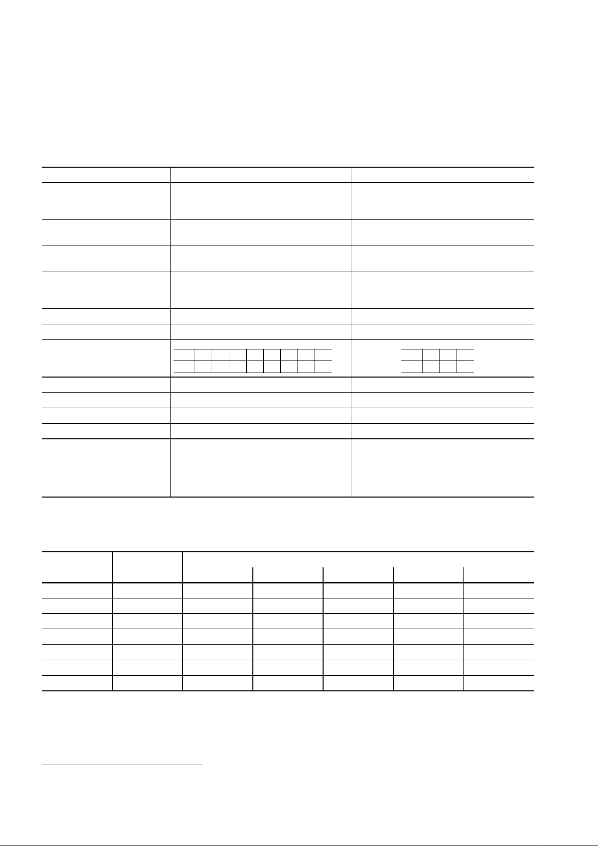
–––––––––––––––––––––––––––––––––––––––––––––––––––––––––––––––––––––––– ■ Package Drawings
■
4-3OKI SEMICONDUCTOR
PACKAGE DRAWINGS
Figure 1. MSM66P54 Mechanical Drawing (DIP20-P-300-W1 Package)
Figure 2. MSM66P54 Mechanical Drawing (SOP24-P-430-2K Package)
7.62
0~15°
0.25 +0.11/-0.05
5.08 MAX.3.3 ±0.3
6.4 ±0.2
22.6 ±0.2
18 10
19
0.6 TYP.
4.57 MAX.
SEATING
PLANE
2.54 1.5241.14 TYP. 0.46 +0.13/-0.08 ø0.25
M
Dimensions in mm.
2.2 ±0.2
2.7 MAX.
1.2 ±0.2
24 13
112
0.99 TYP.
Dimensions in mm.
Index Mark
1.27 0.35 ±0.1 0.25
M
15.95 ±0.1
7.9 ±0.1
12.0 ±0.5
Seating Plane
7.9 ±0.1
0.2 +0.1/-0.05
0~10°
2.05 ±0.3
0 ~ 0.3
Page 4
■
MSM66P54 OTP Speech Synthesizer ■––––––––––––––––––––––––––––––––––––––––––––––––––––––––––
4-4 OKI SEMICONDUCTOR
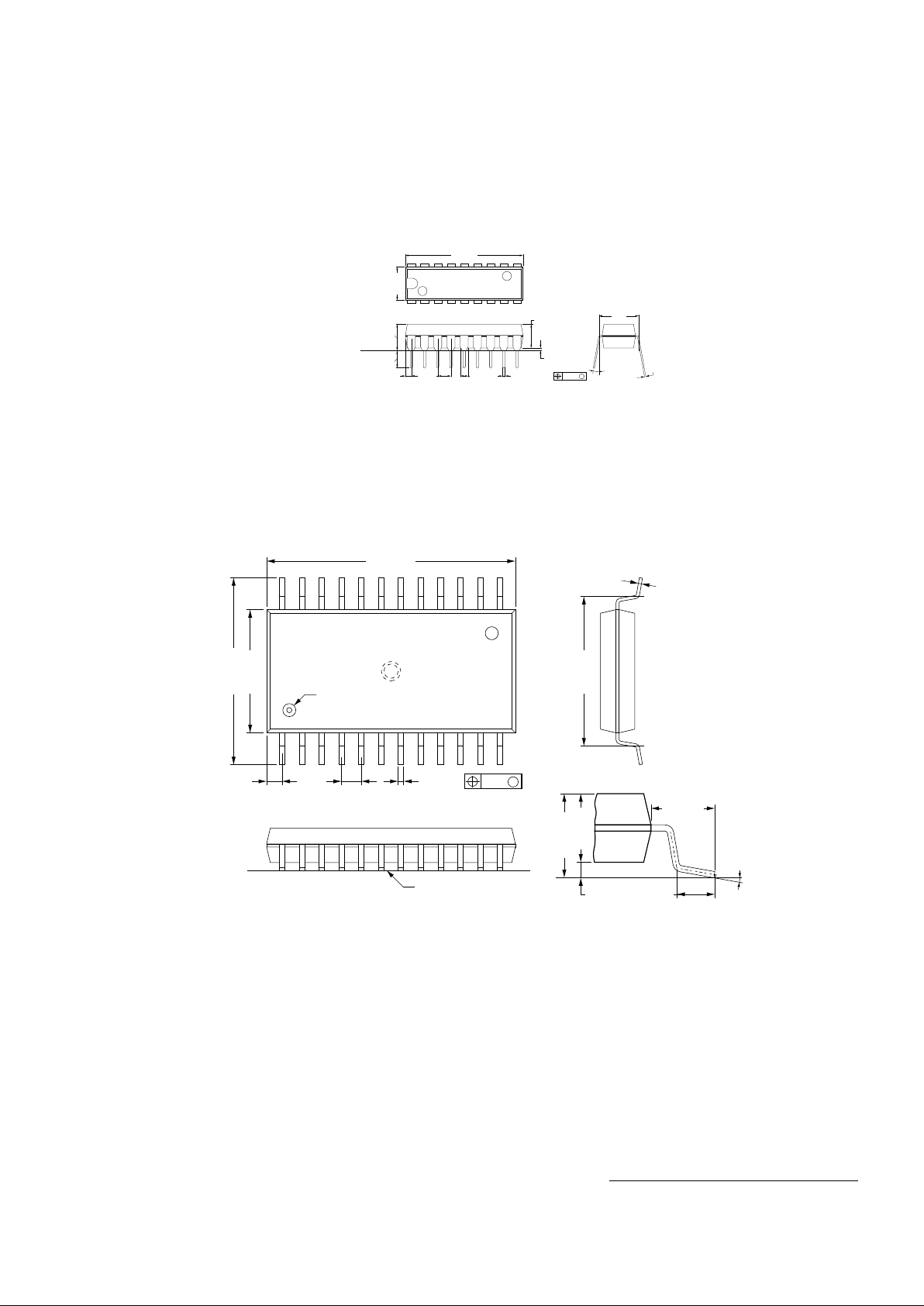
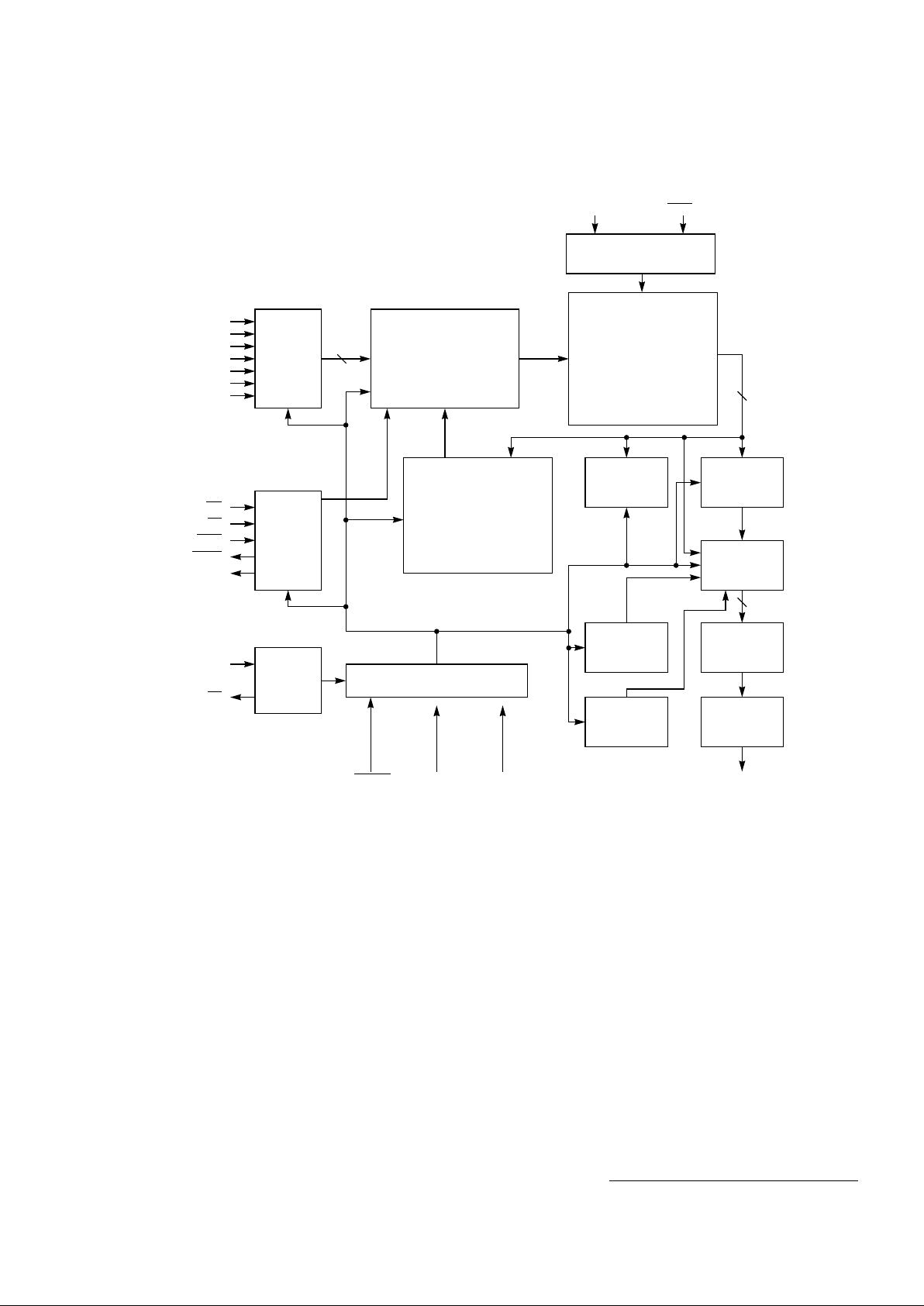
BLOCK DIAGRAMS
Figure 3. MSM66P54-03/-04 Block Diagram (Standalone Mode)
Address &
Switching
Controller
8
12
17-Stage Address Counter
7
Random
Circuit
I/O
Interface
OSC
(X’tal/RC)
Timing Controller
AOUTRESETXT/RC GNDVDD
A2
A1
A0
SW3
SW2
SW1
SW0
TEST
OSC1
OSC2
OSC3
BUSY
DATA
Controller
Melody
Generator
ADPCM
Synthesizer
PCM
Synthesizer
12-bit
DAC
LPF
BEEP Tone
Generator
RND
17-Stage Multiplexer
1-Mbit OTP ROM
(Containing 22-Kbit Edit
ROM & Address ROM)
Programming Circuitry
PGM
VPP
Page 5
–––––––––––––––––––––––––––––––––––––––––––––––––––––––––––––––––––––––––– ■ Block Diagrams
■
4-5OKI SEMICONDUCTOR
Figure 4. MSM66P54-01/-02 Block Diagram (MCU Interface Mode)
Address &
Command
Controller
8
12
17-Stage Address Counter
7
I/O
Interface
OSC
X’tal
Timing Controller
AOUTRESET GNDVDD
I6/SD
I5/SI
14
I3/PORT1
I4/PORT0
I1
I0
XT
BUSY
DATA
Controller
Melody
Generator
ADPCM
Synthesizer
PCM
Synthesizer
12-bit
DAC
LPF
BEEP Tone
Generator
17-Stage Multiplexer
NAR
ST
CMD
CH
XT
1-Mbit OTP ROM
(Containing 22-Kbit Edit
ROM & Address ROM)
Programming Circuitry
PGM
VPP
Page 6
■
MSM66P54 OTP Speech Synthesizer ■––––––––––––––––––––––––––––––––––––––––––––––––––––––––––
4-6 OKI SEMICONDUCTOR
PIN CONFIGURATION
Figure 5. MSM66P54-03/-04 Configuration (Standalone Mode)
Figure 6. MSM66P54-01/-02 Pin Configuration (MCU Interface Mode)
A0
201
A1
2
A2
3
TEST
4
RESET
5
BUSY
6
XT/RC
7
AOUT
8
GND
9
SW319
SW218
SW117
SW016
RND15
OSC314
OSC213
OSC112
VDD
18 Lead Plastic DIP
VDD
OSC1
OSC2
NC
OSC3
NC
PGM
RND
SW0
SW1
SW2
SW3
24 Lead Plastic SOP
GND
AOUT
XT/RC
NC
BUSY
NC
VPP
RESET
TEST
A2
A1
A0
24
23
22
21
20
19
18
17
16
15
14
13
1
2
3
4
5
6
7
8
9
10
11
12
10 11
VPP PGM
I4 192
I5/SI 3
I6/SD 4
CH 5
RESET 6
BUSY 7
NAR 8
AOUT 9
GND 10
I3/PORT1
18 I2/PORT0
17 I1
16 I0
15 ST
14 CMD
13 XT
12 XT
11 VDD
20-Lead Plastic DIP
VDD
XT
XT
NC
CMD
NC
PGM
ST
I0
I1
I2/PORT0
13/PORT1
24 Lead Plastic SOP
GND
AOUT
NAR
NC
BUSY
NC
VPP
RESET
CH
I6/SD
I5/SI
I4
24
23
22
21
20
19
18
17
16
15
14
13
1
2
3
4
5
6
7
8
9
10
11
12
VPP 201 PGM
Page 7
––––––––––––––––––––––––––––––––––––––––––––––––––––––––––––––––––––––––– ■ Pin Descriptions
■
4-7OKI SEMICONDUCTOR
PIN DESCRIPTIONS
MSM66P54-03/-04 Pin Descriptions (Standalone Mode)
Pin Name I/O Function
RESET
I
Reset
. Setting this pin to “L” puts the device in standby status. At this time, oscillation stops, A
OUT
is pulled to GND,
and the device is initialized. The MSM6650 Family devices have an internal power-on reset. To operate the power-on
reset correctly, power should ramp up within 1 ms. If this is not possible, apply a RESET
pulse when power is turned
on. This pin has an internal pull-up resistor.
BUSY
O
Busy
. This pin outputs a “L” level during playback. At power-on, this pin is at “H” level.
XT/RC
I
X’tal/RC selectable pin
. Set to “H” level when using ceramic/crystal oscillation. Set to “L” level when using RC
oscillation.
A
OUT
O
Sound output
. This is the synthesized output pin of the internal low-pass filter.
GND –
Ground
.
V
DD
–
Power supply
.
OSC1 I
Oscillator 1.
This pin is a ceramic/crystal oscillator connection pin when using ceramic or crystal oscillation. This pin
is an RC connection pin when using RC oscillation. When using an external clock, use this pin as the clock input.
OSC2 O
Oscillator 2
. This pin is a ceramic/crystal oscillator connection pin when using a ceramic or crystal oscillator. This is
an RC connection pin when using RC oscillation. Leave open if using an external clock. OSC2 outputs a “L” level in
standby status.
OSC3 O
Oscillator 3.
Leave open if using a ceramic/crystal oscillator. This pin is the RC connection pin when using RC
oscillation. When RC oscillation is selected, OSC3 outputs a “H” level in standby status.
RND
I
Random Playback.
Random playback starts when the RND pin is set to a “L” level. At the fall of RND, addresses from
the random address playback circuit inside the IC are fetched. Set to a “H” level if random playback is not used. This
pin has an internal pull-up resistor.
TEST
I
Test Mode
. Set to “H” level. This pin has an internal pull-up resistor.
SW0 ~ SW3 I
Phrase Inputs.
These pins are phrase input pins corresponding to playback. If the input changes, SW0 ~ SW3 pins
capture address data after 16 ms and speech playback commences. These pins have internal pull-down resistors.
A0 ~ A2 I
Phrase Inputs.
Phrase input pins corresponding to playback. The A0 input becomes invalid when the random playback
function is used.
VPP – Power-supply voltage for programming the on-chip OTP ROM. Set to a “H” level or open during normal operation.
PGM I Interface pin for AR76-202 Speech Development System. Set to a “L” level or open during normal operation. This pin
has an internal pull-down resistor.
MSM66P54-01/-02 Pin Descriptions (Microcomputer Interface Mode)
Pin Name I/O Function
RESET
I
Reset
. Setting this pin to “L” puts the device in standby status. At this time, oscillation stops, A
OUT
is pulled to GND,
and the device is initialized. The MSM6650 Family devices have an internal power-on reset. To operate the power-on
reset correctly, power should ramp up within 1 ms. If this is not possible, apply a RESET
pulse when power is turned
on. This pin has an internal pull-up resistor.
BUSY
O
Busy
. This pin outputs a “L” level during playback. At power-on, this pin is at “H” level.
NAR O
Next Address Request.
The CMD
and ST input is valid when NAR is at a “H” level. When the CH pin is at “H” level,
NAR becomes a Channel 1 status signal. When the CH
pin is at “L”, NAR becomes a Channel 2 status signal. This pin
indicates whether the register that latches the addresses of I0~I6 in the Address & Command Controller (refer to the
block diagram) is empty or not. At “H” level, it is empty and new address data may be applied. At power-on, NAR is
“H” level.
AOUT O
Analog Sound Output
. Either the D/A converter or the low-pass filter output can be selected by a command input.
GND –
Ground.
Page 8

■
MSM66P54 OTP Speech Synthesizer ■––––––––––––––––––––––––––––––––––––––––––––––––––––––––––
4-8 OKI SEMICONDUCTOR
V
DD
–
Power supply.
XT I
Ceramic/Crystal Oscillator Input.
A feedback resistor of 0.5~5M Ω between XT and XT
is built in this pin. When using
an external clock, input to this pin.
XT
O
Ceramic/Crystal Oscillator Output
. When using an external clock, leave this pin open.
CMD
I
Command Input and Option Selection Control
. Command and option input is enabled if the ST pin is set to a “L” level
when the CMD
pin is “L.” Set the CMD pin to a “H” level when CMD is not used and when using the serial input
interface. This pin has an internal pull-up resistor.
ST
I
Start
. Speech synthesis starts with the fall of ST. With the rise of ST, addresses I0~I6 are latched inside the IC. Input
ST
when the NAR status signal for Channels 1 and 2 is at a “H” level. A pull-up resistor is built into this pin.
CH
I
Channel control signal
. Channel 1 is selected at “H” level and Channel 2 is selected at “L” level. A pull-up resistor is
built into this pin.
I6/SD I
Command Input 6/Serial Data Input.
When the parallel input option is selected, this is a command and phrase input
pin. When the serial input option is selected, this pin becomes a serial data (command and address) input pin.
I5/SI I
Command Input 5/Serial Clock Input
. When the parallel input option is selected, this is a command and phrase input
pin. When the serial input option is selected, this pin becomes a serial clock input pin.
I4 I
Command Input 4.
When the parallel input option is selected, this is a command and phrase input pin. When the serial
input option is selected, leave this pin at a “L” level. A pull-up resistor is built into this pin.
I3/PORT1 I/O
Command Input 3/Port 1 Output.
When the parallel input option is selected, this is a command and phrase input pin.
When the serial input option is selected, this pin becomes a port output pin. The output from this port can be varied
by command inputs from the microcomputer interface.
I2/PORT0 I/O
Command Input 2/Port 0 Output.
When the parallel input option is selected, this is a command and phrase input pin.
When the serial input option is selected, this pin becomes a port output pin. The output from this port can be varied
by command inputs from the microcomputer interface.
I0, I1 I
Command Input 1/0.
These are command and user specified phrase input pins when parallel input is optionally
selected. When the serial input option is selected, leave these pins at a “L” level. A pull-up resistor is built into these
inputs.
VPP – Power-supply voltage for programming the on-chip OTP ROM. Set to a “H” level or open during normal operation.
PGM
I Interface pin for AR76-202 Speech Development System. Set to a “L” level or open during normal operation. This pin
has an internal pull-down resistor.
MSM66P54-01/-02 Pin Descriptions (Microcomputer Interface Mode) (Continued)
Page 9

––––––––––––––––––––––––––––––––––––––––––––––––––––––––––––––– ■ Application Circuit Examples
■
4-9OKI SEMICONDUCTOR
APPLICATION CIRCUIT EXAMPLES
Figure 7. Application Circuit in Standalone Mode
with Serial Input Interface
VDD
111 2 3 114 5 6 7 8 119 10 11 12 1113 14 15
AOUTSW0
SW1
SW2
SW3
XT/RC
RND
TEST
A0
A1
A2
GND
OSC1
OSC2
OSC3
Page 10

■
MSM66P54 OTP Speech Synthesizer ■––––––––––––––––––––––––––––––––––––––––––––––––––––––––––
4-10 OKI SEMICONDUCTOR
Figure 8. Application Circuit in Standalone Mode
with Parallel Input Interface
The following table shows a comparison between switches and speech playback addresses.
Switches and Speech Playback Address Comparison
A2 A1 A0 SW3 SW2 SW1 SW0 ADR
S1000000101
S2000001002
S3000010004
S4000100008
VDD
S4 S3
AOUTSW0
SW1
SW2
SW3
RND
TEST
A0
A1
A2
GND
OSC1
OSC2
OSC3
S2 S1
XT/RC
Page 11

––––––––––––––––––––––––––––––––––––––––––––––––––––––––––––––– ■ Application Circuit Examples
■
4-11OKI SEMICONDUCTOR
Figure 9. Application Circuit in MCU Interface Mode
with a Serial Input Interface
VDD
AOUT
I6/SD
I5/SI
ST
RESET
MSM6650 Family
NAR
GND
I0
I1
I4
AMP
PORT2
PORT1
I1
I4
P1.0
P1.1
P1.2
P2.0
MSM83C154
P3.0
SA
RESET
XT
XT
Page 12

■
MSM66P54 OTP Speech Synthesizer ■––––––––––––––––––––––––––––––––––––––––––––––––––––––––––
4-12 OKI SEMICONDUCTOR
Figure 10. Application Circuit in MCU Interface Mode
with a Parallel Input Interface
ELECTRICAL CHARACTERISTICS
[1] In Microcomputer Interface Mode only.
[2] The accuracy of the oscillation frequency when RC oscillation is selected depends largely on the accuracy of the R and C
of the external parts.
Absolute Maximum Ratings
Item Symbol Conditions Rating Unit
Power supply voltage V
DD
Ta = 25˚ C
-0.3 ~ 7.0 V
Input voltage V
IN
-0.3 ~ VDD+0.3 V
Storage temperature T
stg
– -55 ~ 150 ˚ C
Recommended Operating Conditions
Parameter Symbol Conditions Rated Value Unit
Power supply voltage V
DD
LPF output
+2.7 ~ +5.5
V
DAC Output
[1]
+2.4 ~ +5.5
Operating temperature T
OP
– -10 ~ 70
°
C
Original oscillation frequency 1 f
OSC
When X’tal selected 3.5 ~ 4.5 MHz
Original oscillation frequency 2 f
OSC2
When RC selected
[2]
200 ~ 300 kHz
VDD
AOUT
I6
~
CH
MSM6650 Family
GND
AMP
P1.6
P1.0
P2.0
MSM83C154
P3.1
SA
RESET
I0
CMD
ST
RESET
NAR
~
P2.2
P2.1
P3.0
XT
XT
Page 13

–––––––––––––––––––––––––––––––––––––––––––––––––––––––––––––––––– ■ Electrical Characteristics
■
4-13OKI SEMICONDUCTOR
DC Characteristics (VDD = 5.0 V, GND = 0 V, Ta = -10 ~ 70˚ C)
Item Symbol Conditions MIN TYP MAX Unit
“H” input voltage V
IH
– 4.2 – – V
“L” input voltage V
IL
– – – 0.8 V
“H” output voltage V
OH
IOH = -1 mA 4.6 – – V
“L” output voltage V
OL
I
OL
= 2 mA – – 0.4 V
“H” input current 1 I
IH1
VIH = V
DD
––10
µ
A
“H” input current 2 I
IH2
Internal pull-down resistance -200 -90 -30
µ
A
“L” input current 1 I
IL1
VIL=GND -10 – –
µ
A
“L” input current 2 I
IL2
Internal pull-up resistance 30 90 200
µ
A
Operating power consumption I
DD
––610mA
Standby power consumption I
DS
–––10
µA
LPF driving resistor R
AOUT
–50––kΩ
LPF output impedance R
LFP
IF = 100 µA –13kΩ
DC Characteristics (VDD = 3.1 V, GND = 0 V, Ta = -10 ~ 70˚ C)
Item Symbol Conditions MIN TYP MAX Unit
“H” input voltage V
IH
– 2.7 – – V
“L” input voltage V
IL
– – – 0.5 V
“H” output voltage V
OH
I
OH
= -1 mA 2.6 – – V
“L” output voltage V
OL
I
OL
= 2 mA – – 0.4 V
“H” input current 1 I
IH1
V
IH
= V
DD
––10µA
“H” input current 2 I
IH2
Internal pull-down resistance -100 -30 -10 µA
“L” input current 1 I
IL1
V
IL
= GND -10 – – µA
“L” input current 2 I
IL2
Internal pull-up resistance 10 30 100 µA
Operating power consumption I
DD
– –47mA
Standby power consumption I
DS
– ––1µA
LPF driving resistor R
AOUT
–50––kΩ
LPF output impedance R
LPF
IF = 100 µA13kΩ
AC Characteristics (Standalone Mode, V
DD
= 5.0 V, GND = 0 V, Ta = 10 ~ 70˚ C)
Item Symbol Condition MIN TYP MAX Unit
Master clock duty cycle f
duty
– 405060%
RESET
input pulse width tw
(RST)
–10––µs
RESET
input time after power-on td
(RST)
– 0––µs
RND
input pulse width tw
(RAN)
Function details 5.2 100 – – µs
SW0 ~ SW3 input pulse width tw
(SW)
–16––ms
BUSY
output time t
SBS
–––10µs
BUSY
output time t
BN
At f
SAM
= 8 kHz 350 375 400 µs
Chattering prevention time t
CHA
– 141516ms
Page 14

■ MSM66P54 OTP Speech Synthesizer ■––––––––––––––––––––––––––––––––––––––––––––––––––––––––––
4-14 OKI SEMICONDUCTOR
Timing Waveforms
Figure 11. Power-On Timing
[1] Accuracy of oscillation frequencies when selecting RC oscillation strongly depends on the accuracy of the externally installed capacitor and
resistor.
D/A converter change time t
DAR
– 606468ms
LPF stabilization time t
L
–6810ms
Standby transition period t
STB
– 0.15 0.20 0.25 sec
Random access capture time t
RA
Function details 5.2 16 32 48 µs
AC Characteristics (Microcomputer Interface Mode, V
DD
= 5.0 V, GND = 0 V, Ta = 10 ~ 70˚ C)
Item Symbol Condition MIN TYP MAX Unit
Master clock frequency (1) f
(OSC1)
At XT selection – 4.096 – MHz
Master clock frequency (2) f
(OSC2)
At RC selection
[1]
– 256 – kHz
Master clock duty cycle f
duty
– 405060%
O(RESET
) input pulse width
tw
(O(RST)) – 10 – – µs
O(RND
) input pulse width
tw
(O(RAN)) – 100 – – µs
SW0~SW3 input pulse width tw
(SW)
–32––ms
(BUSY
) output time t
SBS
–––10µs
(BUSY
) output time t
BN
At fs = 8 kHz 350 375 400 µs
(BUSY
) output time t
BF
–––64ms
Chattering prevention time t
CHA
– 293031ms
DA converter change time t
DAR
– 606468ms
LPF stabilization time t
L
–6810ms
Standby transition period t
STB
– 0.15 0.2 0.25 sec
AC Characteristics (Standalone Mode, V
DD
= 5.0 V, GND = 0 V, Ta = 10 ~ 70˚ C) (Continued)
Item Symbol Condition MIN TYP MAX Unit
V
DD
td
(RST)
tw
(RST)
RESET (I)
BUSY (O)
Page 15

–––––––––––––––––––––––––––––––––––––––––––––––––––––––––––––––––– ■ Electrical Characteristics ■
4-15OKI SEMICONDUCTOR
Figure 12. Activation of Standby State Timing
Figure 13. Repeated Playback Timing – Standalone Mode
SW0 (I)
tw
(SW)
A0UT (O)
t
CHA
t
SBS
t
L
t
DAR
t
STB
t
DAF
Standby Status
Standby Conversion Time
Speech Startup
Address Data Capture
IBUSY (O)
STANDBY (O)
BUSY(O)
Standby Status
SWO (I)
t
BN
AOUT (I)
BUSY (O)
Single-Phrase
Repeated Playback
Single
Phrase
Playback
Page 16

■ MSM66P54 OTP Speech Synthesizer ■––––––––––––––––––––––––––––––––––––––––––––––––––––––––––
4-16 OKI SEMICONDUCTOR
Figure 14. Playback Timing during Transition of SW0 ~ SW3 – Standalone Mode
Figure 15. Repeated Random Playback Timing – Standalone Mode
A0~A2 (I)
First Phrase Playback Stops
AOUT (O)
SW0~SW3 (I) “L”
SW1 (I)
BUSY (O)
First Phrase
Play
Second Phrase
Play
SW0 (I)
t
CHA
RND (I)
Speech Starts Up
AOUT (O)
BUSY (O)
Random Address Capture
Same Phrase
Repeated Playback
First Phrase
Play
Page 17

–––––––––––––––––––––––––––––––––––––––––––––––––––––––––––––––––– ■ Electrical Characteristics ■
4-17OKI SEMICONDUCTOR
Figure 16. Channel 1 Playbac k Timing with No External Commands – Microcomputer Interface
Mode with Parallel Input
1st Phrase Play
CH (I)
CMD (I)
“H”
“H”
BUSY (O)
NAR (O)
AOUT (O)
1st Phrase Address10 ~ 16 (I)
ST (I)
2nd Phrase Address 3rd Phrase Address
t
L
t
DAR
2nd Phrase Play 3rd Phrase Play
t
NAB
t
BN
t
NAC
Page 18

■ MSM66P54 OTP Speech Synthesizer ■––––––––––––––––––––––––––––––––––––––––––––––––––––––––––
4-18 OKI SEMICONDUCTOR
Figure 17. Channel 1 Playback Timing when External Commands are Used – Microcomputer
Interface Mode with Parallel Input
1st Phrase Play
CH (I)
“H”
BUSY (O)
NAR (O)
AOUT (O)
ST (I)
2nd Phrase Play
CMD (I)
1st Phrase (Address Data)10 ~ 16 (I) 2nd Phrase (Address Data)Command Data
Page 19

–––––––––––––––––––––––––––––––––––––––––––––––––––––––––––––––––– ■ Electrical Characteristics ■
4-19OKI SEMICONDUCTOR
Figure 18. Channels 1 and 2 Playback Timing when External Commands are Used –
Microcomputer Interface Mode with Parallel Input
1st Phrase Play
CH (I)
“H”
BUSY (O)
NAR (O)
AOUT (O)
ST (I)
CMD (I)
1st Phrase (Address Data)16 ~ I0 (I) 2nd PhraseCommand Data
2nd Phrase
Play
Playback in
Channel 2
3rd Phrase
Play
t
SCH
t
CHS
Command Data 3rd Phrase
Page 20

■ MSM66P54 OTP Speech Synthesizer ■––––––––––––––––––––––––––––––––––––––––––––––––––––––––––
4-20 OKI SEMICONDUCTOR
Figure 19. Playback Timing without Using External Command – Microcomputer Interface
Mode with Serial Input
During serial input, data is transferred to the IC with the rising of the ST
input
after the input of the serial data.
1st Phrase Address Serial Input
16/SD (I)
ST (I)
BUSY (0)
NAR (0)
Speech Startup
15/SI (I)
1st Phrase Play
AOUT (O)
CMD (I)
“H”
CH (I)
“H”
2nd Phrase Address Serial Input
t
SDS
t
SSD
t
SDS
t
SIS
t
SIS
t
NAC
tw
(SCK)
Page 21

–––––––––––––––––––––––––––––––––––––––––––––––––––––––––––––––––– ■ Electrical Characteristics ■
4-21OKI SEMICONDUCTOR
Figure 20. Playback Timing using External Command – Microcomputer Interface Mode with
Serial Input
Port Output
1st Phrase Address Serial InputCommand Serial Input
Silence Command Input
CH (I)
16/SD (I)
15/SI (I)
PORT1 (O)
PORT0 (O)
CMD (I)
“H”
ST (I)
“H”
BUSY (O)
NAR (O)
AOUT (O)
Speech Playback
Code Set
Speech Startup
Page 22

■ MSM66P54 OTP Speech Synthesizer ■––––––––––––––––––––––––––––––––––––––––––––––––––––––––––
4-22 OKI SEMICONDUCTOR
 Loading...