

Datasheet MSM6596A-xxxJS, MSM6596A-xxxRS, MSM6596A-xxxGS-AK, MSM6596A-xxxGS-K Datasheet (OKI)
Page 1

E2D0039-39-21
¡ Semiconductor MSM6596A-xxx
¡ Semiconductor
This version: Feb. 1999
Previous version: May. 1997
MSM6596A-xxx
2-Mbit Serial Voice ROM
GENERAL DESCRIPTION
The MSM6596A is the shorter-TAT processing version of the MSM6596.
The MSM6596A is a serial voice ROM with a 1,048,576-word ¥ 1-bit ¥ 2-bank configuration.
The MSM6596A has a built-in internal address-generating circuit. A single, external clock input
allows continuous, serial read operations. The internal addresses are automatically incremented
by 1 by read operation. 1024 words in X direction and 1024 words in Y direction can be addressed
by inputting external serial addresses. Banks are switched with CS1 and CS2.
A read and playback device with predetermined messages can easily be configured by storing the
voice data into the MSM6596A and combining it with one of OKI's recording and playback ICs and
serial register IC.
A serial register is required to drive the MSM6596A by the MSM6388 or MSM6588. (The MSM6596A
does not operate without a serial register.)
The major functional differences between the MSM6596A and MSM6596 are shown below.
MSM6596A DC Characteristics
Parameter Symbol Condition Min. Max. Unit
Current consumption (1) I
Current consumption (2) I
DD
DS
t
RDC
CS1 = CS2 =
V
– 0.2 V
DD
= 2.5 ms — 20 mA
Ta = –40
to +70°C
Ta = –40
to +85°C
Typical values are at V
= 2.7 to 5.5 V, Ta = –40 to +85°C
V
DD
Typ.
9
—
—
—
DD
10
50—
= 5.0 V, Ta = 25°C.
MSM6596 DC Characteristics
= 3.5 to 5.5 V, Ta = –40 to +85C°
V
DD
Parameter Symbol Condition Min. Max. Unit
Current consumption (1) I
Current consumption (2) I
DD
DS
t
= 2.5 ms — 15 mA
RDC
CS1 = CS2 = VDD–0.2 V — 10 mA—
Typical values are at V
Typ.
—
= 5.0 V, Ta = 25°C.
DD
For other details, refer to individual sections in this data sheet.
FEATURES
mA
• Configuration : 1,048,576 words ¥ 1 bit ¥ 2 banks
• Serial access : Read cycle time of 2.5 ms
• Shorter-TAT processing
• Power-supply voltage : 2.7 to 5.5 V
• Package options :
18-pin plastic QFJ (QFJ18-P-R290-1.27) (Product name : MSM6596A-xxxJS)
24-pin plastic SOP (SOP24-P-430-1.27-K) (Product name : MSM6596A-xxxGS-K)
18-pin plastic DIP (DIP18-P-300-2.54) (Product name : MSM6596A-xxxRS)
30-pin plastic SSOP (SSOP30-P-56-0.65-K) (Product name : MSM6596A-xxxGS-AK)
1/12
Page 2
¡ Semiconductor MSM6596A-xxx
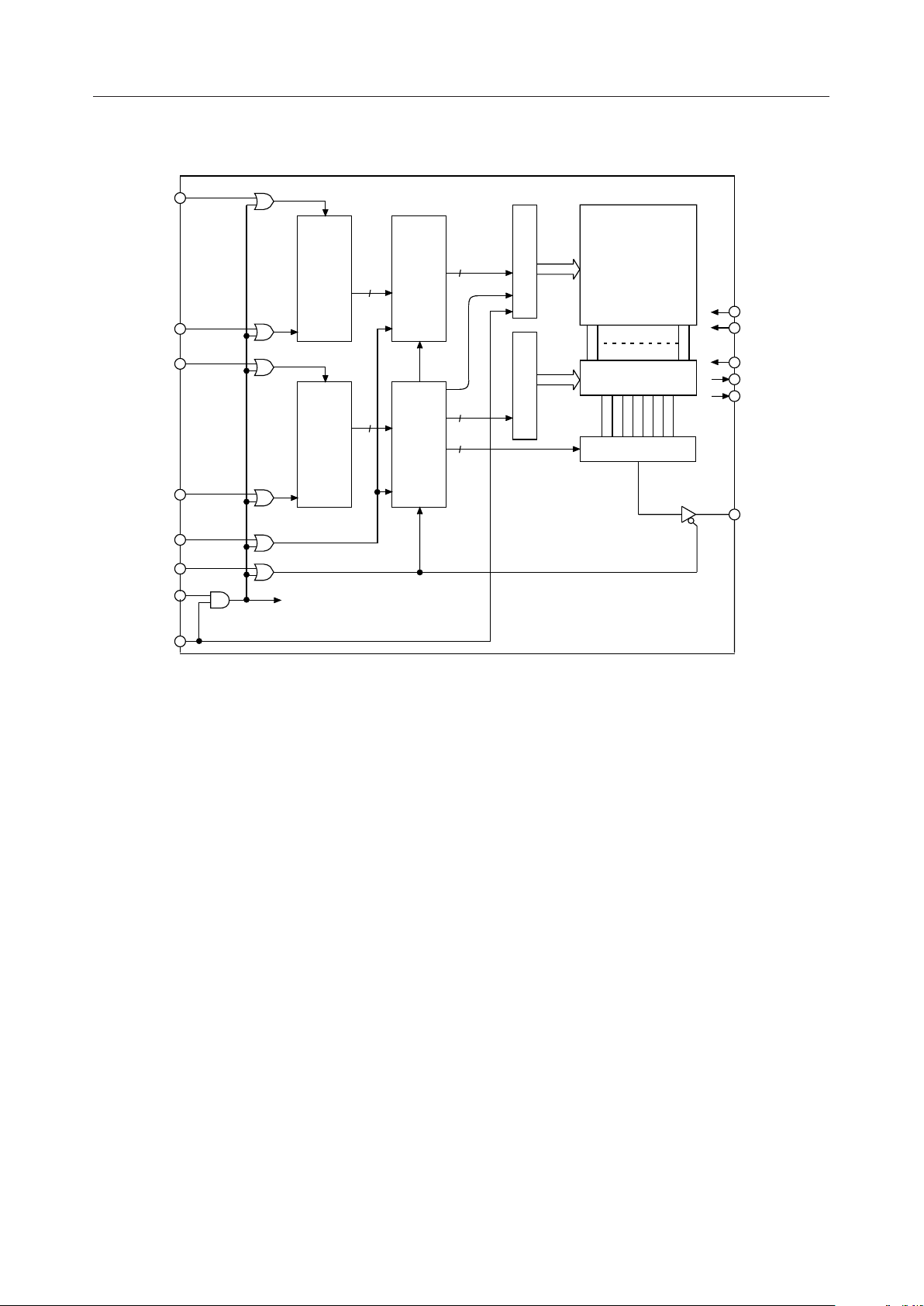
BLOCK DIAGRAM
SADX
Sin
Memory Cell
Matrix
262144 ¥ 8
V
DD
GND
SASX
X-ADDRESS
REGISTER
CK
10
X-ADDRESS
COUNTER
LD
CK
10
1
1
X-DECODERY-DECODER
SADY
SASY
TAS
RDCK
CS2
CS1
Sin
10
Y-ADDRESS
REGISTER
CK
CS CONTROL
Y-ADDRESS
COUNTER
LD
CK
TEST
MULTIPLEXER
6
3
MULTIPLEXER
TESTO1
TESTO2
DOUT
2/12
Page 3

¡ Semiconductor MSM6596A-xxx
PIN CONFIGURATIONS (TOP VIEW)
SASY
SADY
GND
DOUT
24
23
22
21
20
19
18
17
16
15
14
13
GND
NC
DOUT
TESTO1
NC
NC
NC
NC
NC
RDCK
TESTO2
TEST
CS2
CS1
NC
SADX
SASX
2 1 18 17
3
4
5
6
7
8 9 10 11
DD
TAS
V
TEST
NC: No connection
16
15
14
13
12
TESTO2
TESTO1
NC
NC
RDCK
NC
SADY
SASY
CS2
CS1
NC
NC
NC
NC
SADX
SASX
TAS
V
DD
1
2
3
4
5
6
7
8
9
10
11
12
NC: No connection
SADY
SASY
CS2
CS1
NC
SADX
SASX
TAS
V
DD
18-Pin Plastic QFJ
1
2
3
4
5
6
7
8
9
NC: No connection
18-Pin Plastic DIP
18
17
16
15
14
13
12
11
10
GND
DOUT
TESTO1
NC
NC
RDCK
NC
TESTO2
TEST
SADY
SASY
CS2
NC
CS1
NC
NC
NC
NC
NC
NC
SADX
SASX
TAS
V
DD
24-Pin Plastic SOP
1
2
3
4
5
6
7
8
9
10
11
12
13
14
15
NC: No connection
30
29
28
27
26
25
24
23
22
21
20
19
18
17
16
GND
NC
DOUT
TESTO1
NC
NC
NC
NC
NC
NC
NC
NC
RDCK
TESTO2
TEST
30-Pin Plastic SSOP
3/12
Page 4
¡ Semiconductor MSM6596A-xxx
PIN DESCRIPTIONS
18
Pin
Symbol
SSOP
DIPSOPQFJ
Type
Description
Power supply pin. Insert a bypass capacitor of 0.1 mF or more between this
9
12
24
9
18
15
30
V
DD
GND
—
pin and the GND pin.
Ground pin
—
(SERIAL ADDRESS) This pin inputs the starting X address of a read operation.
6
9
6
12
SADX
Addressing in units of 1024 words is possible. The 1024-word address data
I
can be input as 10-bit (AX0 - AX9) serial data via the SADX pin.
(SERIAL ADDRESS) This pin inputs the starting Y address of a read operation.
1
1
1
1
SADY
Addressing in units of 1024 words is possible. The 1024-word address data
I
can be input as 10-bit (AY0 - AY9) serial data via the SADY pin.
(SERIAL ADDRESS STROBE) This is the clock input pin which is used to store
7
10
7
13
SASX
I
the serial address data of the X address into the device's internal register.
(SERIAL ADDRESS STROBE) This is the clock input pin which is used to store
2
2
2
2
ISASY
the serial address data of the Y address into the device's internal register.
(TRANSFER ADDRESS STROBE) This is the input pin for loading the serial
8
11
8
14
TAS
address data into the internal address counter.
I
The X and Y addresses are stored at the falling edge of TAS.
(READ CLOCK) This is the clock input pin for reading information out of the data
13
15
13
18
RDCK
register. Internal operation starts at the falling edge of RDCK. The information
I
in the data register is output on the DOUT pin. The internal address counter is
automatically incremented at the falling edge of RDCK.
(DATA OUT) The data output pin is always kept in a high-impedance state
17
22
17
28
DOUT
when RDCK or CS is kept "H". This pin reflects the "H" or "L" level data being
O
read, and the current data is hold until ROCK is asserted "H".
(CHIP SELECT) When CS1 is set to "L", bank 1 is selected. When CS2 is set to
"L", bank 2 is selected. Setting both CS1 and CS2 to "H" disables all input and
I
output pins. These pins enable parallel use of multiple serial voice ROMs by
connecting the data output pins.
Pin for testing. Apply a "L" level.
I
Pins for testing. Leave these pins open.
O
10
16
4
4
4
CS1
5
3333 CS2
13
21
10
16
16
27
17111411
TEST
TESTO1
TESTO2
ABSOLUTE MAXIMUM RATINGS
Parameter Symbol Condition Rating Unit
Power Supply Voltage V
Input Voltage V
Storage Temperature T
DD
IN
STG
Ta = 25°C –0.3 to +7.0 V
Ta = 25°C –0.3 to VDD+0.3 V
— –55 to +150 °C
4/12
Page 5

¡ Semiconductor MSM6596A-xxx
RECOMMENDED OPERATING CONDITIONS
Parameter Symbol Condition Range Unit
Power Supply Voltage V
Operating Temperature T
DD
op
GND=0 V 2.7 to 5.5 V
— –40 to +85 °C
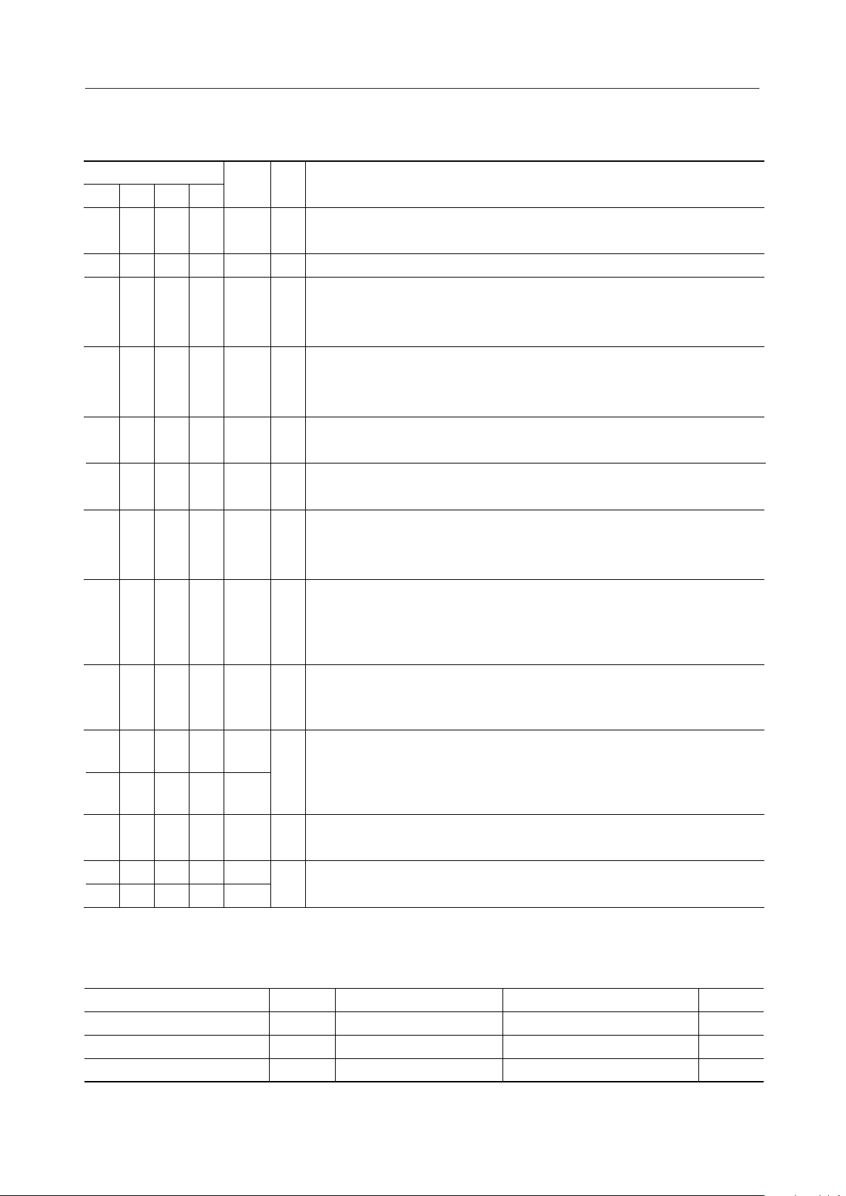
ELECTRICAL CHARACTERISTICS
DC Characteristics
= 2.7 to 5.5 V, Ta = –40 to +85°C
V
DD
Parameter Symbol Condition Min. Max. Unit
"H" Level Input Voltage V
"L" Level Input Voltage V
"H" Level Output Voltage V
"L" Level Output Voltage V
"H" Level Input Current I
"L" Level Input Current I
Current Consumption (1) I
Current Consumption (2) I
OH
OL
IH
IL
DD
DS
IH
IL
— 0.85xV
— — 0.15xV
I
= –40 mAV
OH
I
= 2 mA — 0.45 V
OL
V
= V
IH
DD
V
= GND –10 — mA
IL
t
= 2.5 ms — 20 mA
RDC
–0.3 — V
DD
—10mA
Ta = –40
CS1 = CS2 =
V
– 0.2 V
DD
to +70°C
Ta = –40
to +85°C
—
—
DD
Typ.
—
—
—
—
—
—
9
—
—V
V
DD
10
mA
50—
Typical values are at V
AC Characteristics
V
Parameter Symbol Min. Max. Unit
CS, SAS Setup Time t
SASX, SASY Cycle Time t
SASX, SASY Precharge Time t
SASX, SASY Pulse Width t
Address Setup Time t
Address Hold Time t
TAS Setup Time t
TAS, RDCK Setup Time t
TAS Pulse Width t
Read Cycle Time t
Access Time t
Output Turn-off Delay Time t
RDCK Precharge Time t
RDCK Pulse Width t
= 5.0 V, Ta = 25°C.
DD
= 2.7 to 5.5 V, Ta = –40 to +85°C
DD
CSS
SSC
SAP
SAS
AS
AH
ATS
TRS
TAS
RDC
ACC
OFF
RDP
RD
1000 — ns
500 — ns
250 — ns
250 — ns
100 — ns
100 — ns
500 — ns
500 — ns
250 — ns
2500 — ns
— 1500 ns
0 200 ns
1000 — ns
1500 — ns
5/12
Page 6

6/12
¡ Semiconductor MSM6596A-xxx
TIMING DIAGRAMS
Serial Address Input Timing
,
CS2 (I)
SADX (I)
SASX (I)
SADY (I)
t
AH
TAS (I)
SASY (I)
AX1 AX2 AX3 AX4 AX5 AX6 AX7 AX8 AX9
t
AS
t
SAS
t
CSS
t
SSC
t
SAP
t
ATS
t
ATS
t
TAS
t
AS
t
AH
t
SAS
t
SAP
t
SSC
t
CSS
AX0
AY0 AY1 AY2 AY3 AY4 AY5 AY6 AY7 AY8 AY9
,
,
,
,
,
,
CS1 (I)
Page 7

7/12
¡ Semiconductor MSM6596A-xxx
Read Access Timing
,
,
t
TAS
t
TRS
t
RDC
tRDt
RDP
t
OFF
t
ACC
XnY
m
XnY
m+1
XnY
m+2
XnY
1023
X
n+1Y0
X
n+1Y1
TAS (I)
RDCK (I)
DOUT (O)
Page 8

¡ Semiconductor MSM6596A-xxx
APPLICATION CIRCUIT
MSM6588 Playback Storage Example
MICROCONTROLLER
+
AV
DD
+
+
DVDD D V
DD'
D3
D2
D1
D0
RD
WR
CE
MCUM
TEST
RSEL1
RSEL2
TEST
TEST
TEST
TEST
RESET
MIN
MOUT
LIN
LOUT
AMON
FIN
FOUT
ADIN
SG
DGND AGND
A V
DD
SAD
SAS
TAS
RWCK
WE
DI/O
CS1
MSM6588
CS2
CS3
CS4
MON
XT
XT
AOUT
DGND
SAD
SAS
TAS
RWCK
WE
DIN
DOUT
AU/D
TEST
TEST
TEST
TEST
TEST
CS
4.096 MHz
V
DD
MSM6389
GND
Speaker amplifier
V
DD
MSM6389
1-Mbit SERIAL REGISTER
CS
GND
SADX
SASX
TAS
RDCK
DOUT
SASY
SADY
TEST
CS1
V
DD
MSM6596A-xxx
2-Mbit SERIAL VOICE ROM
CS2
GND
AGND
Note: When the MSM6596A is driven by the MSM6388 or MSM6588, a serial register is required.
(The MSM6596A does not operate without it.) The MSM6389 is being used as the serial
register in the above example.
8/12
Page 9

¡ Semiconductor MSM6596A-xxx
PACKAGE DIMENSIONS
(Unit : mm)
QFJ18-P-R290-1.27
Spherical surface
Package material
Lead frame material
Pin treatment
Solder plate thickness
Package weight (g)
Epoxy resin
42 alloy
Solder plating
5 mm or more
0.50 TYP.
Notes for Mounting the Surface Mount Type Package
The SOP, QFP, TSOP, TQFP, LQFP, SOJ, QFJ (PLCC), SHP, and BGA are surface mount type
packages, which are very susceptible to heat in reflow mounting and humidity absorbed in
storage. Therefore, before you perform reflow mounting, contact Oki’s responsible sales person
on the product name, package name, pin number, package code and desired mounting conditions
(reflow method, temperature and times).
9/12
Page 10

¡ Semiconductor MSM6596A-xxx
(Unit : mm)
SOP24-P-430-1.27-K
Mirror finish
Package material
Lead frame material
Pin treatment
Solder plate thickness
Package weight (g)
Epoxy resin
42 alloy
Solder plating
5 mm or more
0.58 TYP.
Notes for Mounting the Surface Mount Type Package
The SOP, QFP, TSOP, TQFP, LQFP, SOJ, QFJ (PLCC), SHP, and BGA are surface mount type
packages, which are very susceptible to heat in reflow mounting and humidity absorbed in
storage. Therefore, before you perform reflow mounting, contact Oki’s responsible sales person
on the product name, package name, pin number, package code and desired mounting conditions
(reflow method, temperature and times).
10/12
Page 11

¡ Semiconductor MSM6596A-xxx
(Unit : mm)
DIP18-P-300-2.54
Package material
Lead frame material
Pin treatment
Solder plate thickness
Package weight (g)
Epoxy resin
42 alloy
Solder plating
5 mm or more
1.30 TYP.
11/12
Page 12

¡ Semiconductor MSM6596A-xxx
(Unit : mm)
SSOP30-P-56-0.65-K
Mirror finish
Package material
Lead frame material
Pin treatment
Solder plate thickness
Package weight (g)
Epoxy resin
42 alloy
Solder plating
5 mm or more
0.19 TYP.
Notes for Mounting the Surface Mount Type Package
The SOP, QFP, TSOP, TQFP, LQFP, SOJ, QFJ (PLCC), SHP, and BGA are surface mount type
packages, which are very susceptible to heat in reflow mounting and humidity absorbed in
storage. Therefore, before you perform reflow mounting, contact Oki’s responsible sales person
on the product name, package name, pin number, package code and desired mounting conditions
(reflow method, temperature and times).
12/12
Page 13

E2Y0002-29-11
NOTICE
1. The information contained herein can change without notice owing to product and/or
technical improvements. Before using the product, please make sure that the information
being referred to is up-to-date.
2. The outline of action and examples for application circuits described herein have been
chosen as an explanation for the standard action and performance of the product. When
planning to use the product, please ensure that the external conditions are reflected in the
actual circuit, assembly, and program designs.
3. When designing your product, please use our product below the specified maximum
ratings and within the specified operating ranges including, but not limited to, operating
voltage, power dissipation, and operating temperature.
4. Oki assumes no responsibility or liability whatsoever for any failure or unusual or
unexpected operation resulting from misuse, neglect, improper installation, repair, alteration
or accident, improper handling, or unusual physical or electrical stress including, but not
limited to, exposure to parameters beyond the specified maximum ratings or operation
outside the specified operating range.
5. Neither indemnity against nor license of a third party’s industrial and intellectual property
right, etc. is granted by us in connection with the use of the product and/or the information
and drawings contained herein. No responsibility is assumed by us for any infringement
of a third party’s right which may result from the use thereof.
6. The products listed in this document are intended for use in general electronics equipment
for commercial applications (e.g., office automation, communication equipment,
measurement equipment, consumer electronics, etc.). These products are not authorized
for use in any system or application that requires special or enhanced quality and reliability
characteristics nor in any system or application where the failure of such system or
application may result in the loss or damage of property, or death or injury to humans.
Such applications include, but are not limited to, traffic and automotive equipment, safety
devices, aerospace equipment, nuclear power control, medical equipment, and life-support
systems.
7. Certain products in this document may need government approval before they can be
exported to particular countries. The purchaser assumes the responsibility of determining
the legality of export of these products and will take appropriate and necessary steps at their
own expense for these.
8. No part of the contents cotained herein may be reprinted or reproduced without our prior
permission.
9. MS-DOS is a registered trademark of Microsoft Corporation.
Copyright 1999 Oki Electric Industry Co., Ltd.
Printed in Japan
 Loading...