

Page 1

E2B0047-27-Y2
¡ Semiconductor
This version: Nov. 1997
Previous version: Mar. 1996
MSM6568A¡ Semiconductor
MSM6568A
160-DOT COMMON DRIVER
GENERAL DESCRIPTION
The MSM6568A is a dot matrix LCD common driver which is fabricated in CMOS technology.
The MSM6568A consists of two 80-bit bidirectional shift registers, two 80-bit level shifters, and
two 80-bit 4-level drivers.
The MSM6568A is equipped with 160 output pins. By connecting two or more MSM6568A
devices in cascade, the number of LCD outputs can be increased.
The MSM6568A can drive a variety of LCD panels because the bias voltage, which determines
the LCD driving voltage, can be optionally supplied from an external source.
FEATURES
• Logic supply voltage : 2.7 to 5.5V
• LCD driving voltage : 14 to 28V
• Applicable LCD duty : 1/64 to 1/256
• External bias power supply available
• Package :
TCP mounting with 70mm wide film (Product name : MSM6568AV-Z)
Tin-plated
1/8
Page 2
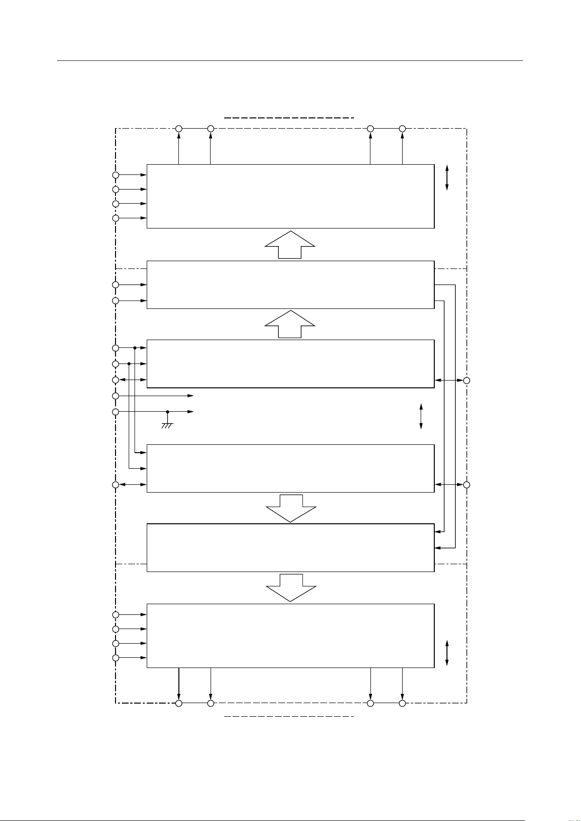
BLOCK DIAGRAM
MSM6568A¡ Semiconductor
V
1R
V
2R
V
5R
V
EER
DF
DISPOFF
SHL
CP
IO
1
V
DDR/L
V
SSR/L
O
O
1
2
80-BIT 4-LEVEL DRIVER
O
79
O
80
V
DD
V
EE
80-BIT LEVEL SHIFTER
80-BIT SHIFT REGISTER
IO
80
V
DD
IO
V
V
V
V
81
1L
2L
5L
EEL
V
SS
80-BIT SHIFT REGISTER
IO
160
80-BIT LEVEL SHIFTER
V
80-BIT 4-LEVEL DRIVER
O
81
O
82
O
159
O
160
DD
V
EE
(V
stands for V
DDR/L
DDR
and V
DDL
, and V
SSR/L
for V
SSR
and V
SSL
.)
2/8
Page 3
PIN CONFIGURATION (TOP VIEW)
MSM6568A¡ Semiconductor
O
160
O
1
Chip Surface
1 2 3 18 19 22
(LCD input side)
Pin Symbol Pin Symbol
(LCD output side)
1V
1L
2V2L13 IO
3V5L14 IO
4V
EEL
5NC16V
6V
DDL
12 IO
15 IO
17 V
160
81
80
1
SSR
DDR
7 SHL 18 NC
8V
SSL
9 DISPOFF 20 V
10 CP 21 V
11 DF 22 V
19 V
EER
5R
2R
1R
NC : No connection
3/8
Page 4

ABSOLUTE MAXIMUM RATINGS
Parameter Symbol Condition Rating Unit
Power Supply Voltage V
Bias Voltage V
Input Voltage V
Storage Temperature T
DD
LCD
I
STG
Ta=25°C –0.3 to +6.5 V
Ta=25°C, V
DD
– V
EE
0 to 30 V
Ta=25°C –0.3 to VDD+0.3 V
— –30 to +85 °C
MSM6568A¡ Semiconductor
*V1>V2>V5>V
EE
VEE<V5£VEE+10V
V
≥V1>V2≥V
DD
VDD=V
DDR=VDDL
V5=V5R=V5L, VEE=V
–10V
DD
, V1=V1R=V1L, V2=V2R=V2L,
EER=VEEL
RECOMMENDED OPERATING CONDITIONS
Parameter Symbol Condition Range Unit
Power Supply Voltage V
Bias Voltage
Operating Temperature T
*V1>V2>V5>V
EE
VEE<V5£VEE+7V
V
≥V1>V2≥V
DD
VDD=V
DDR=VDDL
V5=V5R=V5L, VEE=V
–7V
DD
, V1=V1R=V1L, V2=V2R=V2L,
EER=VEEL
DD
V
LCD
op
V
DD
— 2.7 to 5.5 V
– V
EE
— –20 to +75 °C
No load
LCD being
driven
14 to 28 V
18 to 28 V
4/8
Page 5

ELECTRICAL CHARACTERISTICS
DC Characteristics
Parameter Symbol Condition Min. Typ. Max. Unit
"H" Input Voltage V
"L" Input Voltage V
"H" Input Current I
"L" Input Current I
"H" Output Voltage V
"L" Output Voltage V
ON Resistance R
Supply Current
Input Capacitance C
*1
IH
*1
IL
V
*1
IH
V
*1
IL
*2
OH
*2
OL
*4
ON
I
SS
I
EE
I
MSM6568A¡ Semiconductor
(V
=2.7 to 5.5V, Ta=–20 to +75°C)
DD
— 0.8V
— — — 0.2V
, VDD=5.5V — — 1 mA
I=VDD
=0V, VDD=5.5V — — –1 mA
I
IO=–0.2mA, VDD=2.7V VDD–0.4 — — V
IO=0.2mA, VDD=2.7V — — 0.4 V
V
| V
DD–VEE
|=0.25V
N–VO
=25V
——
*3
——
CP=22kHz, VDD=3.0V — — 50
VDD–VEE=25V, no load*5 — — 300
f=1MHz — 5 — pF
—— V
DD
2.0 kW
DD
V
mA
*1 Applied to CP, IO1, IO80, IO81, IO
*2 Applied to IO1, IO80, IO81, IO
160
, SHL, DF, DISPOFF
160
*3 VN=VDD to VEE, V2=1/16 (VDD – VEE), V5=15/16 (VDD – VEE)
VDD=V1, VDD=4.5V, V1=V1L=V1R, V2=V2L=V2R, V5=V5L=V5R, VEE=V
VDD=V
*4 Applied to O1 to O
DDL=VDDR
160
EEL=VEER,
*5 Input a "H" level signal through the IO pins every 240 clock pulses when a supply current is
measured.
The DF frequency is 45Hz.
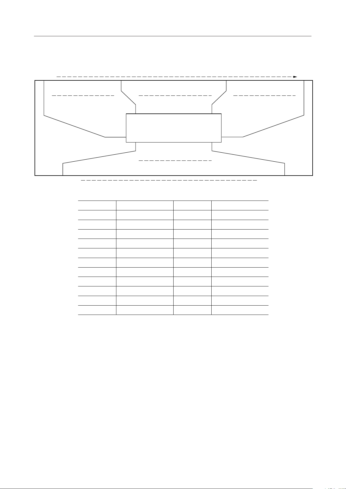
Switching Characteristics
Parameter Symbol Condition Min. Typ. Max. Unit
"H", "L" Propagation Delay Time
Maximum Clock Frequency f
Clock Pulse Width t
Data Setup Time
ÆCP
IO
n
Data Hold Time
CPÆIO
n
Rise Time / Fall Time of CP
*1
*1
t
PHL
t
PLH
WCP
t
setup
t
hold
t
r(CP)
t
f(CP)
CP
———3ms
— 1 — — MHz
— 63——ns
— 100 — — ns
— 100 — — ns
— ——20ns
(V
=2.7 to 5.5V, Ta=–20 to +75°C, CL=15pF)
DD
*1 IOn=IO1-IO
160
5/8
Page 6

MSM6568A¡ Semiconductor
CP
IO
IO
IO
IO
(IO80)
1
(IO
81
(IO1)
80
(IO81)
160
160
t
f(CP)
t
WCP
0.8V
DD
0.2V
DD
t
setup
0.8V
DD
)
0.2V
DD
t
hold
0.8V
0.2V
t
r(CP)
DD
DD
t
PLH(tPHL
0.8V
0.2V
0.8V
DD
DD
DD
)
6/8
Page 7

FUNCTIONAL DESCRIPTION
Pin Functional Description
MSM6568A¡ Semiconductor
•IO1, IO80, IO81, IO
160
Data input/output pins for the two 80-bit bidirectional shift registers.
• SHL
Input pin to select the shift direction of the two 80-bit bidirectional registers.
Table 1 shows the relations between the SHL pin and the IO1, IO80, IO81, IO
160
pins.
•CP
Clock pulse input pin for the two 80-bit bidirectional shift registers.
Scan data shifts at the falling edge of a clock pulse.
•DF
Signal input pin to synchronize with AC current for LCD driving waveforms.
Normally an inverted frame signal is input to this pin.
•V
DDL
, V
DDR
, V
SSL
, V
SSR
Power supply pins.
Normal operating conditions are V
DDR=VDDL
=2.7 to 5.5V, V
SSR=VSSL
=0V.
• DISPOFF
Input pin to control the O1 to O
O1 to O
160
.
•V1L, V1R, V2L, V2R, V5L, V5R, V
outputs. During input of "L" level, V1 levels are output from
160
, V
EEL
EER
Bias voltage input pins for LCD driving. Voltages must be input to all these pins.
•O1 to O
160
4-level driver output pins corresponding to each bit of the shift registers.
The V1, V2, V5, or VEE level is selected and output based on the combination of shift register data
and a DF signal.
Table 2 shows the relations between the scan data and the LCD driving outputs.
SHL Shift direction IO1, IO81 / IO80, IO
, IO
IO
1
IO
80
80
1
, IO
, IO
, IO
81
160
160
81
O
L
1ÆO80
O81ÆO
160
IO
IO
H
O
O80ÆO
1
160ÆO81
Scan data LCD driving output
H Select levels (V
L Non-select levels (V
Table 1
I/O Input
160
and IO81 are data input pins for the shift register.
IO
Input
1
Data is input to these pins in synchronization with clocks
and is output from IO80 and IO
Output
Input
(80) of shift register bits in synchronization with clocks.
IO
and IO
80
are data input pins for the shift register.
160
Data is input to these pins in synchronization with clocks
and is output from IO1 and IO81 with delay by the number
Output
(80) of shift register bits in synchronization with clocks.
Table 2
, VEE)
1
, V5)
2
with delay by the number
160
7/8
Page 8

Truth Table
MSM6568A¡ Semiconductor
DF Shift register data DISPOFF Driver output level (O1-O
LL H V
LH H V
HL H V
HH H V
XX L V
X : Don't Care
EE
)
160
2
5
1
1
8/8
 Loading...