

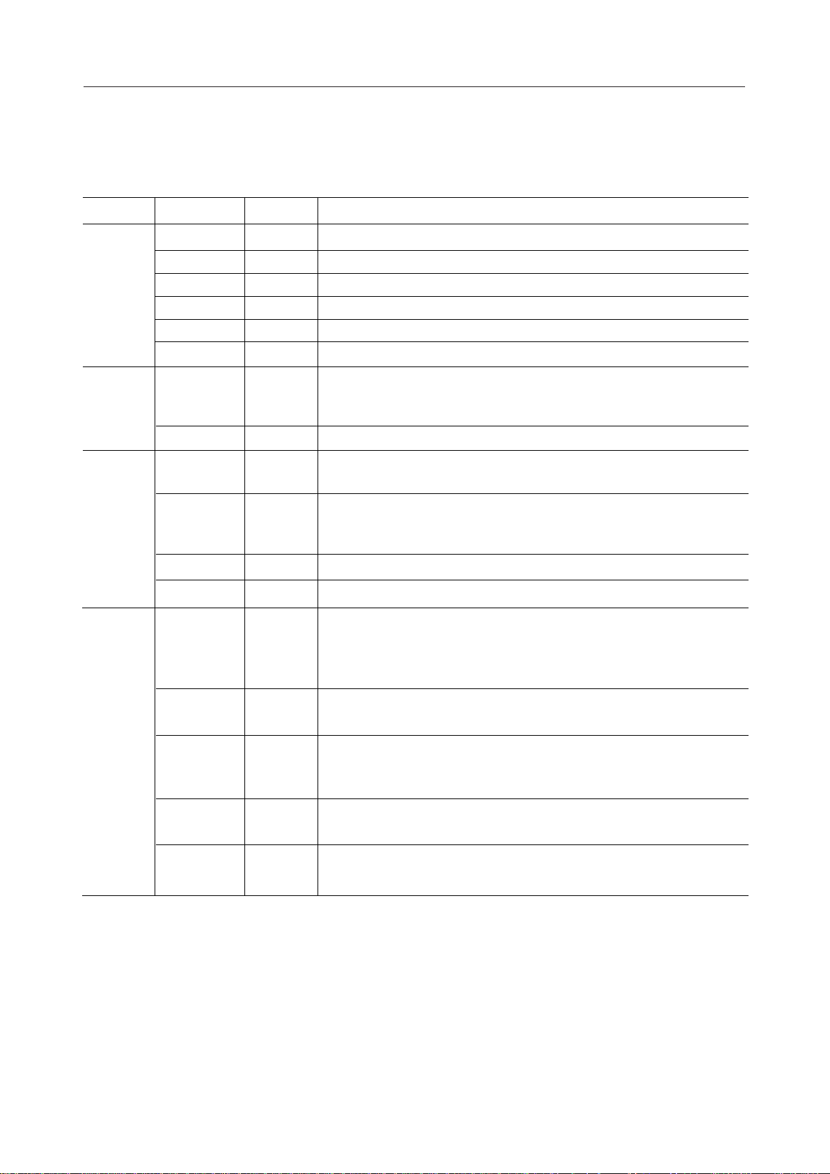
Datasheet MSM65P524-xxxGS-BK, MSM65P524-xxxJS, MSM65P524-xxxSS, MSM65524A-xxxSS, MSM65524A-xxxGS-BK Datasheet (OKI)
...Page 1

E2E1016-27-Y6
¡ Semiconductor MSM65524A/65P524
¡ Semiconductor
This version: Jan. 1998
Previous version: Nov. 1996
MSM65524A/65P524
8-Bit Microcontroller with A/D Converter
GENERAL DESCRIPTION
The MSM65524A is a high-performance 8-bit microcontroller that employs OKI original nX-8/
50 CPU core. With a minimum instruction execution time of 400 ns (10MHz clock), the
MSM65524A is capable of high-speed processing, and includes 16K bytes of program memory,
384 bytes of data memory, timers, serial ports, an A/D converter and PWMs on chip. Also
available are the MSM65P524, which replaces the on-chip program memory with one-time
PROM, and the MSM65X524A, which uses the external program memory.
FEATURES
• Operating range
Operating frequency : 0 to 10MHz (VDD=4.5 to 5.5V)
0 to 5MHz (VDD=2.7 to 5.5V)
Operating voltage : 2.7 to 5.5V
Operating temperature : –40 to +85°C
• Memory space : 64K bytes
Internal program memory : 16K bytes
Internal data memory : 384 bytes
• Minimum instruction execution time : 400ns @ 10 MHz
• Powerful instruction set : 83 basic instructions
8/16-bit operation instructions
Bit manipulation instructions
Compound function instructions
• Abundant addressing modes
• Multiplication/division operation functions : 8 ¥ 8 Æ 16
16 ÷ 8 Æ 16 ... 8
• I/O port
Input-output port : 5 ports ¥ 8 bits
1 port ¥ 4 bits
Input port : 1 port ¥ 8 bits
• Timers : 8-bit auto-reload timer ¥ 2
16-bit auto-reload timer ¥ 1
Watchdog timer ¥ 1
• Counters : Time base counter ¥ 1
16-bit free-running counter ¥ 1
• Capture input : 1 channel
• Compare output : 2 channels
• Serial ports : Shift register ¥ 1
Serial port with baud rate generator
(UART/Synchronous) ¥ 1
• A/D converter : 8 bits ¥ 8 channels
• PWM : 8 bits ¥ 2 channels
PWM with auto-reload timer for period
setting
1/27
Page 2

¡ Semiconductor MSM65524A/65P524
• External interrupts : 3
• Interrupt sources : 19
• Package options
64-pin plastic shrink DIP (SDIP64-P-750-1.78) : (Product name: MSM65524A-¥¥¥SS,
MSM65P524-¥¥¥SS)
64-pin plastic QFP (QFP64-P-1414-0.80-BK) : (Product name: MSM65524A-¥¥¥GS-BK,
MSM65P524-¥¥¥GS-BK)
68-pin plastic QFJ (PLCC) (QFJ68-P-S950-1.27): (Product name: MSM65524A-¥¥¥JS,
MSM65P524-¥¥¥JS)
¥¥¥ indicates the code number.
2/27
Page 3
3/27
¡ Semiconductor MSM65524A/65P524
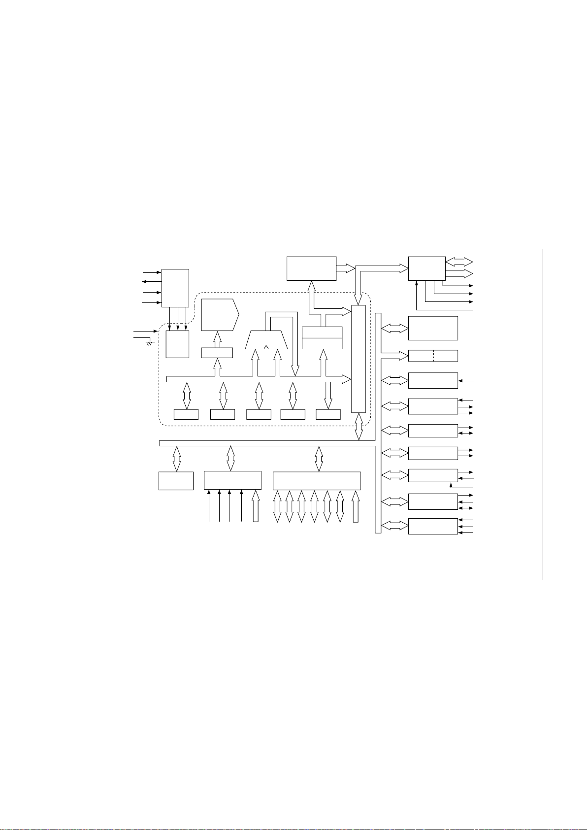
BLOCK DIAGRAM
OSC 0
OSC 1
RESET
HSTOP*
V
DD
GND
OSC
CONT.
ROM
(16K bytes)
EXT.MEM.
CONT.
CPU CORE
INST.
DEC.
T/C
IR
ALU
GMAR
PC
AR BR PSW SP LMAR
BUS
CONT.
I/O PORT
RAM
(384 bytes)
TBC WDT
16-bit TIMER
16-bit FRC
CAP¥1, CMP¥2
SIO
AD0-7*
A8-15*
RD
WR*
ALE
EA
T2CK*
GATE*
CAP*
CMP0*
CMP1*
TXD*
RXD*
P2 P3 P4 P5
* Secondary functions of ports
8
8
8
8
8
8-bit TIMER¥4**
T1OUT*
T0CK*
8-bit SHIFT-REG.
INTERRUPT CONT.
SFTO*
SFTI*
SFTCK*
INT0*
INT1*
INT2*
MUL/DIV
P1P0 P6
8-bit PWM¥2
PWM0*
PWM1*
8-bit A/D C ¥ 8ch
** One timer doubles as the SIO baud rate
generator, another doubles as a PWM
clock source.
AVDDVRHVRLAGND
AI0*- AI7*
Page 4
¡ Semiconductor MSM65524A/65P524
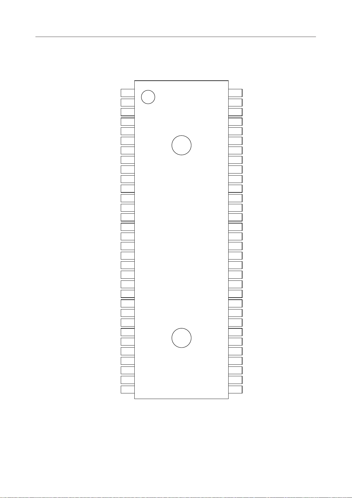
PIN CONFIGURATION (TOP VIEW)
P5.0/PWM0
P5.1/PWM1
P5.2
P5.3
P4.0
P4.1
P4.2
P4.3
P4.4
P4.5
P4.6
P4.7
P3.0/T2CK
P3.1/CAP
P3.2/CMP0
P3.3/CMP1
P3.4/INT2
P3.5/SFTO
P3.6/SFTI
P3.7/SFTCK
RESET P0.7/AD7
P2.0/RXD EA
P2.1/TXD ALE
P2.2/INT0 RD
P2.3/INT1/GATE P1.7/A15
P2.4/T0CK P1.6/A14
P2.5/HSTOP P1.5/A13
P2.6/WR P1.4/A12
P2.7/T1OUT P1.3/A11
OSC1 P1.2/A10
OSC0 P1.1/A9
GND P1.0/A8
1
2
3
4
5
6
7
8
9
10
11
12
13
14
15
16
17
18
19
20
21
22
23
24
25
26
27
28
29
30
31
32
64
63
62
61
60
59
58
57
56
55
54
53
52
51
50
49
48
47
46
45
44
43
42
41
40
39
38
37
36
35
34
33
V
DD
AV
DD
V
RH
V
RL
P6.7/AI7
P6.6/AI6
P6.5/AI5
P6.4/AI4
P6.3/AI3
P6.2/AI2
P6.1/AI1
P6.0/AI0
AGND
P0.0/AD0
P0.1/AD1
P0.2/AD2
P0.3/AD3
P0.4/AD4
P0.5/AD5
P0.6/AD6
64-Pin Plastic Shrink DIP
4/27
Page 5
¡ Semiconductor MSM65524A/65P524
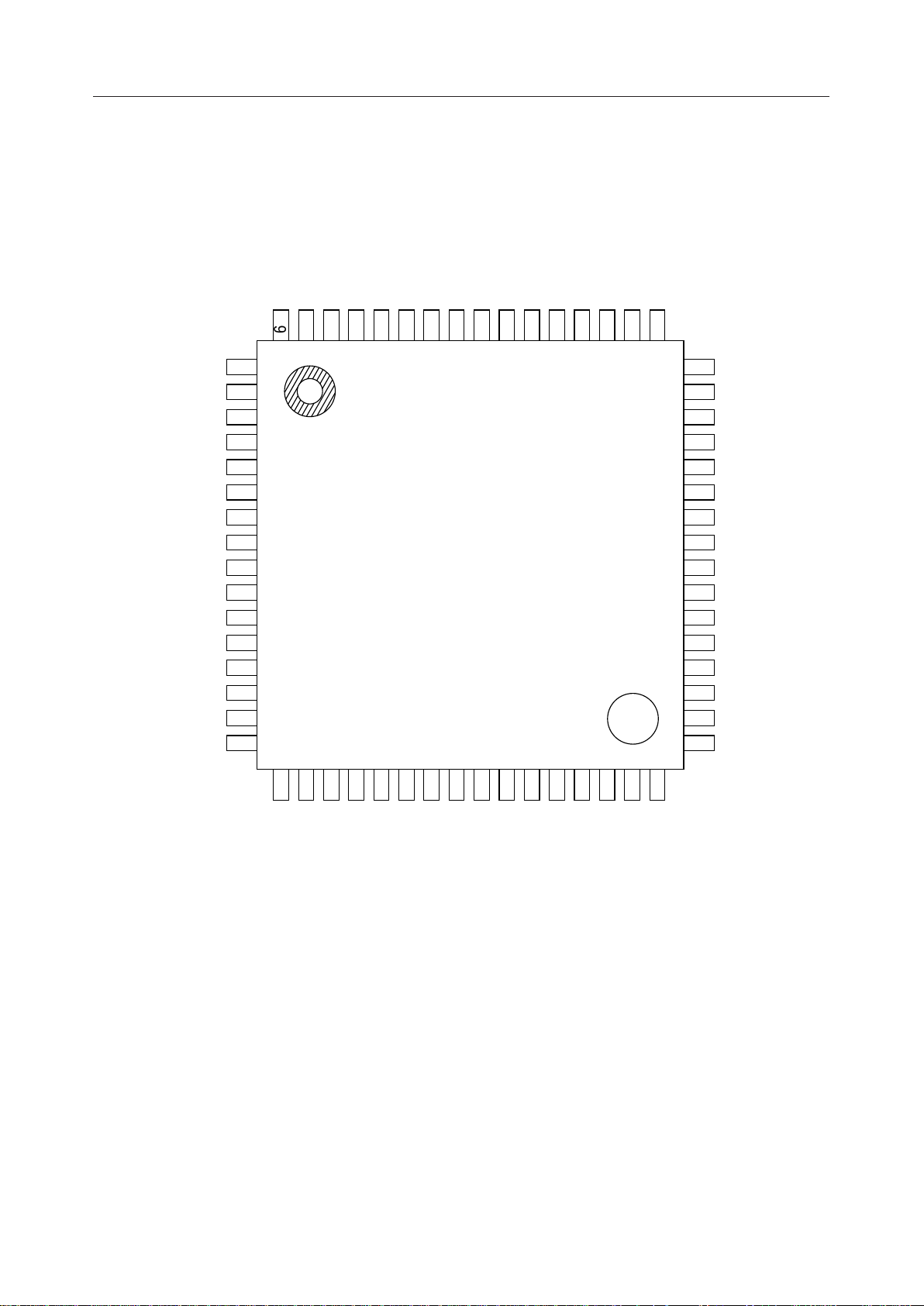
PIN CONFIGURATION (TOP VIEW) (Continued)
P4.4
P4.5
P4.6
P4.7
P3.0/T2CK
P3.1/CAP
P3.2/CMP0
P3.3/CMP1
P3.4/INT2
P3.5/SFTO
P3.6/SFTI
10
11
12P3.7/SFTCK
13RESET
14P2.0/RXD
15P2.1/TXD
16P2.2/INT0
P4.3
P4.2
P4.1
P4.0
P5.3
P5.2
P5.1/PWM1
64
63
62
61
60
59
58
1
2
3
4
5
6
7
8
9
DD
P5.0/PWM0
V
57
56
AVDDV
55
RH
54
53 VRL52 P6.7/AI7
54 P6.6/AI6
50 P6.5/AI5
49 P6.4/AI4
48
47
46
45
44
43
42
41
40
39
38
37 P0.6/AD6
36 P0.7/AD7
35 EA
34 ALE
33 RD
P6.3/AI3
P6.2/AI2
P6.1/AI1
P6.0/AI0
AGND
P0.0/AD0
P0.1/AD1
P0.2/AD2
P0.3/AD3
P0.4/AD4
P0.5/AD5
17
18
19
20
P2.4/T0CK
P2.3/INT1/GATE
P2.6/WR
P2.5/HSTOP
21
22
23
24
25
26
OSC0
GND
P1.0/A8
P1.1/A9
OSC1
P2.7/T1OUT
64-Pin Plastic QFP
27
28P1.3/A11
P1.2/A10
29P1.4/A12
30P1.5/A13
31P1.6/A14
32P1.7/A15
5/27
Page 6
¡ Semiconductor MSM65524A/65P524
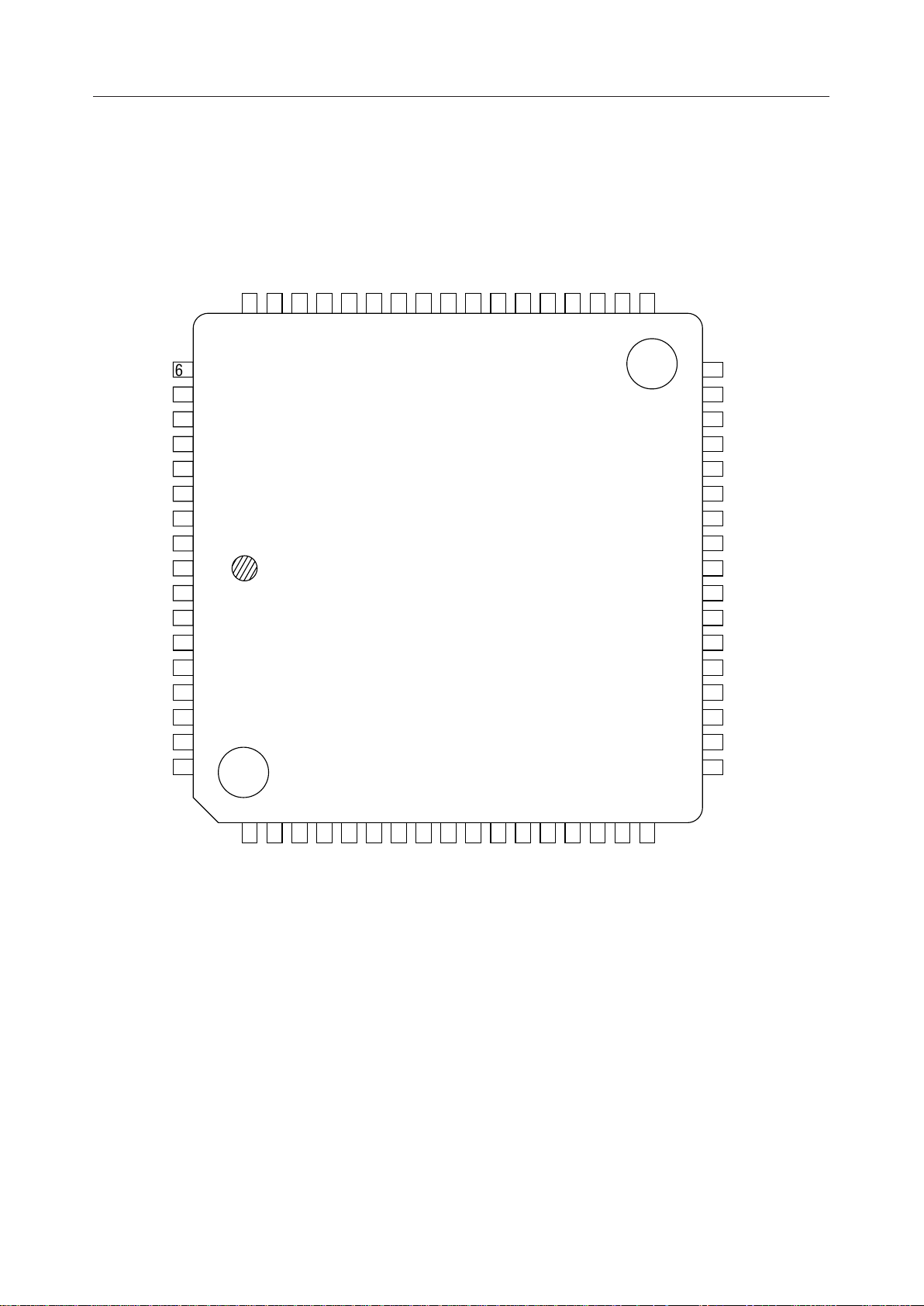
PIN CONFIGURATION (TOP VIEW) (Continued)
P6.3/AI3
P6.2/AI2
P6.1/AI1
P6.0/AI0
AGND
P0.0/AD0
P0.1/AD1
60
59
58
57
56
55
P0.2/AD2
54
53
P0.3/AD3
52
P0.4/AD4
51
P0.5/AD5
50
P0.6/AD6
49
P0.7/AD7EAALE
48
47
46
45
RD
44
P6.4/AI4
P6.5/AI5
P6.6/AI6
P6.7/AI7
V
RL
V
RH
AV
DD
NC
V
DD
P5.0/PWM0
P5.1/PWM1
P5.2
P5.3
P4.0
P4.1
P4.2
P4.3
61
62
63
64
65
66
67
68
P1.7/A15
43
P1.6/A14
42
P1.5/A13
41
P1.4/A12
40
P1.3/A11
39
P1.2/A10
38
P1.1/A9
37
P1.0/A8
36
1
2
3
4
5
6
7
8
9
NC
35
GND
34
OSC0
33
OSC1
32
P2.7/T1OUT
31
P2.6/WR
30
P2.5/HSTOP
29
P2.4/T0CK
28
P2.3/INT1/GATE
27
10
P4.4
11
P4.5
12
13
14
15
16
17
18
P4.6
P4.7
P3.0/T2CK
P3.1/CAP
P3.2/CMP0
NC NC
P3.3/CMP1
NC: No-connection pin
68-Pin Plastic QFJ (PLCC)
19
20
P3.4/INT2
P3.6/SFTI
P3.5/SFTO
21
22
P3.7/SFTCK
23
24
RESET
P2.0/RXD
25
26
P2.1/TXD
P2.2/INT0
6/27
Page 7
¡ Semiconductor MSM65524A/65P524
PIN DESCRIPTION
Basic Functions
Function Symbol Type Description
Power
Supply
Oscillation
Control
V
DD
GND
AV
DD
AGND
V
RH
V
RL
OSC0
—
—
—
—
—
—
I
+5V digital power supply
0V digital ground
+5V analog power supply
0V analog ground
+5V analog reference voltage
0V analog reference voltage
System clock input pin. Quartz oscillator or ceramic oscillator is
connected between OSC0 and OSC1. For external clock, input at OSC0,
leaving OSC1 open.
OSC1
RESET System reset input (program starts from address 0040H);
O
I
System clock output pin
internal pull-up resistance
EA Program memory select input pin.
I
"L" level input for external program memory; "H" level input for internal
program memory.
RD Read strobe signal during external memory accessO
ALE Address latch signal during external memory accessO
PORT 0 8-bit Input-output port
I/O
During external memory access, becomes address/data bus for address
output, instruction fetch or data read/write along with ALE, RD and WR
pins.
Port
PORT 1 8-bit Input-output port
I/O
Address bus during external memory access
PORT 2
PORT 3
I/O
8-bit Input-output port ¥ 3. Secondary functions shown in following table
are added for ports 2 and 3.
PORT 4
PORT 5 4-bit Input-output port
I/O
Secondary functions shown in following table are added for port 5.
PORT 6 8-bit Input port
I
Functions as analog input channel during A/D conversion.
7/27
Page 8

¡ Semiconductor MSM65524A/65P524
Secondary Functions
Symbol Type Description
RXD P2.0 secondary function
TXD P2.1 secondary function
INT0 P2.2 secondary function
INT1/GATE P2.3 secondary functions
T0CK P2.4 secondary function
HSTOP P2.5 secondary function
WR P2.6 secondary function
T1OUT P2.7 secondary function
I/O
UART: Input pin for serial port receive data.
Synchronous: Input/output pin for serial port transmit/receive data.
O
UART: Output pin for serial port transmit data.
Synchronous: Output pin for serial port synchronizing clock.
I
External interrupt 0 input pin.
I
External interrupt 1 input pin. Also used as input pin for gate signal
for timer 0 count enable/disable.
I
Timer 0 external clock input pin.
I
Hard stop mode input pin; stops system clock oscillation with "L" level input.
O
Write strobe signal output pin during external data memory access.
O
Output pin for signal that 2-divided timer 1 overflow.
T2CK P3.0 secondary function
CAP P3.1 secondary function
CMP0 P3.2 secondary function
CMP1 P3.3 secondary function
INT2 P3.4 secondary function
SFTO P3.5 secondary function
SFTI P3.6 secondary function
SFTCK P3.7 secondary function
PWM0 P5.0 secondary function
I
Timer 2 external clock input pin.
I
Capture trigger input pin.
O
Compare output channel 0 output pin.
O
Compare output channel 1 output pin.
I
External interrupt 2 input signal.
O
Shift register data output pin.
I
Shift register data input pin.
I/O
Shift register synchronizing clock input/output pin.
O
PWM channel 0 output pin.
PWM1 P5.1 secondary function
O
PWM channel 1 output pin.
8/27
Page 9
¡ Semiconductor MSM65524A/65P524
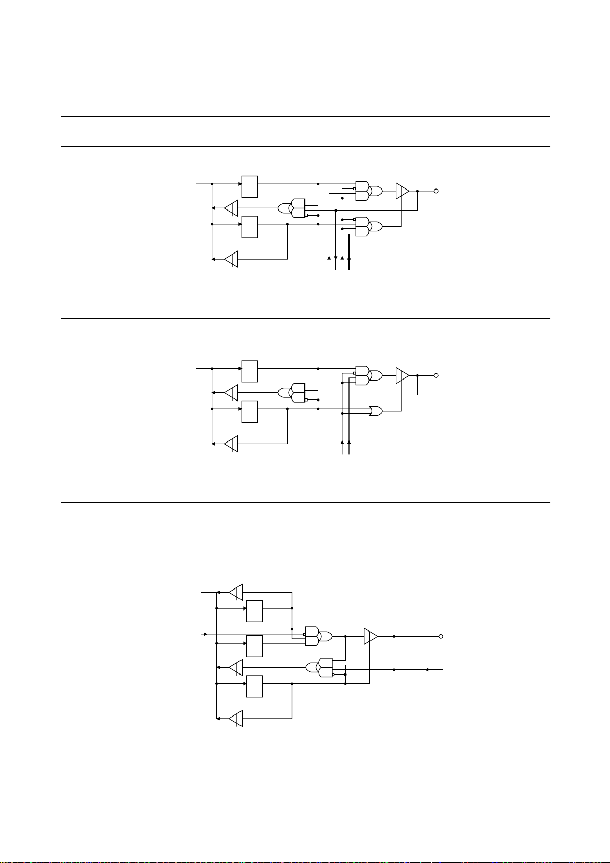
Port Circuit Configuration
Type Port
P0.0/AD0 to
1
P0.7/AD7
P1.0/A8 to
2
P1.7/A15
Data Bus
Data Bus
Circuit Configuration
P0D
P0
DIR
External Memory Control
P1D
P1
DIR
PORT0
PORT1
Electrical Characteristics
(V
=5V)
DD
"H" Input Voltage:
• V
=2.4V
IH
"L" Input Voltage:
• V
=0.8V
IL
"H" Output Voltage:
• V
=3.75V
OH
• I
=–400mA
OH
"L" Output Voltage:
• V
=0.4V
OL
• I
=3.2mA
OL
"H" Input Voltage:
• V
=2.4V
IH
"L" Input Voltage:
• V
=0.8V
IL
"H" Output Voltage:
• V
=3.75V
OH
• I
=–200mA
OH
3
P2.0/RXD,
P2.1/TXD,
P2.6/WR,
P2.7/T1OUT,
P3.2/CMP0,
P3.3/CMP1,
P3.5/SFTO,
P3.7/SFTCK,
P5.0/PWM0,
P5.1/PMW1
Data Bus
Secondary
Output
Function
Px
MOD
PxD
Px
DIR
External Memory Control
PORTx
Secondary
Input
Function
(x=2 to 5)
"L" Output Voltage:
• V
=0.4V
OL
• I
=1.6mA
OL
"H" Input Voltage:
• V
=2.4V
IH
"L" Input Voltage:
• V
=0.8V
IL
P2.6/WR
"H" Output Voltage:
• V
=3.75V
OH
• I
=–400mA
OH
"L" Output Voltage:
• V
=0.4V
OL
• I
=3.2mA
OL
Ports other than
P2.6/WR
"H" Output Voltage:
• V
=3.75V
OH
• I
=–200mA
OH
"L" Output Voltage:
• V
=0.4V
OL
• I
=1.6mA
OL
9/27
Page 10

¡ Semiconductor MSM65524A/65P524
Port Circuit Configuration (Continued)
Type Port
P2.2/INT0,
P2.3/INT1/GATE,
P2.4/T0CK,
P2.5/HSTOP,
P3.0/T2CK,
4
P3.1/CAP,
P3.4/INT2,
P3.6/SFTI,
P4.0 to P4.7,
P5.2 to P5.3
P6.0/AI0 to
5
P6.7/AI7
Data Bus
Data Bus
Circuit Configuration
PxD
Px
DIR
PORTx
Secondary
Input Function
(x=2 to 5)
PORT6
To A/D Converter
Electrical Characteristics
(V
=5V)
DD
"H" Input Voltage:
• V
=2.4V
IH
"L" Input Voltage:
• V
=0.8V
IL
"H" Output Voltage:
• V
=3.75V
OH
• I
=–200mA
OH
"L" Output Voltage:
• V
=0.4V
OL
• I
=1.6mA
OL
"H" Input Voltage:
• V
=2.4V
IH
"L" Input Voltage:
• V
=0.8V
IL
10/27
Page 11

¡ Semiconductor MSM65524A/65P524
MEMORY MAPS
General Memory Space
0FFFFH
External Memory
Local Memory Space
1FFH
Data Memory
Page 1
4000H
100H
80H
40H
30H
20H
10H
Data Memory
Local Register Set 3
Local Register Set 2
Local Register Set 1
Local Register Set 0
0
SFR
Page 0
Program Memory
100H
Vector Call Table Area
80H
40H
20H
Program Memory
Interrupt Vector Table Area
Vector Call Table Area
0
Internal Memory
11/27
Page 12

¡ Semiconductor MSM65524A/65P524
2
5
4
6
8
10
23456
1
5.5
Ta=–40 to +85°C
f
OSC
, f
EXTCLK
(MHz)
Oscillator
Frequency > 1MHz
V
DD
(V)
2.7
ABSOLUTE MAXIMUM RATINGS
Parameter Unit
Supply Voltage VDD=AV
Input Voltage V
Output Voltage V
Analog Reference Voltage
Analog Input Voltage
Power Dissipation
Storage Temperature T
Symbol Condition Rating
DD
O
VRH, V
V
AI
P
D
STG
I
RL
Ta=25°C
GND=AGND=0V
RECOMMENDED OPERATING CONDITIONS
Parameter Unit
Supply Voltage V
Analog Supply Voltage AV
Analog Reference Voltage V
Analog Input Voltage V
Memory Hold Voltage V
Operating Frequency *
1
Symbol Condition Range
DD
DD
RH
AI
DDMH
f
OSC
Refer to Figure 1.
VDD=AVDD=V
GND=AGND=VRL=0V
=0 Hz
OSC
RH
–0.3 to 7.0
–0.3 to VDD+0.3
–0.3 to VDD+0.3
–0.3 to VDD+0.3
–0.3 to V
DD
+0.3
400Ta=25°C per package
–55 to +150—
2.7 to 5.5
2.7 to 5.5
2.7 to 5.5
0 to V
DD
2.0 to 5.5f
1 to 10Refer to Figure 1.
V
mW
°C
V
MHz
External Clock Operating
f
Frequency
Operating Temperature T
EXTCLK
op
*1 This is due to the standard of a crystal oscillator or resonator.
Figure 1. Power Supply Voltage vs. Operating Frequency
0 to 10Refer to Figure 1.
–40 to +85—
MHz
°C
12/27
Page 13

¡ Semiconductor MSM65524A/65P524
ELECTRICAL CHARACTERISTICS
DC Characteristics 1 (VDD=4.5 to 5.5V)
(GND=0V, Ta=–40 to +85°C)
Parameter Symbol Condition Min. Typ. Max. Unit
"H" Input Voltage 1 V
"H" Input Voltage 2 V
"L" Input Voltage V
"H" Output Voltage 1 V
"H" Output Voltage 2 V
"L" Output Voltage 1 V
"L" Output Voltage 2 V
Input Leakage Current 1 I
Input Leakage Current 2 I
"L" Input Current I
Input Capacitance C
Static Current Consumption I
*1
*2
*3
*4
*3
*4
*5
*6
*7
IH1
IH2
IL
OH1
OH2
OL1
OL2
LI1
LI2
IL
DDS
—
— 0.7V
2.4
DD
—VDD+0.3
—VDD+0.3
— –0.3 — 0.8
IOH=–200mA 0.75V
IOH=–400mA 0.75V
DD
DD
——
——
V
IOL=1.6mA — — 0.4
IOL=3.2mA — — 0.4
VI=VDD/0V — — ±1
VI=VDD/0V — — ±10
VI=0V
I
f=1MHz, Ta=25°C — 5 —
5V, stop mode
*8
–40 –120 –400
——50
mA
pF
mA
10MHz, 5V, no load
Dynamic Current Consumption I
DD
Refer to Figure2
—2040
*1 Excluding OSC0 and RESET
*2 OSC0 and RESET
*3 Excluding P0, ALE, RD, P2.6/WR
*4 P0, ALE, RD, P2.6/WR
*5 EA, P6
*6 Excluding RESET, EA, P6
*7 RESET
*8 The ports set for input mode are VDD or 0V and the ports except these are no load.
mA
13/27
Page 14

¡ Semiconductor MSM65524A/65P524
DC Characteristics 2 (2.7
££
£VDD<4.5V)
££
Parameter Symbol Condition Min. Typ. Max. Unit
"H" Input Voltage 1 V
"H" Input Voltage 2 V
*1
*2
"L" Input Voltage V
"H" Output Voltage 1 V
"H" Output Voltage 2 V
"L" Output Voltage 1 V
"L" Output Voltage 2 V
Input Leakage Current 1 I
Input Leakage Current 2 I
"L" Input Current I
*3
*4
*3
*4
*5
*6
*7
Input Capacitance C
Static Current Consumption I
Dynamic Current Consumption I
IH1
IH2
IL
OH1
OH2
OL1
OL2
LI1
LI2
IL
DDS
DD
(GND=0V, Ta=–40 to +85°C)
—
—
— –0.3 —
IOH=–10mA 0.75V
IOH=–20mA 0.75V
0.5VDD+0.2
0.6VDD+0.4
DD
DD
—VDD+0.3
—VDD+0.3
0.15VDD+0.1
——
——
V
IOL=10mA — — 0.1
IOL=20mA — — 0.1
VI=VDD/0V — — ±1
VI=VDD/0V — — ±10
mA
VDD=2.7 to 3.3V
–40 –120 –240
VI=0V
I
f=1MHz, Ta=25°C — 5 —
3V, stop mode
*8
——25
pF
mA
5MHz, 3V, no load
Refer to Figure 2
—615
mA
*1 Excluding OSC0 and RESET
*2 OSC0 and RESET
*3 Excluding P0, ALE, RD, P2.6/WR
*4 P0, ALE, RD, P2.6/WR
*5 EA, P6
*6 Excluding RESET, EA, P6
*7 RESET
*8 The ports set for input mode are VDD or 0V and the ports except these are no load.
14/27
Page 15

10
20
30
40
50
23456
I
DD
(mA)
VDD (V)
10
20
30
40
50
23456
I
DD
(mA)
VDD (V)
10
20
30
40
50
23456
I
DD
(mA)
VDD (V)
10MHz
Max.
Typ.
Max.
Typ.
Max.
Typ.
6MHz
2MHz
Ta=–40 to +85°C, no load
¡ Semiconductor MSM65524A/65P524
Figure 2. Voltage vs. Current
15/27
Page 16

¡ Semiconductor MSM65524A/65P524
AC Characteristics
• External memory control
(VDD=AVDD=VRH=2.7 to 5.5V, GND=AGND=VRL=0V, Ta=–40 to +85°C)
Parameter Symbol Condition Min. Max. Unit
Clock Period t
"L" Clock Pulse Width t
"H" Clock Pulse Width t
Clock Period t
"L" Clock Pulse Width t
"H" Clock Pulse Width t
ALE Pulse Width t
ALE Pulse Delay Time 1 t
ALE Pulse Delay Time 2 t
RD Pulse Width t
RD Pulse Delay Time t
WR Pulse Width t
WR Pulse Delay Time t
"L" Address Setup Time t
"H" Address Setup Time t
"L" Address Hold Time t
C
CLW
CHW
C
CLW
CHW
AW
ALD1
ALD2
RW
RD
WW
WD
LAS
HAS
LAH
VDD=4.5 to 5.5V
VDD=2.7 to 5.5V
CL=100pF
100 —
45 —
45 —
200 —
90 —
90 —
tC+t
tC+t
tC+t
–20 —
CHW
t
–20 —
CLW
t
–20 —
CLW
–20 —
CHW
t
–20 t
CLW
–40 —
CHW
t
–20 t
CLW
tC–40 —
tC–40 —
t
–20 —
CLW
CLW
CLW
+20
ns
+40
Bus Float Time t
"H" Address Hold Time t
"H" Address Hold Time t
Read Data Access Time t
Read Data Access Time t
Read Data Hold Time t
Write Data Setup Time t
Write Data Hold Time t
LAZ
HAHR
HAHW
RDAA
RDAR
RDH
WDS
WDH
—20
tC–20 —
tC–20 —
—t
—t
C+tCLW
CHW
–15
+10
0—
tC+t
–40 —
CHW
t
–20 —
CLW
16/27
Page 17

¡ Semiconductor MSM65524A/65P524
OSC0
ALE
RD
P0
P1
t
CHW
t
CLW
t
C
t
AW
t
LAS
ADDRESS L
t
HAS
t
t
LAH
t
RD
t
RDAA
RDAR
t
LAZ
t
RW
INST or
DATA IN
t
ALD1
t
RDH
t
HAHR
ADDRESS H
WR
P0
P1
t
WD
t
WW
t
WDS
ADDRESS L DATA OUT
ADDRESS H
t
ALD2
t
WDH
t
HAHW
17/27
Page 18

¡ Semiconductor MSM65524A/65P524
• CPU control
(VDD=AVDD=VRH=2.7 to 5.5V, GND=AGND=VRL=0V, Ta=–40 to +85°C)
Parameter Symbol Condition Min. Max. Unit
RESET Pulse Width
RESET Pulse Width
*1
*2
t
RESW1
t
RESW2
—
—
20 — ns
*3
—
—
*1 Excluding power ON, stop mode and hard stop mode.
*2 In power ON, stop mode and hard stop mode.
*3 Oscillation stabilization time depends on resonator.
RESET Pulse Width
t
RESW1, 2
RESET
• Peripheral control 1
Parameter Symbol Condition Min. Max. Unit
OSC
EXI
T0
T2
*1 t
Clock Period t
External Interrupt Pulse
Width
External Clock Pulse
Width
GATE Pulse Width t
External Clock Pulse
Width
CAP Pulse Width t
: Timer 0 count clock period selected by T0CON.
T0CLK
(VDD=AVDD=VRH=2.7 to 5.5V, GND=AGND=VRL=0V, Ta=–40 to +85°C)
t
EXIW
t
T0CW
C
=2.7 to 5.5V
V
DD
VDD=4.5 to 5.5V
100 —
200 —
4 t
4 t
C
C
—
—
—
T0GW
t
T2CW
CAPW
1 t
TOCLK
4 t
C
12 t
*1
—
—
C
—CAP
ns
18/27
Page 19

¡ Semiconductor MSM65524A/65P524
t
C
OSC0
t
CLW
1) EXI pulse width
t
EXIW
INT0-2
2) T0
T0CK
GATE
3) T2
T2CK
4) CAP
t
T0CW
t
T0GW
t
T2CW
t
CAPW
CAP
19/27
Page 20

¡ Semiconductor MSM65524A/65P524
• Peripheral control 2
(VDD=AVDD=VRH=2.7~5.5V, GND=AGND=VRL=0V, Ta=–40 to +85°C)
Parameter Symbol Condition Min. Max. Unit
OSC
SFT
SIO
(Clock
Synchro-
nous
Mode)
Clock Period t
SFTCK Period t
SFTCK "L" Pulse Width t
SFTCK "H" Pulse Width t
SFCLW
SFCHW
SFTCK Setup Time t
SFTO Hold Time t
SFTI Setup Time t
SFTI Hold Time t
Synchronous Clock Period
Synchronous Clock "L"
t
Pulse Width
Synchronous Clock "H"
t
SICHW
Pulse Width
Output Data Setup Time t
Output Data Hold Time t
Input Data Setup Time t
C
SFC
SFOS
SFOH
SFIS
SFIH
t
SIC
SICLW
SIOS
SIOH
SIIS
V
=4.5 to 5.5V
DD
=2.7 to 5.5V
DD
CL=100pF
100 —
200 —V
8 t
C
4 tC–20 —
4 tC–20 —
t
–100 —
SFCLW
t
–100 —
SFCHW
100 —
100 —
8 t
C
4 tC–20 —
4 tC–20
6 tC–100 —
2 tC–100 —
tC+t
+100 —
CLW
—
ns
—
—
Input Data Hold Time t
SIIH
0—
20/27
Page 21

¡ Semiconductor MSM65524A/65P524
1) SFT
t
SFC
SFTCK
t
SFCLW
t
SFCHW
SFTO
SFTI
2) SIO
TXD
(Clock synchronous mode)
t
SFOS
t
SFIS
t
SICLW
t
SIC
t
SFOH
t
SFIH
t
SICHW
RXD (transmission)
RXD (reception)
t
SIOS
t
SIIS
t
SIOH
t
SIIH
21/27
Page 22

¡ Semiconductor MSM65524A/65P524
A/D Converter Characteristics 1
(VDD=AVDD=VRH=5V±10%, GND=AGND=VRL=0V, Ta=-40 to +85°C)
Parameter Symbol Condition Min. Max. Unit
Typ.
Resolution n
See the recommended circuit (Fig. 3).
Absolute Error E
L
Analog input source impedance
R
£5kW
f
OSC
I
=10 MHz
Differential Linearity Error E
Zero Point Error E
Full Scale Error E
Crosstalk E
Conversion time * t
D
ZS
FS
CT
CONV
See the measuring circuit (Fig. 4).
* The transition time after the G0 bit goes to "1" is 14.8ms/CH.
A/D Converter Characteristics 2
(VDD=AVDD=VRH=2.7 to 4.5V, GND=AGND=VRL=0V, Ta=-40 to +85°C)
Parameter Symbol Condition Min. Max. Unit
Resolution n
Absolute Error E
Differential Linearity Error E
L
D
See the recommended circuit (Fig. 3).
Analog input source impedance
R
£5kW
I
—
—
—
—
—
—
—
—
—
8
—
—
—
—
—
Typ.
8
—
—
—
+1.5
–1.5
±0.5
+1.5
–1.5
±0.5
—16—
—
+2
–2
±1
bit
LSB
LSB
LSB
LSB
LSB
ms/CH
bit
LSB
LSB
Zero Point Error E
Full Scale Error E
Crosstalk E
Conversion time * t
ZS
FS
CT
CONV
See the measuring circuit (Fig. 4).
=5 MHz
f
OSC
* The transition time after the G0 bit goes to "1" is 29.6ms/CH.
—
—
—
—
—
—
+2
–2
±1
—32—
LSB
LSB
LSB
ms/CH
22/27
Page 23

¡ Semiconductor MSM65524A/65P524
• Definitions of terms
(1) Resolution
The minimum distinguishable analog value. For 8 bits, 28=256, i.e. (VRH–V
) ÷ 256.
RL
(2) Linearity Error
The variance between the ideal conversion characteristics as an 8-bit A/D converter and
actual conversion characteristics (does not include quantatized error).
The ideal conversion characteristics refer to steps of the voltage between VRH and V
into 256 intervals.
(3) Differential Linearity Error
Indicates the smoothness of the conversion. The width of analog input voltage
corresponding to the change by one bit of digital output is 1 LSB = (VRH-V
ideally. The variance between this ideal bit size and bit size at arbitrary point in the
conversion range.
(4) Zero Scale Error
The variance between the ideal conversion characteristics at the switching point of digital
output "000H to 001H" and actual conversion characteristics.
(5) Full Scale Error
The variance between the ideal conversion characteristics at the switching point of digital
output "0FEH to 0FFH" and actual conversion characteristics.
) ÷ 256
RL
RL
23/27
Page 24

¡ Semiconductor MSM65524A/65P524
0.1
AV
V
RH
DD
V
DD
mF
+5V
Analog Voltage
Input
MSM65524A
+
0.1
mF
R
–
1
47
mF
AI0-7
+
0V
V
RL
AGND
GND
0.1
mF
(Analog input source impedance)£5kW
R
I
Figure 3. Recommended Circuit
Analog Voltage
Input
–
+
5kW
AI0
AI1
Crosstalk is defined
as the difference of
A/D conversion result
0.1
mF
between supplying
the same voltage to AI0
to AI7 and supplying
voltage shown in this
diagram.
AI7
V
or AGND
REF
Figure 4. Crosstalk Measuring Circuit
24/27
Page 25

¡ Semiconductor MSM65524A/65P524
PACKAGE DIMENSIONS
(Unit : mm)
SDIP64-P-750-1.78
Package material
Lead frame material
Pin treatment
Solder plate thickness
Package weight (g)
Epoxy resin
Cu alloy
Solder plating
5 mm or more
8.70 TYP.
Notes for Mounting the Surface Mount Type Package
The SOP, QFP, TSOP, SOJ, QFJ (PLCC), SHP and BGA are surface mount type packages, which
are very susceptible to heat in reflow mounting and humidity absorbed in storage.
Therefore, before you perform reflow mounting, contact Oki’s responsible sales person for the
product name, package name, pin number, package code and desired mounting conditions
(reflow method, temperature and times).
25/27
Page 26

¡ Semiconductor MSM65524A/65P524
(Unit : mm)
QFP64-P-1414-0.80-BK
Mirror finish
Package material
Lead frame material
Pin treatment
Solder plate thickness
Package weight (g)
Epoxy resin
42 alloy
Solder plating
5 mm or more
0.87 TYP.
Notes for Mounting the Surface Mount Type Package
The SOP, QFP, TSOP, SOJ, QFJ (PLCC), SHP and BGA are surface mount type packages, which
are very susceptible to heat in reflow mounting and humidity absorbed in storage.
Therefore, before you perform reflow mounting, contact Oki’s responsible sales person for the
product name, package name, pin number, package code and desired mounting conditions
(reflow method, temperature and times).
26/27
Page 27

¡ Semiconductor MSM65524A/65P524
(Unit : mm)
QFJ68-P-S950-1.27
Mirror finish
Package material
Lead frame material
Pin treatment
Solder plate thickness
Package weight (g)
Epoxy resin
Cu alloy
Solder plating
5 mm or more
4.50 TYP.
Notes for Mounting the Surface Mount Type Package
The SOP, QFP, TSOP, SOJ, QFJ (PLCC), SHP and BGA are surface mount type packages, which
are very susceptible to heat in reflow mounting and humidity absorbed in storage.
Therefore, before you perform reflow mounting, contact Oki’s responsible sales person for the
product name, package name, pin number, package code and desired mounting conditions
(reflow method, temperature and times).
27/27
 Loading...