

Page 1
E2B0009-27-Y2
¡ Semiconductor
This version: Nov. 1997
Previous version: Mar. 1996
MSM6544¡ Semiconductor
MSM6544
42-DOT LCD DRIVER
GENERAL DESCRIPTION
The MSM6544 is a 42-segment duplex driver which can drive the LCD panel up to a maximum
of 84 segments.
Since the package is a 56-pin small QFP, an LCD module can be compactly configured. An
internal RC oscillator is provided for ease of use.
FEATURES
• Power supply voltage (VDD) : 3 to 6V
• LCD driving voltage : 3 to V
• Operating temperature : –40 to +85°C
• Applicable LCD panel : 1/2 duty, 84 segments (Max)
• Data transmitting clock : 4 MHz (Max)
• Package:
56-pin plastic QFP (QFP56-P-910-0.65-2K) (Product name : MSM6544GS-2K)
DD
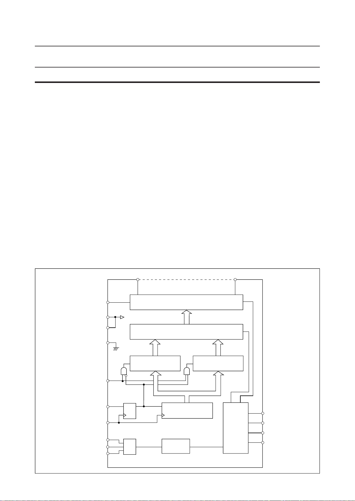
BLOCK DIAGRAM
BLANK
V
DD1
V
DD2
GND
LOAD
DATA
CLOCK
OSC-IN
OSC-C
OSC-R
SEG
1
42-DOT SEGMENT DRIVER
42-BIT SELECTOR
LL
D Q
OSC
<A>
42-BIT LATCH
42-BIT LATCH
42-BIT SI/PO
1/32
<B>
SEG
42
COMMON
DRIVER
COM-A
COM-B
V
LCM
V
LCL
1/12
Page 2
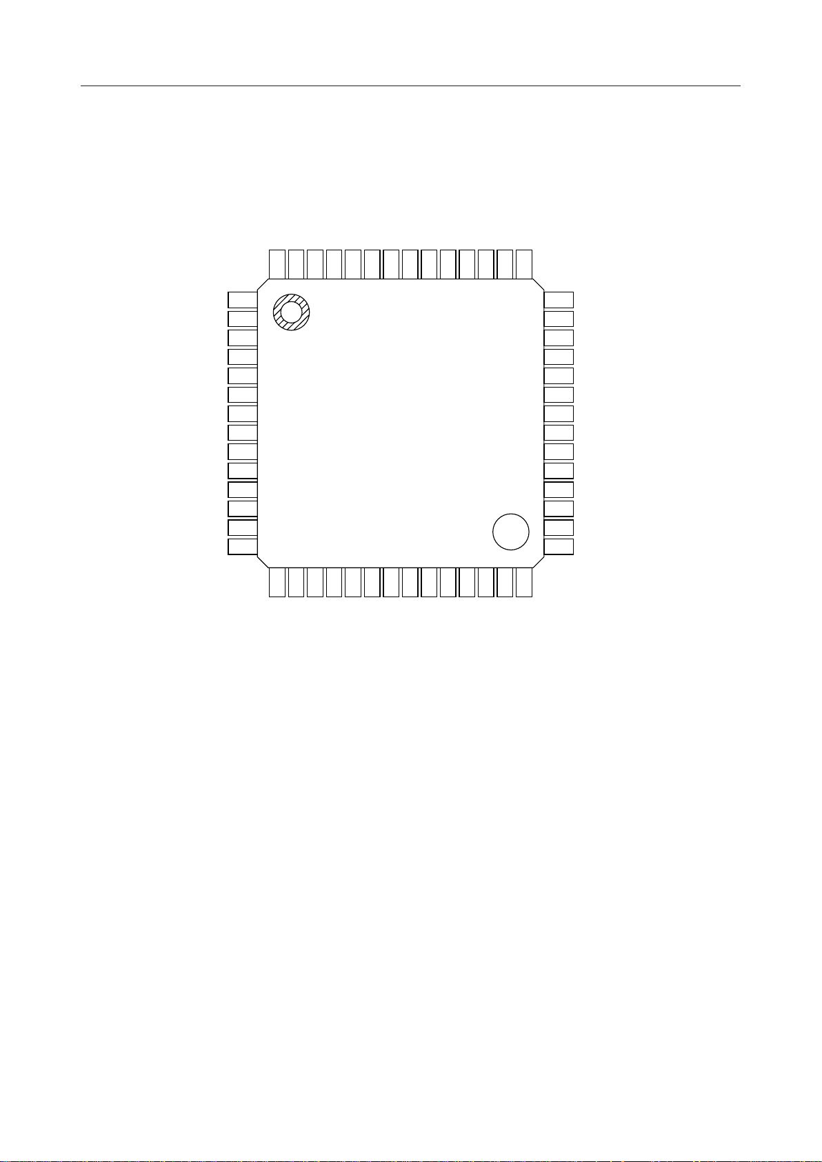
PIN CONFIGURATION (TOP VIEW)
56 SEG28
55 SEG27
54 SEG26
53 SEG25
52 SEG24
51 SEG23
DD2
50 SEG22
49 V
48 SEG21
47 SEG20
46 SEG19
45 SEG1826V
44 SEG1727COM-B
43 SEG1628SEG1
MSM6544¡ Semiconductor
1SEG29
2SEG30
3SEG31
4SEG32
5SEG33
6SEG34
7SEG35
8SEG36
9SEG37
10SEG38
11SEG39
42
41
40
39
38
37
36
35
34
33
32
SEG15
SEG14
SEG13
SEG12
SEG11
SEG10
SEG9
SEG8
SEG7
SEG6
SEG5
12SEG40 31 SEG4
13SEG41 30 SEG3
14SEG42 29 SEG2
15OSC-IN
16OSC-C
17OSC-R
18LOAD
19DATA
20CLOCK
21V
22BLANK
23GND
24V
25COM-A
DD1
LCL
LCM
56-Pin Plastic QFP
2/12
Page 3

MSM6544¡ Semiconductor
PIN DESCRIPTIONS
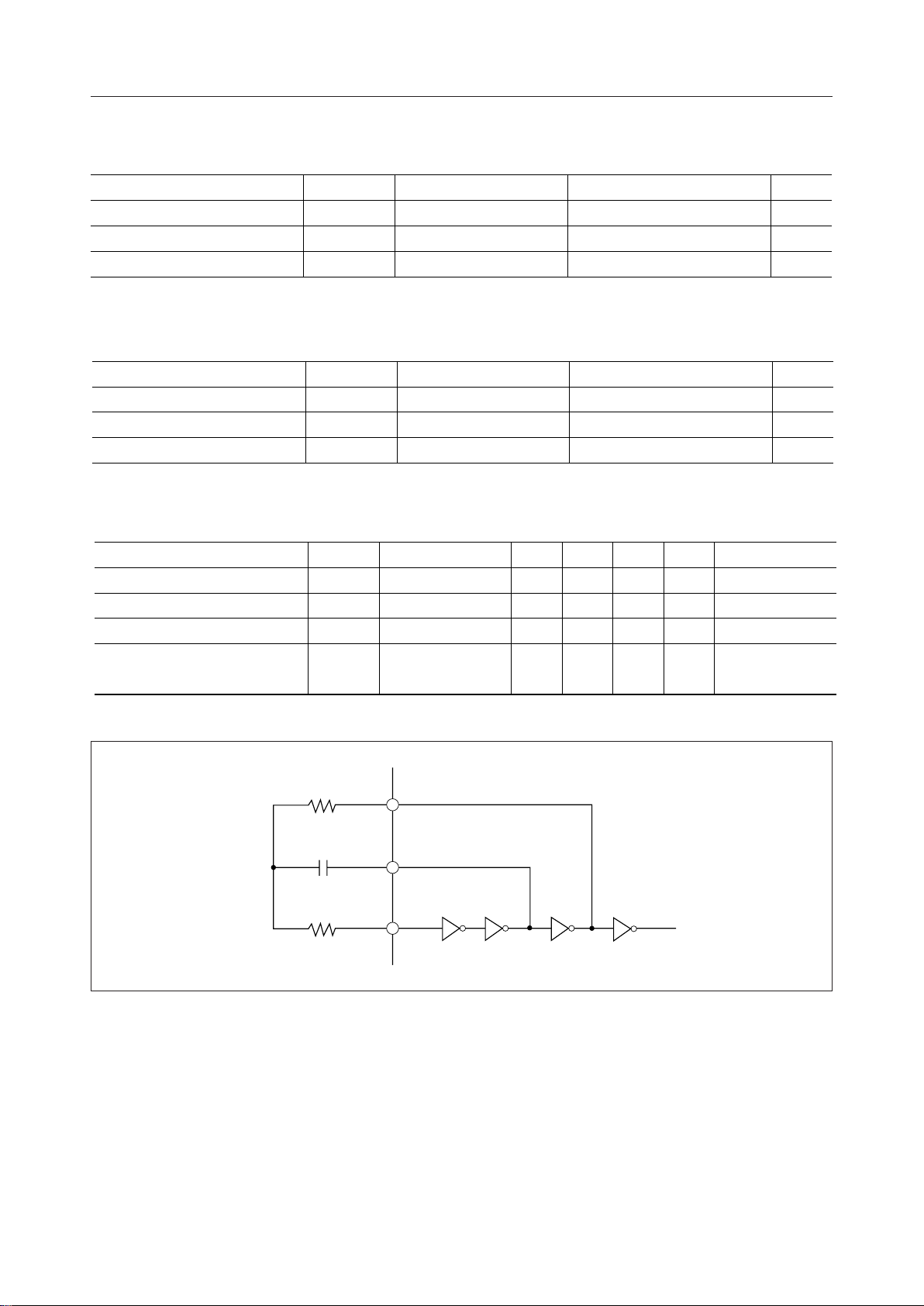
• OSC-IN, OSC-C, OSC-R
An RC oscillator circuit for 3-pin type can be configured. Since the OSC-IN pin is in a high
input impedance state, it is susceptible to noise.
• DATA-IN
This is the display data input. When this pin is at "H" level, the segments are turned on and
when at "L" level, the segments are turned off.
• CLOCK
Pin for clocking display data in. Display data is shifted on the rising edge of the clock pulse.
• LOAD
This is the signal for latching the shift register data. When this pin is set at a "H" level, the shift
register data is transmitted to LATCH <A> or LATCH <B>.
• SEG1 - SEG42
These pins drive the LCD segments.
• COM-A, COM-B
These pins drive the LCD commons. COM-A and COM-B correspond to LATCH <A> output
and LATCH <B>output, respectively.
•V
DD2
This is connected to the V
•V
LCM
pin internally.
DD1
This is the center bias pin of the LCD. Supply the middle voltage between VDD and V
•V
LCL
This is the power supply pin of the LCD driver. The contrast of the LCD can be adjusted by
changing the voltage at this pin, but do not set the voltage less than the GND level.
• BLANK
This pin is used to test the all segment outputs (SEG1 to SEG42). All segment outputs are
turned off when this pin is set to "H" level. The display returns to the condition before the pin
was set to "H" level.
•V
DD1
, GND
These are power supply voltage and ground pins.
LCL
.
3/12
Page 4
ABSOLUTE MAXIMUM RATINGS
Parameter Symbol Condition Rating Unit
Supply Voltage
Input Voltage
Storage Temperature
T
V
DD
V
STG
I
T
= 25°C
a
T
= 25°C
a
—
RECOMMENDED OPERATING CONDITIONS
Parameter Symbol Condition Range Unit
Supply Voltage
Operating Temperature
LCD Driving Voltage
OSC Circuit
V
DD
T
op
V
LCD
—
—
V
DD–VLCL
–0.3 to +6.5 V
GND–0.3 to VDD +0.3
–55 to +150
3 to 6 V
–40 to +85
3 to V
DD
MSM6544¡ Semiconductor
V
°C
°C
V
Parameter Min.
Symbol Condition Typ. Max. Unit Applicable Pin
Oscillation Resistance
Oscillation Capacitance 0.001C
Current Control Resistance 33R
Common Signal Frequency 25f
R
0
C
0
R
1
0
0
1
COM
OSC-R
OSC-C
OSC-IN
— — 68 kW OSC-R
10R
Film capacitor — 0.047 mF OSC-C
— — 220 kW OSC-IN
COM-A
— — 250 Hz
COM-B
(MSM6544)
4/12
Page 5

ELECTRICAL CHARACTERISTICS
DC Characteristics
(V
= 5.0V
DD
MSM6544¡ Semiconductor
Ta = –40 to +85°C)
Parameter Symbol Condition
"H" Input Voltage
V
IH
Corresponding
Pin
BLANK
LOAD
IL
DATA
CLOCK
OSC-IN
Input Leakage Current
I
LI
OSC-R
OSC-C
"H" Output Voltage
V
OH
All segment
outputs
COM-A
COM-B
"M" Output Voltage
V
OM
COM-A
COM-B
OSC-R
OSC-C
Min.
Typ. Max. Unit
—
—
3.6 — V
GND — 1.0 V"L" Input Voltage V
DD
V
VI = 5.0V/0V — — ±1 mA
I
= –200mA 4.5 — — V
O
V
= 2.5V
LCM
V
= 0V
LCL
I
= –30mA
O
= 2.5V
V
LCM
V
= 0V
LCL
I
= –150mA
O
= 2.5V
V
LCM
V
= 0V
LCL
I
= ±150mA
O
= 200mA — — 0.5 V
I
O
4.8 — — V
4.8 — — V
2.3 — 2.7 V
"L" Output Voltage
Segment Output
Impedance
Common Output
Impedance
Static Supply Current
Dynamic Supply Current
R
R
V
COM
I
DD1
I
DD2
OL
SEG
All segment
outputs
COM-A
COM-B
All segment
outputs
COM-A
COM-B
V
DD
V
= 2.5V
LCM
V
= 0V
LCL
I
= 30mA
O
= 2.5V
V
LCM
V
= 0V
LCL
I
= 150mA
O
V
= (5+V
V
V
V
LCM
LCL
LCM
LCL
= 0 to 2V
= 0 to 2V
= (5+V
LCL
LCL
Fix all inputs to
V
or GND
DD
No load
= 47kW
R
o
= 0.0047mF
C
o
=150kW
R
1
)/2
)/2
— — 0.2 V
— — 0.2 V
— — 10 kW
— — 1.5 kW
— — 100 mA
— 0.22 0.5 mA
5/12
Page 6

Switching Characteristics
MSM6544¡ Semiconductor
Parameter Symbol Condition
Clock Pulse Frequency
Clock Pulse "H" Time t
Clock Pulse "L" Time t
Data Setup Time t
Data Hold Time t
Load Pulse "H" Time t
Clock-Load Timing t
OSC-IN Input Frequency f
V
DATA-IN
H
V
L
t
CLOCK
V
L
f
fH
fL
D-f
f-D
f-L
OSC
fL
f
L
t
D-f
Corresponding
V
H
V
L
V
H
V
L
Pin
CLOCK
DATA
CLOCK
LOAD
LOAD
OSC-IN
t
f-D
t
fH
= 3.0 to 6.0V,
(V
DD
—
—
—
—
—
—
—
—
V
H
Ta = –40 to +85°C)
Min.
Max. Unit
— 4 MHz
100 — ns
100 — ns
80 — ns
40 — ns
100 — ns
100 — ns
— 20 kHz
LOAD
t
f-L
t
L
V
H
V
L
(V
H
V
H
= 0.8 VDD, VL = 0.2 VDD)
6/12
Page 7

Data Input Timing
• DATA input timing for COM-A
MSM6544¡ Semiconductor
Invalid data
DATA
–– –– –– ––
424140 4321"L"
CLOCK
LOAD
• DATA input timing for COM-B
Invalid data
DATA
–– –– –– ––
424140 4321"H"
CLOCK
LOAD
SEG-DATA
(A)
SEG-DATA
(B)
SEL
SEL
LOAD
LOAD
Output Waveforms
COM-A
COM-B
SEG
off
off
n
on
off
on
off
off
off
on
off
on
off
COM-A
COM-B
V
V
V
V
V
V
DD
LCM
LCL
DD
LCM
LCL
on
on
on
on
7/12
Page 8

MSM6544¡ Semiconductor
FUNCTIONAL DESCRIPTION
Data Input
The data input consists of the following three timing sections:
i) SEG-DATA section (42-bit)
ii) SEL bit section (1-bit)
iii) LOAD section
A total of 43 bits of 42-bit segment data and 1-bit select bit are taken in the 43-bit shift register
at the rising edge of the clock.
The segment data corresponds to "L" (segment OFF) and "H" (segment ON). Input the
segment data from SEG42 to SEG1 in this order.
The select bit following the segment data is a bit used to specify the transmit destination of
the segment data. The selection is performed as follows.
"L" : LATCH <A> ; corresponds to COM-A
"H" : LATCH <B> ; corresponds to COM-B
The data from the shift register to LATCH <A> or LATCH <B> is transmitted when the LOAD
pin is at the "H" level.
The indication corresponding to the transmit destination latch is also changed at the same
time that data is transmitted.
8/12
Page 9

APPLICATION CIRCUITS
MSM6544¡ Semiconductor
From Controller
COM-B
COM-A
R
x 2
COM
42
V
LCM
V
DD
R
LC
COM-A
R
COM-B
V
LCL
LC
BLANK
LOAD
DATA
LCD PANEL
1/2 DUTY 84-SEGMENT
SEG
1
MSM6544
SEG
CLOCK
V
DD1
V
DD
GND OSC-IN OSC-C OSC-R
R
1
C
0
V
LCL
R
0
>
1kW
R
=
COM
>
R
R
x 3
=
1
o
9/12
Page 10

REFERENCE DATA
MSM6544¡ Semiconductor
I
DD2
vs. V
I
DD2
mA
400
Requirements
300
200
100
01 2 34 567V
• At no lead and during oscillation
• At room temperature
= 47 kW
• R
0
= 0.0047 mF
• C
0
= 150 kW
• R
1
Characteristic
DD
V
DD
10/12
Page 11

MSM6544¡ Semiconductor
f
COM
f
COM
vs. V
Characteristics
DD
Hz
60
Requirements
• At room temperature
= 47 kW
• R
0
= 0.0047 mF
• C
55
50
COM-A
0
= 150 kW
• R
1
COM-B
45
1/f
COM
01 2 3 4 5 6 7V
V
DD
f
COM
R
f
COM
vs.
Characteristics
0
Hz
320
240
160
120
80
60
40
30
20
15
Requirements
• At room temperature
10
• VDD = 5.0 kW
.
• R1 = 3R
.
0
= 0.047mF
0
0101522334768kW
R
0
C
= 0.001mF
0
= 0.0022mF
C
0
C
= 0.0047mF
0
C
= 0.01mF
0
C
= 0.022mFC
0
11/12
Page 12

PACKAGE DIMENSIONS
QFP56-P-910-0.65-2K
Mirror finish
MSM6544¡ Semiconductor
(Unit : mm)
Package material
Lead frame material
Pin treatment
Solder plate thickness
Package weight (g)
Epoxy resin
42 alloy
Solder plating
5 mm or more
0.36 TYP.
Notes for Mounting the Surface Mount Type Package
The SOP, QFP, TSOP, SOJ, QFJ (PLCC), SHP and BGA are surface mount type packages, which
are very susceptible to heat in reflow mounting and humidity absorbed in storage.
Therefore, before you perform reflow mounting, contact Oki’s responsible sales person for the
product name, package name, pin number, package code and desired mounting conditions
(reflow method, temperature and times).
12/12
 Loading...