

Page 1
RF & MICROWAVE TRANSISTORS
.REFRACTORY/GOLD METALLIZATION
.EMITTER BALLASTED
.VSWR CAPABILITY
CONDITIONS
.HERMETIC STRIPAC
.P
= 4.5 W MIN. WITH 4.5 dB GAIN
OUT
@ 3.0 GHz
:1 @ RATED
∞
PACKAGE
ORDER CO DE
MSC83305
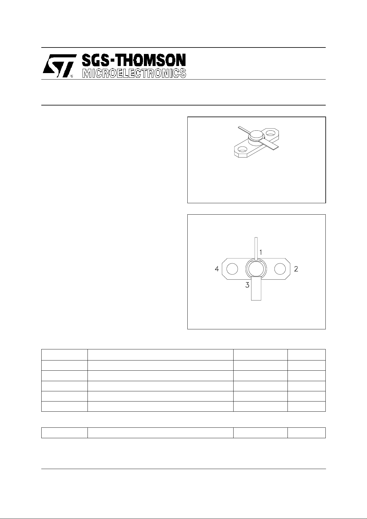
PIN CONNECTION
MSC83305
GENERAL PURPOSE AMPLIFIER APPLICATIONS
.250 2LFL (S010)
hermetically sealed
BRANDING
83305
DESCRIPTION
The MSC83305 is a common base hermetically
sealed silicon NPN microwave power transistor
utilizing an emitter site ballasted geometry with a
refractory gold metallization system. This device
is capable of withstanding an infinite load VSWR
at any phase angle under rated conditions. The
MSC83305 was design ed for Cla ss C ampli fi er/os cillator applications in the 1.0 - 3.0 GHz frequency
range.
ABSOLUTE MAXIMUM RATINGS (T
Symbol Parameter Value Unit
P
DISS
I
C
V
CC
T
J
T
STG
THERMAL DATA
R
TH(j-c)
*Applies only to rated RF amplifier operation
Power Dissipation* (TC ≤ 50˚C) 17.6 W
Device Current* 700 mA
Collector-Supply Voltage* 30 V
Junction Temperature 200
Storage Temperature
Junction-Case Thermal Resistance* 8.5
case
= 25°C)
1. Collector 3. Emitter
2. Base 4. Base
65 to +200
−
°
°
°
C/W
C
C
October 1992
1/5
Page 2
MSC83305
ELECTRICAL SPECIFICATIONS (T
case
= 25°C)
STATIC
Symbol Test Condi tions
BV
BV
BV
I
CBO
h
CBO
EBO
CER
FE
IC = 1mA IE = 0mA 45 — — V
IE = 1mA IC = 0mA 3.5 — — V
IC = 5mA RBE = 10Ω 45 — — V
VCB = 28V — — 0 .5 mA
VCE = 5V IC = 500mA 30 — 300 —
Min. Typ. Max.
Valu e
DYNAMIC
Symbol Test Conditi ons
P
OUT
η
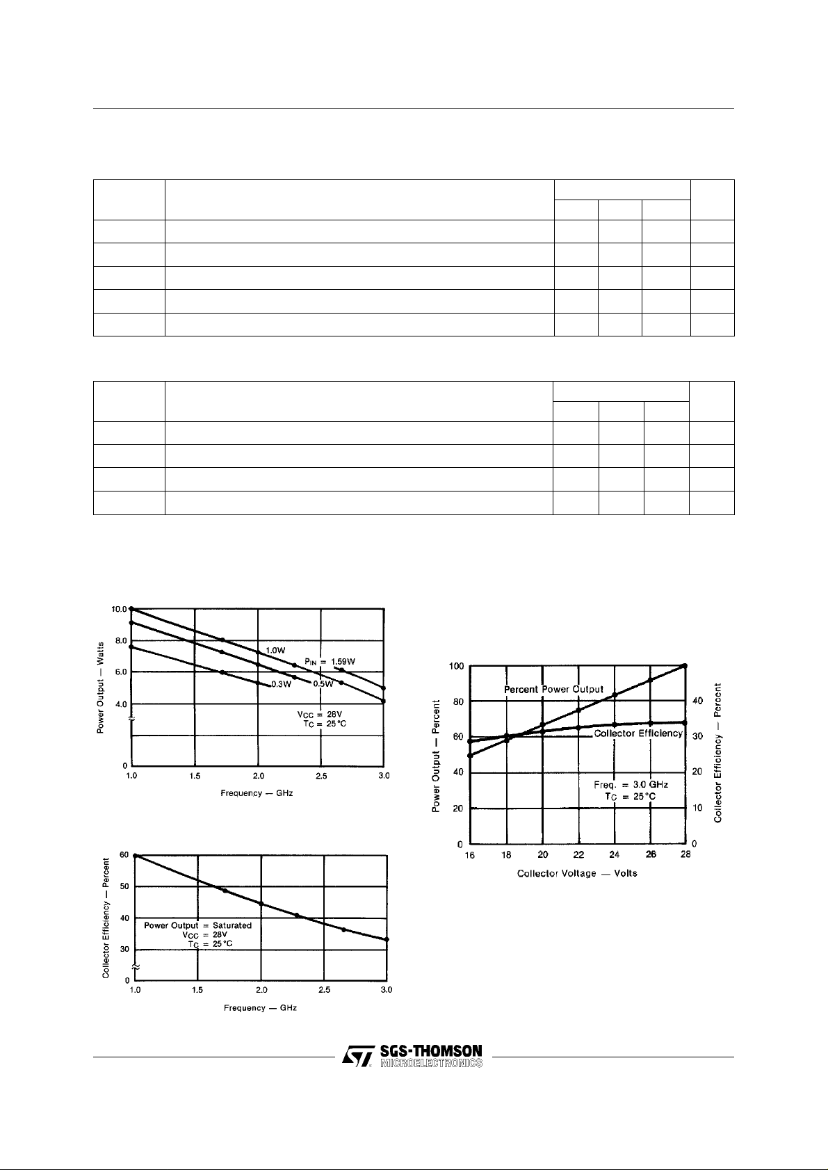
cf = 3.0 GHz PIN = 1.59 W VCC = 28 V 30 33 — %
G
P
C
OB
f = 3.0 GHz PIN = 1.59 W VCC = 28 V 4.5 5.0 — W
f = 3.0 GHz PIN = 1.59 W VCC = 28 V 4.5 5.0 — dB
f = 1 MHz VCB = 28 V — — 7.5 pF
Value
Min. Typ. Max.
Unit
Unit
TYPICAL PERFORMANCE
POWER OUTPUT vs FREQUENCY
COLLECTOR EFFICIENCY vs FREQUENCY
PERCENT POWER OUTPUT & COLLECTOR
EFFICIENCY vs COLLECTOR VOLTAGE
2/5
Page 3
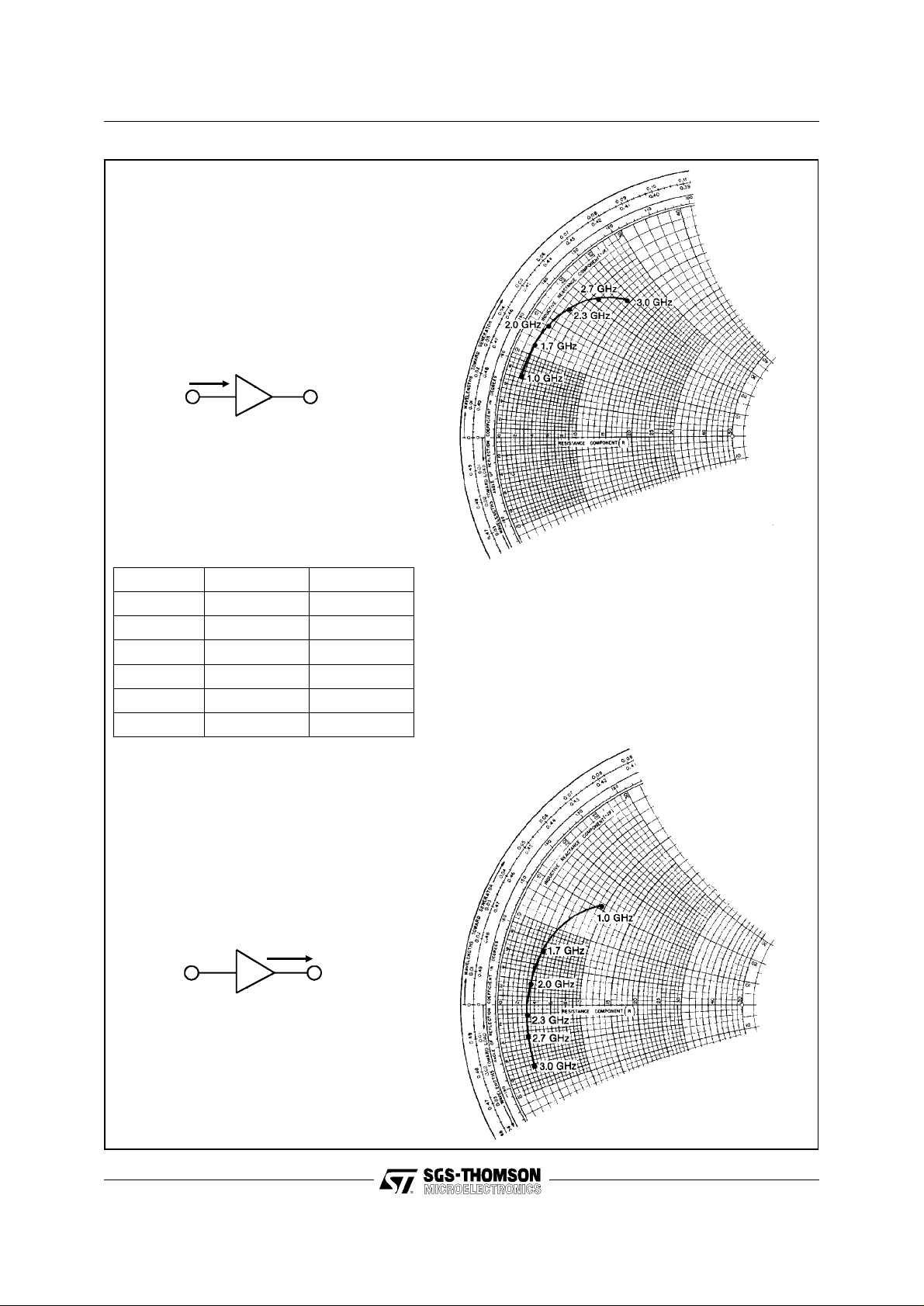
IMPEDANCE DATA
TYPICAL INPUT
IMPEDANCE
Z
IN
MSC83305
FREQ. ZIN (Ω)Z
CL
(Ω)
1.0 GHz 1.7 + j 7.2 9.5 + j 15.5
1.7 GHz 2.0 + j 11.2 4.2 + j 6.7
2.0 GHz 2.4 + j 14.0 3.5 + j 2.5
2.3 GHz 3.6 + j 17.4 3.1 − j 1.2
2.7 GHz 6.0 + j 21.0 3.0 − j 3.8
3.0 GHz 9.5 + j 24.0 3.0 − j 7.2
TYPICAL COLLECTOR
LOAD IMPEDANCE
Z
CL
P
= Saturated
OUT
VCC = 28V
Normalized to 50 ohms
3/5
Page 4

MSC83305
TEST CIRCUIT
Ref.: Dwg. No. C125562
RF Amplifier Power Output Test
PACKAGE MECHANICAL DATA
All dimensions are in inches.
Frequency 3.0 GHz
4/5
Page 5

MSC83305
Information furnished is believed to be accurate and reliable. However, SGS-THOMSON Microelectronics assumes no responsability for the
consequences of use of such information nor for any infringement of patents or other rights of third parties which may results from its use. No
license is granted by implication or otherwise under any patent or patent rights of SGS-THOMSON Microelectronics. Specifications mentioned
in this publication are subject to change without notice. This publication supersedes and replaces all information previously supplied.
SGS-THOMSON Microelectronics products are not authorized for use as critical components in life support devices or systems without express
written approval of SGS-THOMSON Microelectonics.
© 1994 SGS-THOMSON Microelectronics - All Rights Reserved
Australia - Brazil - France - Germany - Hong Kong - Italy - Japan - Korea - Malaysia - Malta - Morocco - The Netherlands -
Singapore - Spain - Sweden - Switzerland - Taiwan - Thailand - United Kingdom - U.S.A
SGS-THOMSON Microelectronics GROUP OF COMPANIES
5/5
 Loading...