

Page 1
RF & MICROWAVE TRAN SIST ORS
GENERAL PURPOSE AMPLIFI ER APPLICAT IONS
.REFRACTORY/GOLD METALLIZATION
.EMITTER SITE BALLASTED
.VSWR CAPABILITY
CONDITIONS
.HERMETIC STRIPAC
. P
OUT
@3.0GHz
1.0 W MIN . WITH 7. 0 dB G AI N
=
:1 @ RATED
∞
PACKAGE
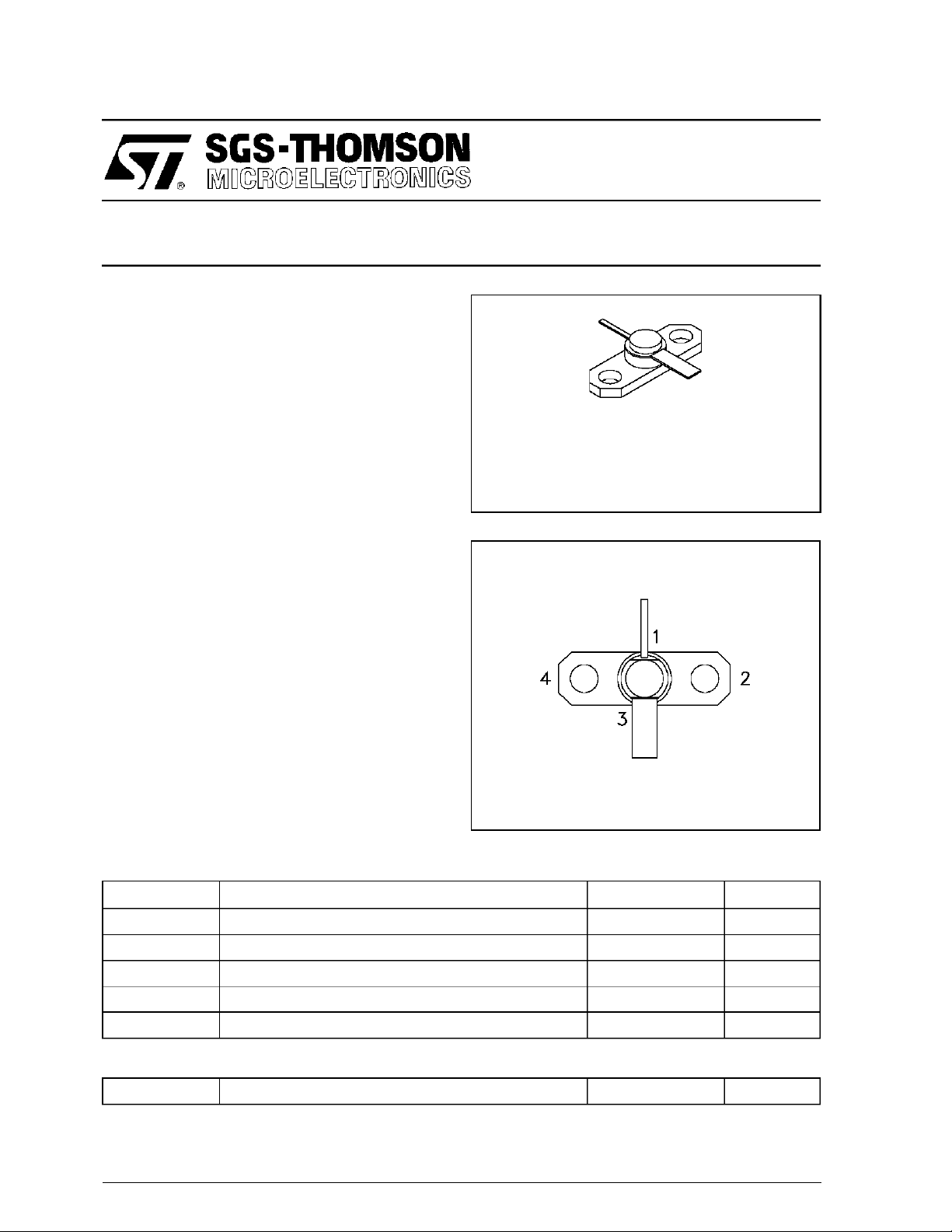
MSC83301
.250 2LF L (S010)
hermetically sealed
ORDER CODE
MSC83301
PIN CONNECTION
DESC RIPTIO N
The MSC83301 is a common base hermetically
sealed silicon NPN microwave power transistor
utilizing an overlay, emitter site ballasted geometry with a refractory gold metallization system.
This device is capable of withstanding an infinite
load VSWR at any phase angle under rated conditions. The MSC83301 is designed for Class C
amplifier/oscillator applications in the 1.0 - 3.0
GHz frequency range.
ABSOLUTE MAXIMUM RATINGS (T
Symbol Parameter Value Uni t
P
T
DISS
I
V
CC
T
STG
C
J
Power Dissipation* (TC≤ 50°C) 6.0 W
Device Current* 200 mA
Collector-Supply Voltage* 30 V
Junction Temperature 200
Storage Temperature − 65 to +200
case
= 25°C)
1. Collector 3. Emitter
2. Base 4. Base
BRANDING
83301
°
C
°
C
THERMA L DATA
R
TH(j-c)
*Appliesonlyto rated RF amplifier operation
September 2, 1994
Junction-Case Thermal Resistance* 25
°
C/W
1/5
Page 2
MS C83 301
ELECTRICAL SPECIFICATIO NS (T
case
= 25°C)
STATIC
Symbol Test Conditions
BV
CBOIC
BV
EBOIE
BV
CERIC
I
CBO
h
FE
= 1mA IE=0mA 45 — — V
= 1mA IC=0 mA 3.5 — — V
= 5mA RBE= 10 Ω 45 — — V
VCB= 28V — — 0.5 mA
VCE= 5V IC=100 mA 30 — 300 —
DYNAMIC
Symbol Test C onditi ons
P
OUT
η
P
C
OB
f = 3.0 GHz P
cf=3.0 GHz P
f = 3.0 GHz P
G
f = 1 MHz V
0.20 W V
=
IN
0.20 W V
=
IN
0.20 W V
=
IN
28 V — — 3.5 pF
CB =
Value
Min. Typ. Max.
Value
Min. Typ. Max.
28 V 1.0 1.3 — W
=
CC
28 V 33 36 — %
=
CC
28 V 7.0 8.1 — dB
=
CC
Unit
Unit
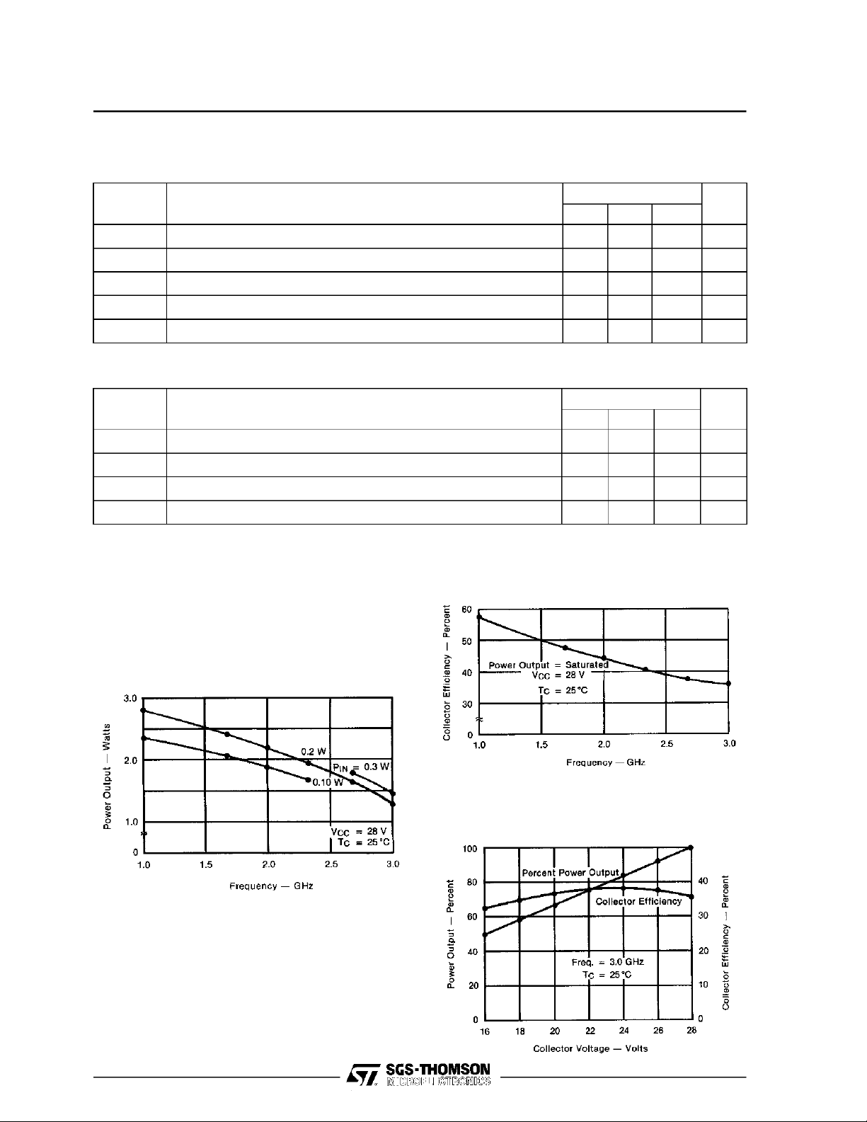
TYPICA L PERFOR MA NCE
TYPICAL POWER OUTPUT vs
FREQUENCY
TYPICAL COLLECTOR
EFFICI ENCY vs FREQ U ENCY
PERCENT POWER OUTPUT & COLLECTOR
EFFICIENCY vs COLLECTOR VOLTAGE
2/5
Page 3

IMPEDA NCE D ATA
TYPICAL I NPUT
IMPEDANCE
Z
IN
MS C833 01
FREQ. ZIN(Ω)Z
CL
(Ω)
1.0 GHz 9.0 + j 9.0 21.0 + j 48.0
1.7 GHz 9.5 + j 23.0 12.0 + j 32.0
2.0 GHz 18.0 + j 34.5 7.5 + j 22.0
2.3 GHz 28.0 + j 41.0 5.0 + j 13.0
2.7 GHz 49.0 + j 39.0 4.0 + j 7.0
3.0 GHz 65.0 + j 22.0 3.8 + j 3.0
TYPICAL COLLECTOR
LOAD IMPEDANCE
Z
CL
P
OUT =
V
CC
Saturated
28 V
=
Normalized to 50 ohms
3/5
Page 4

MS C83 301
TEST CIRCUIT
RF Amplifier Power Output Test
All dimensions are in inches. Ref.: Dwg. No. C125518
4/5
Page 5

PACKAGE MECHANICAL DATA
Ref.: Dwg. No. 12-0216 rev. A
MS C833 01
Information furnished is believed to be accurate and reliable. However, SGS-THOMSON Microelectronics assumes no responsibility
for the consequences of use of such information nor for any infringement of patents or other rights of third parties which may result
from its use. No license is granted by implication or otherwise under any patent or patent rights of SGS-THOMSON Microelectronics. Specifications mentioned in this publication are subject to change without notice. This publication supersedes and replaces all
information previously supplied. SGS-THOMSON Microelectronics products are not authorized for use as critical components in life
support devices or systems without express written approval of SGS-THOMSON Microelectronics.
1994 SGS-THOMSON Microelectronics - All Rights Reserved
Australia - Brazil - France - Germany - Hong Kong - Italy - Japan - Korea - Malaysia - Malta - Morocco - The Netherlands -
Singapore - Spain - Sweden - Switzerland - Taiwan - Thailand - United Kingdom - U.S.A.
SGS-THOMSON Microelectronics GROUP OF COMPANIES
5/5
 Loading...