

Page 1
RF & MICROWAVE TRANSIST ORS
GENERAL PURPOSE LINEAR APPLICA TIONS
.EMITT ER BALLASTED
. CLASS A LINEAR OPERATION
. CO MMON EMITTER
.VSW R CAPABILITY
CONDITIONS
:1 @ RATED
∞
.ft 1.6 GHz TYPICAL
.NOISE FIGURE 15.5 d B @ 2 GHz
.P
OUT
27 dBm MIN. @ 1.0 GHz
=
ORDER CODE
MSC82100
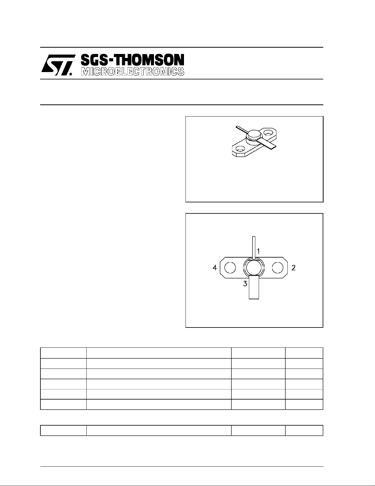
PIN CONNECTION
MSC82100
.250 2LFL (S011)
hermetically sealed
BRANDING
82100
DESC RIPT ION
The MSC82100 is a hermetically sealed NPN
power transistor with a fishbone, emitter finger
ballasted geometry utilizing a refractory/gold metallization system. The device is designed specifically for Class A linear applications to provide
high gain and high output power at the 1.0 dB
compression point.
ABSOLUTE MAXIMUM RATINGS (T
Symbol Parameter Value Uni t
P
DISS
I
C
V
CE
T
J
T
STG
THERMA L DATA
R
TH(j-c)
*Appliesonly to ratedRF amplifieroperation
Power Dissipation (see Safe Area) — W
Device Bias Current 200 mA
Collector-Emitter Bias Voltage* 20 V
Junction Temperature 200
Storage Temperature − 65 to +200
Junction-Case Thermal Resistance* 20
case
= 25°C)
1. Collector 3. Base
2. Emitter 4. Emitter
°
°
°
C/W
C
C
October 1992
1/6
Page 2

MS C82100
ELECTRICAL SPECIFICATIO NS (T
case
= 25°C)
STATIC
Symbol Test Conditions
BV
BV
BV
I
CBO
EBO
CEO
CEO
h
FE
IC= 1mA IE= 0mA 45 — — V
IE= 1mA IC= 0mA 3.5 — — V
IC = 5mA IB= 0mA 20 — — V
VCE= 18V — — 0.5 mA
VCE= 5V IC= 100mA 15 — 120 —
DYNAMIC
Symbol Test Conditi ons
GP*f=1.0 GHz P
∆GP*f=1.0 GHz P
C
OB
* Note: V
f = 1 MHz V
18V
=
CE
I
100mA
=
C
27 dBm 10.5 11.5 — dB
=
OUT
27 dBm
=
OUT
28 V — — 3.2 pF
=
CB
Value
Min. Typ. Max.
Value
Min. Typ. Max.
P
∆
= 10 dB — — 1 dB
OUT
Unit
Unit
2/6
Page 3

TYPICA L PERFORMA NCE
TYPICAL POWER OUTPUT & GAIN @ 1dB
COMPRESSION POI NT vs FREQUENCY
MS C82100
TYPICAL POWER OUTPUT & GAIN @
1dB CO MPRESSION POINT vs
COLLECTOR CURRENT
MAXIMUM OPERATING AREA FOR
FORWARD BIAS OPERATION
TYPICAL LINEAR GAIN vs
COLLECTOR CURRENT
3/6
Page 4

MS C82100
TYPICAL S−PARA METER S
V
18 V
CE =
I
100 mA
=
C
Zg = 50 ohms
4/6
Page 5

TEST CIRCUIT
Ref.: Dwg. No. C127323
All dimensions are in inches.
Frequency 1.0 GHz
MS C82100
PACKAGE MECHANICAL DATA
5/6
Page 6

MS C82100
Information furnished is believed to be accurate and reliable.However, SGS-THOMSON Microelectronics assumes no responsability for the
consequences of use of such information nor for any infringementofpatents or other rights of third parties which may results from its use. No
license isgranted by implication orotherwise underany patentorpatent rights ofSGS-THOMSON Microelectronics. Specificationsmentioned
in this publication are subject to changewithout notice. This publication supersedes andreplaces all information previously supplied.
SGS-THOMSON Microelectronicsproductsare notauthorized foruse ascritical componentsinlife supportdevices or systemswithout express
written approval of SGS-THOMSON Microelectonics.
1994 SGS-THOMSON Microelectronics - All RightsReserved
Australia - Brazil - France - Germany - Hong Kong - Italy - Japan - Korea - Malaysia - Malta - Morocco - The Netherlands -
Singapore - Spain - Sweden - Switzerland - Taiwan - Thailand - United Kingdom - U.S.A
SGS-THOMSON MicroelectronicsGROUP OF COMPANIES
6/6
 Loading...