

Page 1
RF & MICROWAVE TRAN SIST ORS
GENERAL PURPOSE AMPLIFI ER APPLICAT IONS
.EMITT ER BALLASTED
. REFRACTORY/GOLD METALLIZATION
.VSWR CAPABILITY
CONDITIONS
.HERMETIC STRIPAC
. P
OUT
@2.0GHz
1.0 W MIN. WITH 7. 0 dB GAIN
=
:1 @ RATED
∞
PACKAGE
ORDER CODE
MSC82001
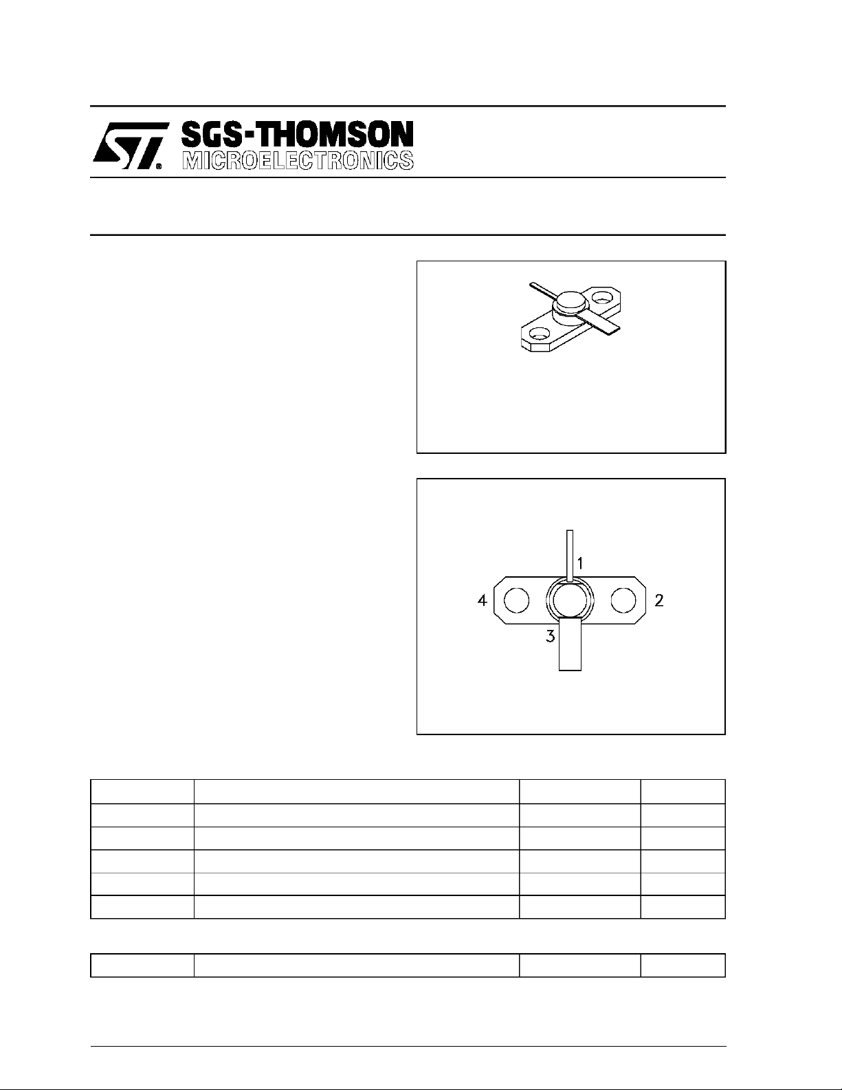
PIN CONNECTION
MSC82001
.250 2LFL (S010)
hermetically sealed
BRANDING
82001
DESCRIPTIO N
The MSC82001 is a common base hermetically
sealed silicon NPN microwave transistor utilizing
a fishbone emitter ballasted geometry with a refractory/gold metallization system. This device is
capable of withstanding an infinite load VSWR at
any phase angle under rated rated conditions. The
MSC82001 was designed for Class C amplifier
applications in the 1.0 - 2.0 GHz frequency range.
ABSOLUTE MAXIMUM RATINGS (T
Symbol Parameter Value Uni t
P
DISS
I
C
V
CC
T
J
T
STG
THERMA L DATA
R
TH(j-c)
*Appliesonly to ratedRF amplifier operation
Power Dissipation* 7.0 W
Device Current* 200 mA
Collector-Supply Voltage* 35 V
Junction Temperature 200
Storage Temperature − 65 to +200
Junction-Case Thermal Resistance* 20
case
= 25°C)
1. Collector 3. Emitter
2. Base 4. Base
°
°
°
C/W
C
C
October 1992
1/5
Page 2
MS C82001
ELECTRICAL SPECIFICATIONS (T
case
= 25°C)
STATIC
Symbol Test Conditions
BV
BV
BV
I
CBO
EBO
CER
CBO
h
FE
IC= 1mA IE= 0mA 45 — — V
IE= 1mA IC= 0mA 3.5 — — V
IC = 5mA RBE= 10Ω 45 — — V
VCB= 28V — — 0.5 mA
VCE= 5V IC= 100mA 15 — 120 —
DYNAMIC
Symbol Test Conditi ons
P
OUT
η
cf=2.0 GHz P
G
P
C
OB
f = 2.0 GHz P
f = 2.0 GHz P
f = 1 MHz V
0.2 W V
IN =
0.2 W V
=
IN
0.2 W V
=
IN
28 V — — 3.2 pF
=
CB
Value
Min. Typ. Max.
Value
Min. Typ. Max.
28 V 1.0 1.2 — W
CC =
28 V 35 40 — %
=
CC
28 V 7.0 7.8 — dB
=
CC
Unit
Unit
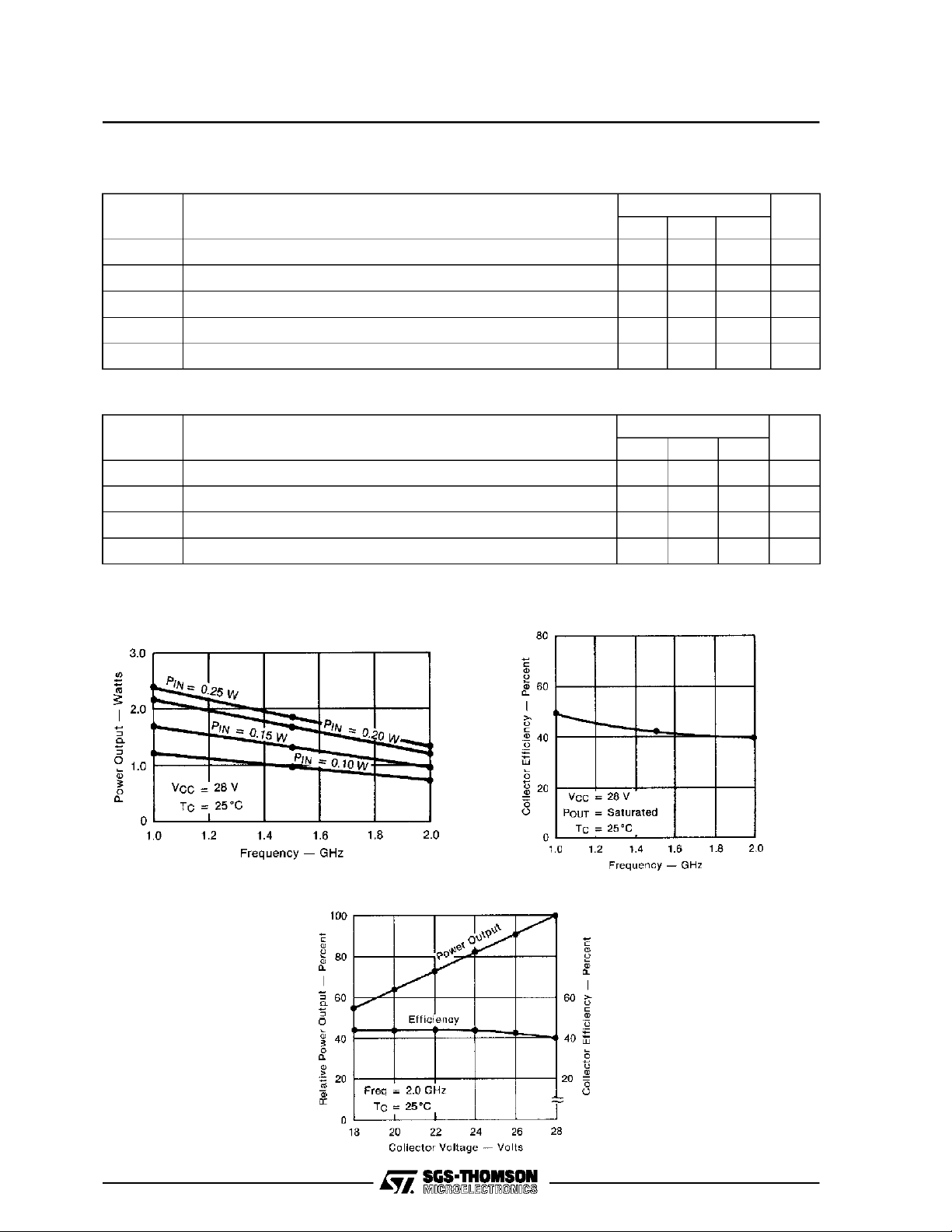
TYPICA L P ERFO R MANCE
POWER OUTPUT vs FREQUENCY
COLLECTOR EFFICIENCY vs
FREQUENCY
RELATIVE POWER OUTPUT vs
COLLECTOR VOLTAGE
2/5
Page 3

IMPEDA NCE DATA
TYPI CAL INPUT
IMPEDANCE
Z
IN
P
0.2 W
=
IN
V
28 V
=
CC
Normalized to 50 ohms
MS C82001
TYPICAL COLLECTOR
LOAD IMPEDANCE
Z
CL
P
V
OUT
CC
Saturated
=
28 V
=
Normalized to 50 ohms
FREQ. ZIN(Ω)Z
CL
(Ω)
1.0 GHz 8.3 + j 7.0 18.0 + j 38.0
1.5 GHz 12.0 + j 16.0 9.6 + j 30.0
1.7 GHz 15.0 + j 14.0 7.0 + j 22.0
2.0 GHz 21.5 + j 22.5 5.0 + j 12.0
3/5
Page 4

MS C82001
TEST CIRCUIT
Ref.: Dwg. No. C127
RF Amplifier Power Output Test
All dimensions are in inches.
Frequency 2.0 GHz
PACKAGE MECHANICAL DATA
4/5
Page 5

MS C82001
Information furnished is believed to be accurate and reliable.However, SGS-THOMSON Microelectronics assumes no responsability for the
consequences of use of such information nor for any infringementofpatents or other rights of third parties which may results from its use. No
license isgrantedby implication orotherwiseunder any patentor patent rights ofSGS-THOMSON Microelectronics. Specificationsmentioned
in this publication are subject to changewithout notice. This publication supersedes and replaces all information previously supplied.
SGS-THOMSON Microelectronicsproductsare notauthorized foruse ascritical componentsin lifesupportdevices orsystems withoutexpress
written approval of SGS-THOMSON Microelectonics.
1994 SGS-THOMSON Microelectronics - All RightsReserved
Australia - Brazil - France - Germany - Hong Kong - Italy - Japan - Korea - Malaysia - Malta - Morocco - The Netherlands -
Singapore - Spain - Sweden - Switzerland - Taiwan - Thailand - United Kingdom - U.S.A
SGS-THOMSON MicroelectronicsGROUPOF COMPANIES
5/5
 Loading...