

Page 1
RF & MICROWAVE TRAN SIST ORS
.REFRACTORY/GOLD METALLIZATION
.EMITTER SITE BALLASTED
.
:1 VSWR CAPABILITY
∞
.LOW THERMAL RESISTANCE
.INPUT MATCHING
.OVERLAY GEOMETRY
.METAL/CERAMIC HERMETIC PACKAGE
.P
OUT =
DESCRI PTIO N
The MSC81035MP is a medium power Class C
transistor designed specifically for pulsed L-Band
avionics applications. This device is a direct replacement for the MSC1035MP. MSC81035MP offers improved saturated ouput power and collector
effic iency based on the test circuit described
herein.
Low RFthermal resistance and computerized automatic wire bonding techniques ensure high reliability and product consistency.
The MSC81035MP ishoused inthe IMPAC package with internal input matching.
35 W MIN . WIT H 10.7 dB G AIN
MSC81035MP
AVIONI CS APPLICAT IONS
.280 4LSL (S 051)
epoxy sealed
ORDER CODE
MSC81035MP
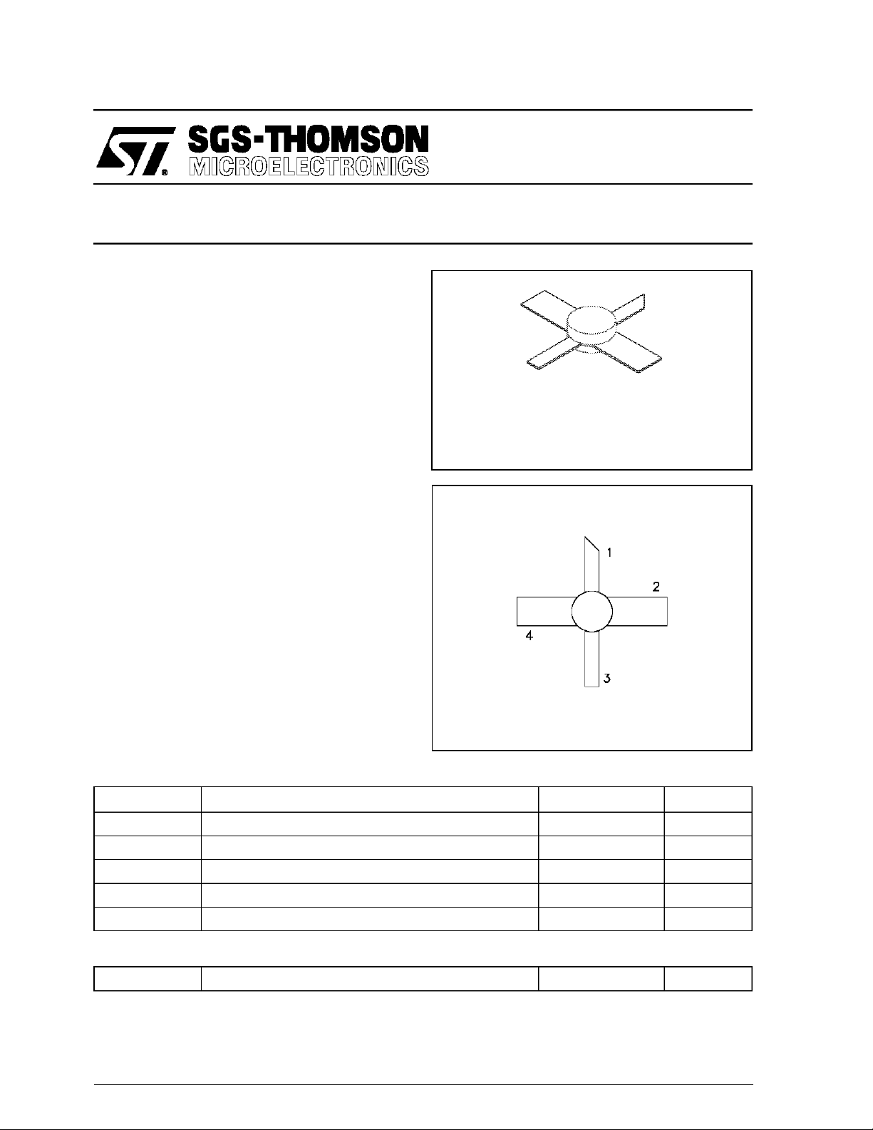
PIN CONNECTION
1. Collector 3. Emitter
2. Base 4. Base
BRANDING
81035MP
ABSOLUTE MAXIMUM RATINGS (T
Symbol Parameter Value Uni t
P
DISS
I
C
V
CC
T
J
T
STG
THERMA L DATA
R
TH(j-c)
*Appliesonlyto rated RF amplifier operation
Note: Thermal Resistancedetermined by Infra-Red Scanning of Hot-Spot
October 1992
Junction Temperature at ratedRF operating conditions.
Power Dissipation* (TC≤ 100°C) 150 W
Device Current* 3.0 A
Collector-Supply Voltage* 55 V
Junction Temperature (Pulsed RF Operation) 250
Storage Temperature
Junction-Case Thermal Resistance* 1.0
case
= 25°C)
65 to +150
−
°
°
°
C/W
C
C
1/4
Page 2
MSC81035MP
ELECTRICAL SPECIFICATIONS (T
case
= 25°C)
STATIC
Symbol Test Conditions
BV
BV
BV
I
CES
h
CBO
EBO
CER
FE
IC= 10mA IE= 0mA 65 — — V
IE= 1mA IC= 0mA 3.5 — — V
IC = 10mA RBE= 10Ω 65 — — V
VBE= 0V VCE= 50V — — 5 mA
VCE= 5V IC= 500mA 15 — 120 —
DYNAMIC
Symbol Test Conditions
P
OUT
η
cf=1025 — 1150 MHz P
G
P
Note: Pulse Width
f = 1025 — 1150 MHz P
f = 1025 — 1150 MHz P
10µSec
=
Duty Cycle=1%
3.0W V
=
IN
3.0W V
=
IN
3.0W V
=
IN
Value
Min. Typ. Max.
Value
Min. Typ. Max.
50V 35 40 — W
=
CC
50V 10.7 11.2 — %
=
CC
50V 43 48 — dB
=
CC
Unit
Unit
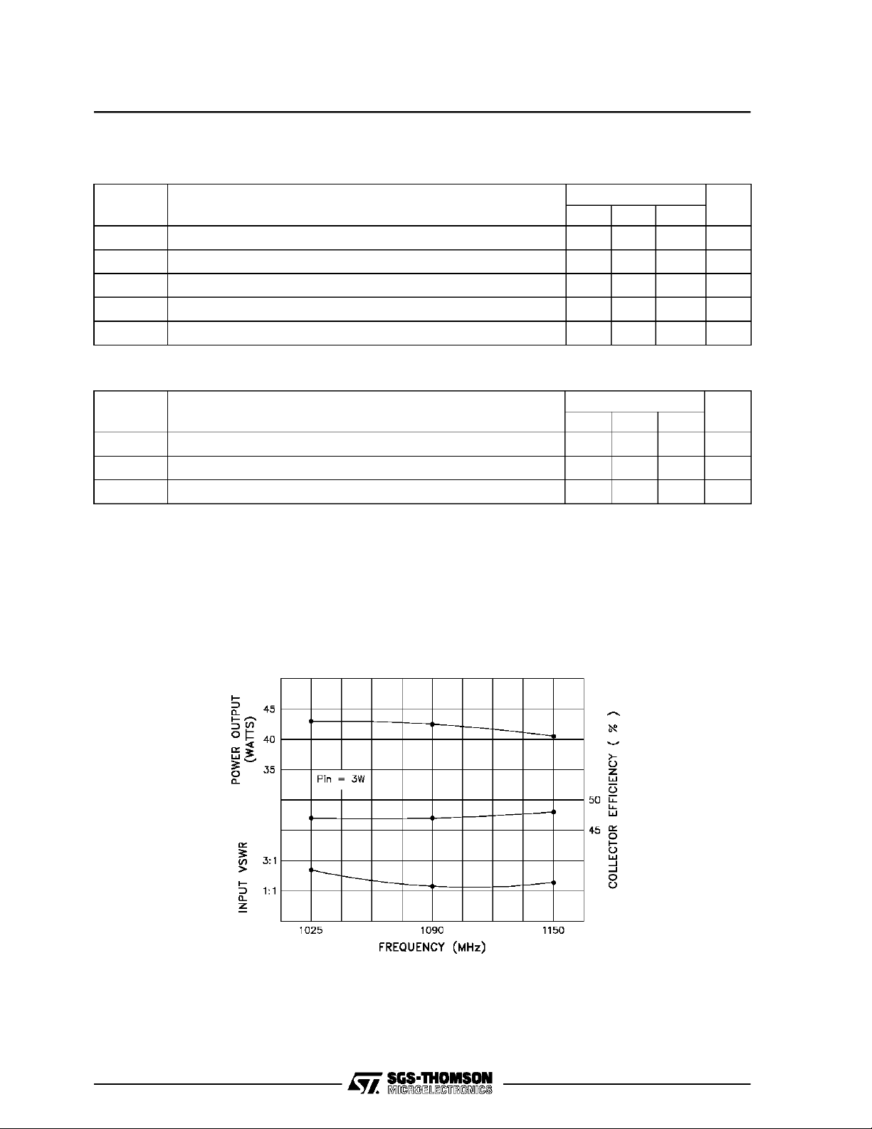
TYPICA L P ERFO R MA NCE
TYPICAL BROADBAND POWER
AMPLIFIER
2/4
Page 3

IMPEDA NCE DATA
TYPICAL I NPUT
IMPEDANCE
Z
IN
TYPICAL COLLECTOR
LOAD I MPEDANCE
MS C810 35 MP
Z
IN
H
M
Z
CL
L
Z
CL
L
M
FREQ. ZIN(Ω)Z
L=1025 MHz 2.6 + j 8.3 7.7 + j 2.0
M=1090 MHz 2.8 + j 8.7 7.1 + j 1.0
H=1150 MHz 3.2 + j 4.4 6.5 − j 0.5
TEST CIRCUIT
Ref.: Dwg. No. 101 002888
CL
(Ω)
H
P
3.0 W
=
IN
V
50 V
CC =
Normalized to 50 ohms
All dimensions are in inches.
3/4
Page 4

MSC81035MP
PACKAGE MECHANICAL DATA
Information furnished is believed to be accurate and reliable.However, SGS-THOMSON Microelectronics assumes no responsability for the
consequences of use of such information nor for any infringementof patents or other rights of third parties which may results from its use. No
license isgranted byimplication or otherwiseunder any patentor patent rights of SGS-THOMSON Microelectronics. Specificationsmentioned
in this publication are subject to changewithout notice. This publication supersedes and replaces all information previously supplied.
SGS-THOMSON Microelectronicsproductsare notauthorized for use ascritical componentsinlife supportdevices orsystemswithout express
written approval of SGS-THOMSON Microelectonics.
1994 SGS-THOMSON Microelectronics - All RightsReserved
Australia - Brazil - France - Germany - Hong Kong - Italy - Japan - Korea - Malaysia - Malta - Morocco - The Netherlands -
Singapore - Spain - Sweden - Switzerland - Taiwan - Thailand - United Kingdom - U.S.A
SGS-THOMSON Microelectronics GROUP OF COMPANIES
4/4
 Loading...