

Page 1
RF & MICROWAVE TRANSISTORS
.EMITTER BALLASTED
.CLASS A LINEAR OPERATION
.COMMON EMITTER
.VSWR CAPABILITY 20:1 @ RATED
CONDITIONS
.ft 3.2 GHz TYPICAL
.NOISE FIGURE 12.0 dB @ 2 GHz
.P
= 28 dBm MIN. @ 2.0 GHz
OUT
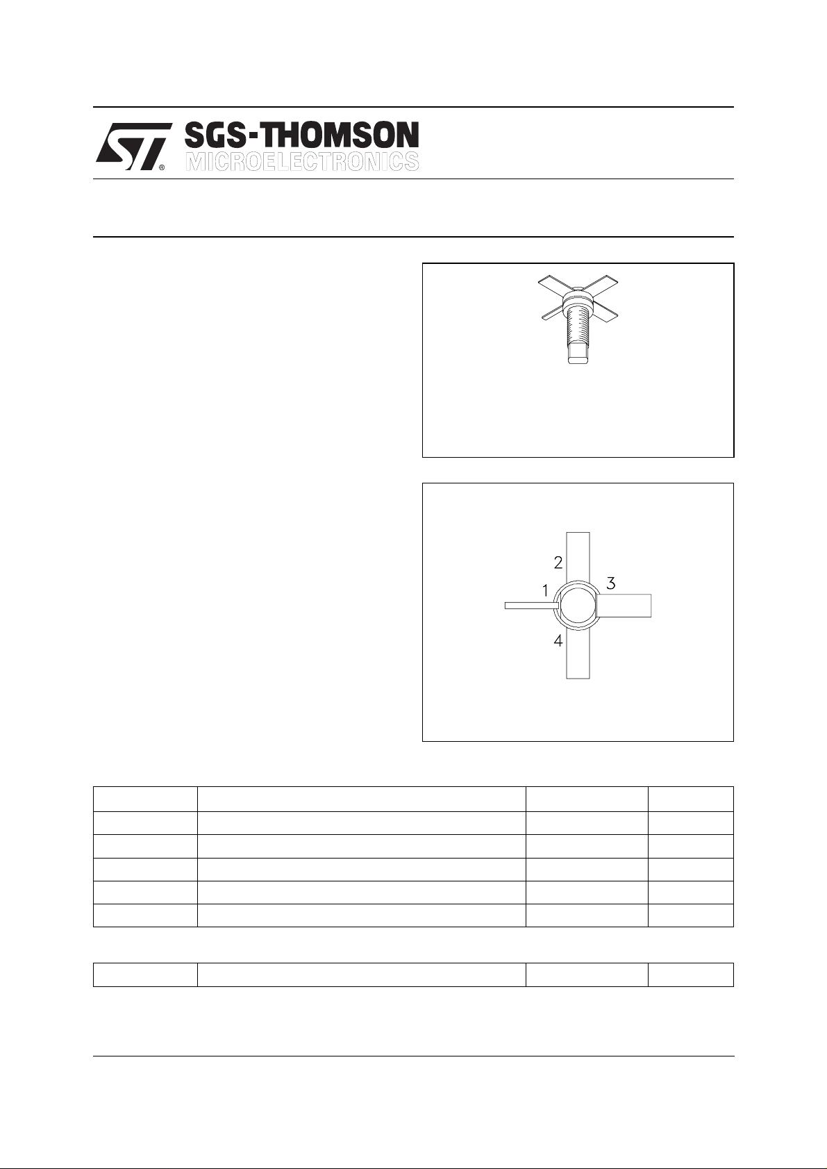
.230 4L STUD (S027)
ORDER CO DE
MSC80185
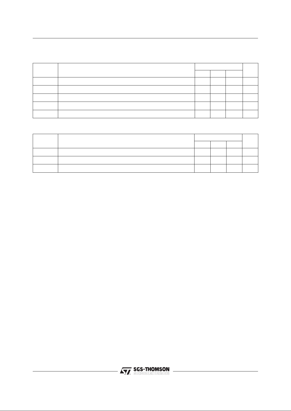
PIN CONNECTION
MSC80185
GENERAL PURPOSE LINEAR APPLICATIONS
hermetical ly sealed
BRANDING
80185
DESCRIPTION
The MSC80185 is a hermetically sealed NPN
power tra nsistor featur ing a unique m atrix struc ture.
This device is specifically designed for Class A
linear applications to provide high gain and high
output power at the 1.0 dB compression point.
ABSOLUTE MAXIMUM RATINGS (T
Symbol Parameter Value Unit
P
DISS
I
C
V
CE
T
J
T
STG
THERMAL DATA
R
TH(j-c)
*Applies only to rated RF amplifier operation
October 1992
Power Dissipation (see Safe Area) — W
Device Bias Current 300 mA
Collector-Emitter Bias Voltage* 20 V
Junction Temperature 200
Storage Temperature
Junction-Case Thermal Resistance* 35
case
= 25°C)
1. Collector 3. Base
2. Emitter 4. Emitter
65 to +200
−
°
°
°
C/W
C
C
1/6
Page 2
MSC80185
ELECTRICAL SPECIFICATIONS (T
case
= 25°C)
STATIC
Symbol Test Condition s
BV
BV
BV
I
CBO
EBO
CEO
CEO
h
FE
IC = 1mA IE = 0mA 50 — — V
IE = 1mA IC = 0mA 3.5 — — V
IC = 5mA IB = 0mA 20 — — V
VCE = 18V — — 0. 5 mA
VCE = 5V IC = 100mA 15 — 120 —
DYNAMIC
Symbol Test Conditions
GP*f = 2.0 GHz P
∆GP*f = 2.0 GHz P
C
OB
* Note: VCE = 18V
f = 1 MHz VCB = 28 V — — 3.0 pF
IC
140mA
=
= 28 dBm 7.5 8.5 — dB
OUT
28 dBm
=
OUT
Valu e
Min. Typ. Max.
Value
Min. Typ. Max.
P
= 10 dB — — 1 d B
∆
OUT
Unit
Unit
2/6
Page 3

TYPICAL PERFORMANCE
TYPICAL POWER OUTPUT & GAIN @ 1dB
COMPRESSION POINT vs FREQUENCY
MSC80185
TYPICAL POWER OUTPUT & GAIN @
1dB COMPRESSION POINT vs
COLLECTOR CURRENT
MAXIMUM OPERATING AREA FOR
FORWARD BIAS OPERATION
TYPICAL LINEAR GAIN vs
COLLECTOR CURRENT
3/6
Page 4

MSC80185
TYPICAL S−PARAMETERS
VCE = 18 V
IC = 140 mA
Zg = 50 ohms
4/6
Page 5

TEST CIRCUIT
Ref.: Dwg. No. C127304A
All dimensions are in inches.
MSC80185
PACKAGE MECHANICAL DATA
5/6
Page 6

MSC80185
Information furnished is believed to be accurate and reliable. However, SGS-THOMSON Microelectronics assumes no responsability for the
consequences of use of such information nor for any infringement of patents or other rights of third parties which may results from its use. No
license is granted by implication or otherwise under any patent or patent rights of SGS-THOMSON Microelectronics. Specifications mentioned
in this publication are subject to change without notice. This publication supersedes and replaces all information previously supplied.
SGS-THOMSON Microelectronics products are not authorized for use as critical components in life support devices or systems without express
written approval of SGS-THOMSON Microelectonics.
© 1994 SGS-THOMSON Microelectronics - All Rights Reserved
Australia - Brazil - France - Germany - Hong Kong - Italy - Japan - Korea - Malaysia - Malta - Morocco - The Netherlands -
Singapore - Spain - Sweden - Switzerland - Taiwan - Thailand - United Kingdom - U.S.A
SGS-THOMSON Microelectronics GROUP OF COMPANIES
6/6
 Loading...