

Page 1
Semiconductor
MSC23V43257D-xxBS8
4,194,304-word x 32-b i t DYNAMIC RAM MODULE : FAST PAGE MODE TYPE WITH EDO
This vers i on: Apr. 13. 1999
DESCRIPTION
The MSC23V43257D-xxBS8 is a 4,194,304-word x 32-bit CMOS dynamic random access memory module which is
composed of ei ght 16Mb(4Mx 4) DRAMs i n TSOP packages m ounted with eight decoupl ing capac itors. Thi s is an
100-pin dual in-line memory module. This module supports any application where high density and large capacity of
storage mem or y ar e r equired.
FEATURES
· 4,194,304-word x 32- bit organization
· 100-pin Dual In-line Memory Module
· Gold tab
· Singl e 3.3V power supply, ±0.3V tolerance
· Input : LVTTL compatible
· Output : LVTTL compatible, 3-state
· Refresh : 2048cycles/32ms
· /CAS before /RAS refresh, hidden refr esh, /RAS only refresh capability
· Fast page mode with EDO, read modify write c apability
· Multi-bit test mode capability
· Serial Presence Detect
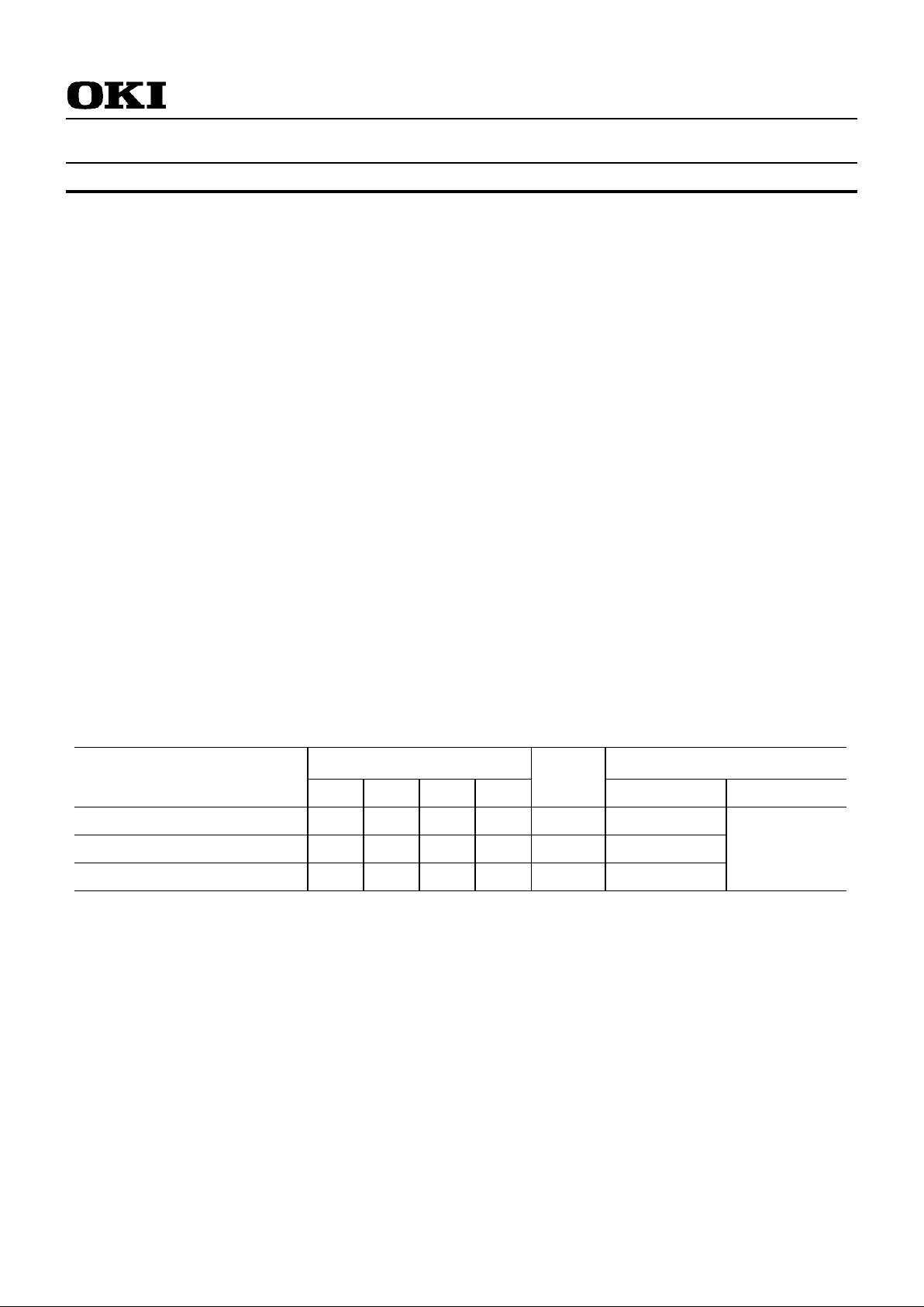
PRODUCT FAMILY
Access Time (Max. ) Power Dissipation (M ax.)
Family
t
RAC
t
AA
t
CAC
t
OEA
Cycle
Time
(Min.)
Operating Standby
MSC23V43257D-50BS8 50ns 25ns 13ns 13ns 84ns 2880mW
MSC23V43257D-60BS8 60ns 30ns 15ns 15ns 104ns 2592mW
MSC23V43257D-70BS8 70ns 35ns 20ns 20ns 124ns 2304mW
14.4mW
Page 2
Semiconductor MSC23V43257D
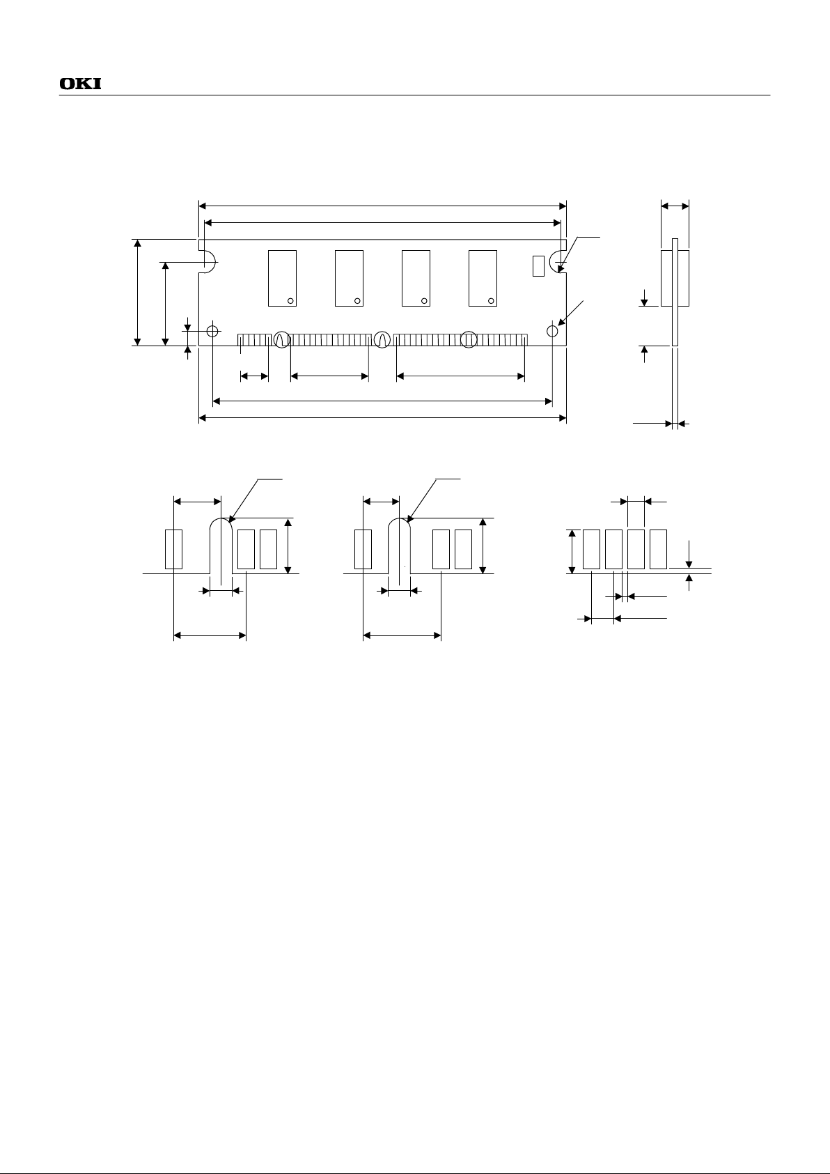
MODULE OUTLINE
1
50
R1.0
19.05±0.1
6.35±0.1
84.17 T yp.
90.19T yp.
4.0M i n.
4.00M ax.
(Uni t : mm)
MSC23V43257D-xxBS 8
2 - R2.0±0.1
2 - φ3.0±0.1
1.27±0.1
2.0±0.1
3.12±0.13
1.27±0.1
0.23M i n.
1.0±0.1
0.20
6.35±0.1
Detail A
34.29±0.1
17.80±0.13
3.0±0.13
2.0±0.1
6.35±0.1
Detail B
3.12±0.13
Detail C
A B C
25.40±0.13
4.175±0.13
3.175±0.13
88.19±0.2
90.19 ±0.2
R1.0
2.50
Page 3
Semiconductor MSC23V43257D
PIN C ONFIGURATION
Front Side Back Side Front Side Back Side
Pin No. Pin Name Pin No. Pin Name Pin No. Pin Name Pin No. Pin Name
1VSS51 V
SS
26 V
SS
76 V
SS
2DQ052DQ827NC77NC
3 DQ1 53 DQ9 28 /WE 78 /O E
4 DQ2 54 DQ10 29 /RAS0 79 NC
5 DQ3 55 DQ11 30 /RAS2 80 NC
6VCC56 V
CC
31 V
CC
81 V
CC
7 DQ4 57 DQ12 32 NC 82 NC
8 DQ5 58 DQ13 33 NC 83 NC
9 DQ6 59 DQ14 34 NC 84 NC
10 DQ7 60DQ1535 NC 85 NC
11 /CAS0 61 /CAS1 36 V
SS
86 V
SS
12 V
SS
62 V
SS
37 /CAS2 87 /CAS3
13 A0 63 A1 38 DQ16 88 DQ 24
14 A2 64 A3 39 DQ17 89 DQ 25
15 A4 65 A5 40 DQ18 90 DQ 26
16 A6 66 A7 41 DQ19 91 DQ 27
17 A8 67 A9 42 V
CC
92 V
CC
18 A10 68 NC 43DQ2093DQ28
19 NC 69 NC 44 DQ21 94 DQ29
20 NC 70 NC 45 DQ22 95 DQ30
21 V
CC
71 V
CC
46 DQ23 96 DQ31
22 NC 72 NC 47 V
SS
97 V
SS
23 NC 73 NC 48 SDA 98 SA0
24 NC 74 NC 49 SCL 99 SA1
25 NC 75 NC 50 V
CC
100 SA2
Page 4

Semiconductor MSC23V43257D
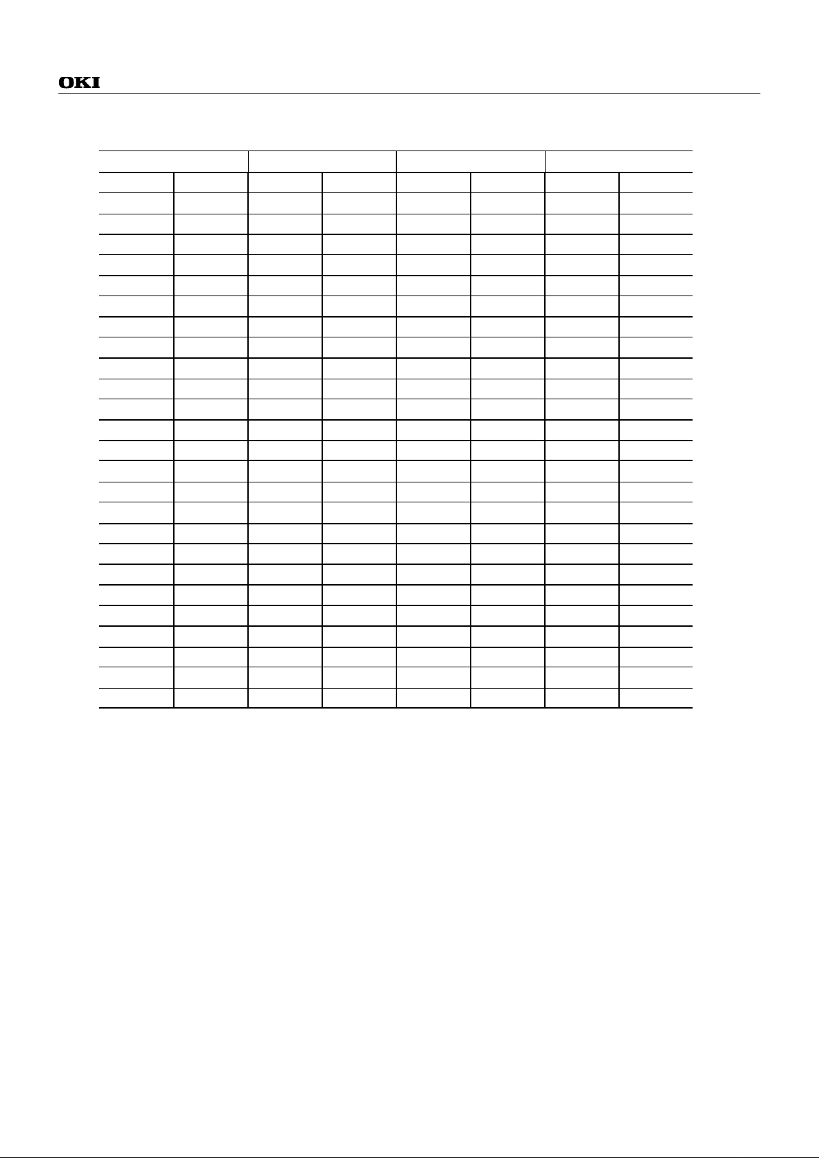
Serial PD Matrix
Byte No. Function described
SPD Value
(Hex)
Note
0 Num ber of Byt e used 80 128 Bytes
1 Total SPD Memory size 08 256 Bytes
2 Mem ory t ype 02 EDO
3 Num ber of R ows 0B 11
4 Num ber of C ol um ns 0B 11
5 Num ber of Banks 01 1
6 Module Data Width 20 32
7 Module Data Width Cont i nued 00 0
8 Suppl y Voltage 01 LVTTL
-50 32 50ns
-60 3C 60ns9
-70
/RAS Access Time
46 70ns
-50 0D 13ns
-60 0F 15ns10
-70
/CAS Access Time
14 20ns
11 D I MM Configuration type 00 Non-parity
12 Refresh Rate/Type 00 Normal Refresh
13 Primary DRAM Width 04 x4
14 Error Checking DRAM Width 00
15-61 Superset Information 00 Reserved
62 SPD Data Revision Code 01 1
-50 06
-60 1263
-70
Checksum for Byte 0-62
21
64-127 Reserved 00
128-255 Unused Storage Location (Reserved) FF
Page 5

Semiconductor MSC23V43257D
BLOCK DIAGRAM
VCCVSSC1-C8
A0-A10
A0-A10 : D0-D7
D0-D7
D0-D7
SCL
SDA
A0 A1 A2
SCL
SDA
SA0 SA1 SA 2
Serial PD
/RAS0
/WE
/OE
DQ0
DQ1
DQ2
DQ3
/CAS0
DQDQDQDQ/CAS /RAS /WE /OE
D0
DQ4
DQ5
DQ6
DQ7DQDQDQDQ
/CAS /RAS /WE /OE
D1
DQ8
DQ9
DQ10
DQ11
/CAS1
DQDQDQDQ/CAS /RAS /WE /OE
D2
DQ12
DQ13
DQ14
DQ15DQDQDQDQ
/CAS /RAS /WE /OE
D3
/RAS2
DQ16
DQ17
DQ18
DQ19
/CAS2
DQDQDQDQ/CAS /RAS /WE /OE
D4
DQ20
DQ21
DQ22
DQ23DQDQDQDQ
/CAS /RAS /WE /OE
D5
DQ24
DQ25
DQ26
DQ27
/CAS3
DQDQDQDQ/CAS /RAS /WE /OE
D6
DQ28
DQ29
DQ30
DQ31DQDQDQDQ
/CAS /RAS /WE /OE
D7
Page 6

Semiconductor MSC23V43257D
ELECTRICAL CHARACTERISTICS
Absolute Maximum Ratings
Parameter Symbol Rating Unit
Voltage on Any Pin Relative to V
SS
VIN, V
OUT
-0.5 to 4.6 V
Voltage on VCC Supply Relative t o V
SS
V
CC
-0.5 to 4.6 V
Short Ci rcui t O ut put Current I
OS
50 mA
Power Dissipation PD *8W
Operating Temperature T
OPR
0 to 70 °C
Storage Temperature T
STG
-40 to 125 °C
* Ta = 25° C
Recommended Operating Conditions
( Ta = 0°C t o 70°C )
Parameter Symbol Min. Typ. Max. Unit
V
CC
3.0 3.3 3.6 V
Power Supply Voltage
V
SS
000V
Input H i gh Voltage V
IH
2.0 - VCC+0.3 V
Input Low Voltage V
IL
-0.3 - 0.8 V
Capacitance
( V
CC
= 3.3V ±0.3V, Ta = 25°C, f = 1 MHz )
Parameter Symbol Typ. Max. Unit
Input C apaci tance (A0 – A10) C
IN1
-49pF
Input C apaci t ance (/ RAS0, /RAS2) C
IN2
-35pF
Input C apaci t ance (/ CAS0 - / CAS3) C
IN3
-20pF
Input C apaci tance (/WE) C
IN4
-65pF
I/ O C apaci tance (DQ0 - DQ31) C
I/O
-13pF
Page 7

Semiconductor MSC23V43257D
DC Characteristics
(V
CC
= 3.3V ±0.3V, Ta = 0°C to 70° C )
-50 -60 -70
Parameter Symbol Condition
Min. Max. Min. Max. Min. Max.
Unit Note
Output High Voltage V
OH
IOH = -2.0mA 2.4 V
CC
2.4 V
CC
2.4 V
CC
V
Output Low Voltage V
OL
IOL = 2.0mA 0 0. 4 0 0.4 0 0.4 V
Input Leakage Current I
LI
0V ≤ VIN ≤ VCC+0.3V;
All other pins not
under test = 0V
-80 80 -80 80 -80 80
µ
A
Output Leakage Current I
LO
DQ disable
0V ≤ V
OUT
≤ V
CC
-10 10 -10 10 -10 10
µ
A
Average Power
Supply Current
(Operating)
I
CC1
/RAS, /CAS cycling,
t
RC
= Min.
- 800 - 720 - 640 mA 1, 2
/RAS, /CAS = V
IH
-16-16-16mA
Power Supply Current
(Standby)
I
CC2
/RAS, /CAS
≥
V
CC
-0.2V
-4-4-4mA
1
Average Power
Supply Current
(/RAS only refresh)
I
CC3
/RAS cycling,
/CAS = V
IH
,
t
RC
= Min.
- 800 - 720 - 640 mA 1, 2
Average Power
Supply Current
(/CAS before /RAS refresh)
I
CC6
/RAS cycling,
/CAS before /RAS
- 800 - 720 - 640 mA 1, 2
Average Power
Supply Current
(Fast Page Mode)
I
CC7
/RAS = VIL,
/CAS cycling,
t
HPC
= Min.
- 800 - 720 - 640 mA 1, 3
Notes: 1. ICC Max. is specified as ICC for output open condition.
2. The address can be changed once or less while /RAS = V
IL
.
3. The address can be changed once or less while /CAS = V
IH
.
Page 8

Semiconductor MSC23V43257D
AC Characteristics (1/2)
(V
CC
= 3.3V ±0.3V, Ta = 0°C to 70°C ) Note: 1, 2, 3, 12, 13
-50 -60 -70
Parameter Symbol
Min. Max. Min. Max. Min. Max.
Unit Note
Random Read or Write Cycle Time t
RC
84 - 104 - 124 - ns
Read Modify Write Cycl e Time t
RWC
110 - 135 - 160 - ns
Fast Page Mode Cycle Time t
HPC
20 - 25 - 30 - ns
Fast Page Mode Read Modif y Writ e Cycle Time t
HPRWC
58 - 68 - 78 - ns
Access Time from /RAS t
RAC
-50-60-70ns4, 5, 6
Access Time from /CAS t
CAC
-13-15-20ns4, 5
Access Time from Column Address t
AA
-25-30-35ns4, 6
Access Time from /CAS Precharge t
CPA
-30-35-40ns4
Access Time from /OE t
OEA
-13-15-20ns4
Output Low Im pedance Time f rom / C AS t
CLZ
0-0-0-ns4
Data Output Hold After /CAS Low t
DOH
5-5-5-ns
/CAS to Data Output Buffer Turn-off Delay Time t
CEZ
013015020ns7, 8
/RAS to Data Output Buffer Turn-off Delay Time t
REZ
013015020ns7, 8
/OE to Data Output Buffer Turn-off Delay Time t
OEZ
013015020ns7
/WE to Data Output Buffer Turn-off Delay Time t
WEZ
013015020ns7
Transition Time t
T
150150150ns3
Refresh Period t
REF
-32-32-32ms
/RAS Precharge Time t
RP
30 - 40 - 50 - ns
/RAS Pulse Width t
RAS
50 10K 60 10K 70 10K ns
/RAS Pulse Widt h (Fast Page M ode w i t h ED O ) t
RASP
50 100K 60 100K 70 100K ns
/RAS Hold Time t
RSH
7 - 10 - 13 - ns
/RAS Hold Time referenced to /OE t
ROH
7 - 10 - 13 - ns
/CAS Precharge Time (Fast Page Mode with EDO) t
CP
7 - 10 - 10 - ns
/CAS Pulse Width t
CAS
7 10K 10 10K 13 10K ns
/CAS Hold Time t
CSH
35 - 40 - 45 - ns
/CAS to /RAS Precharge Time t
CRP
5-5-5-ns
/RAS Hold Time from /CAS Precharge t
RHCP
30 - 35 - 40 - ns
/OE Hold Time from /CAS (DQ Disable) t
CHO
5-5-5-ns
/RAS to /CAS Delay Time t
RCD
11 37 14 45 14 50 ns 5
/RAS to Column Address Delay Time t
RAD
9 2512301235 ns6
Row Address Set-up Time t
ASR
0-0-0-ns
Row Address Hold Time t
RAH
7 - 10 - 10 - ns
Column Address Set-up Time t
ASC
0-0-0-ns
Column Address Hold Time t
CAH
7 - 10 - 13 - ns
Column Address to /RAS Lead Time t
RAL
25 - 30 - 35 - ns
Page 9

Semiconductor MSC23V43257D
AC Characteristics (2/2)
(V
CC
= 3.3V ±0.3V, Ta = 0°C to 70°C ) Note: 1, 2, 3, 12, 13
-50 -60 -70
Parameter Symbol
Min. Max. Min. Max. Min. Max.
Unit Note
Read Command Set-up Time t
RCS
0-0-0-ns
Read Command Hold Time t
RCH
0-0-0-ns9
Read Command Hold Time referenced to /R AS t
RRH
0-0-0-ns9
Write Command Set-up Time t
WCS
0-0-0-ns10
Write Command Hold Time t
WCH
7 - 10 - 13 - ns
Write Command Pulse W i dt h t
WP
7 - 10 - 10 - ns
/WE Pulse Widt h (DQ D i sabl e) t
WPE
7 - 10 - 10 - ns
/OE Command Hold Time t
OEH
7 - 10 - 13 - ns
/OE Precharge Time t
OEP
7 - 10 - 10 - ns
/OE Command Hold Time t
OCH
7 - 10 - 10 - ns
Write Command to /RAS Lead Time t
RWL
7 - 10 - 13 - ns
Write Command to /CAS Lead Time t
CWL
7 - 10 - 13 - ns
Data-in Set-up Time t
DS
0-0-0-ns11
Data-in Hold Time t
DH
7 - 10 - 13 - ns 11
/OE to Data-in Delay Time t
OED
13 - 15 - 20 - ns
/CAS to /WE Delay Time t
CWD
30 - 34 - 44 - ns 10
Column Address to /WE Delay Time t
AWD
42 - 49 - 59 - ns 10
/RAS to /WE Delay Time t
RWD
67 - 79 - 94 - ns 10
/CAS Precharge /WE Delay Time t
CPWD
47 - 54 - 64 - ns 10
/CAS Active Delay Time from /RAS Precharge t
RPC
5-5-5-ns
/RAS to /CAS Set-up Time (/CAS before /RAS) t
CSR
5-5-5-ns
/RAS to /CAS Hold Time (/CAS before /RAS) t
CHR
10 - 10 - 10 - ns
/WE to /RAS Precharge Time (/CAS before /RAS) t
WRP
10 - 10 - 10 - ns
/WE Hold Time from /RAS (/CAS before /RAS) t
WRH
10 - 10 - 10 - ns
/RAS to /WE Set-up Time (Test Mode) t
WTS
10 - 10 - 10 - ns
/RAS to /WE Hold Time (Test Mode) t
WTH
10 - 10 - 10 - ns
Page 10

Semiconductor MSC23V43257D
Notes: 1. A start-up delay of 200µs is required after power-up, followed by a minimum of eight initializati on cycles
(/RAS only r efresh or /CAS before /RAS ref r esh) before proper device operation is achiev ed.
2. The AC characteristics assume t
T
= 2ns.
3. V
IH
(Min.) and VIL(Max.) are reference level s for measuring input ti ming signals. Transition times (tT) are
measured between V
IH
and VIL.
4. This paramet er is measured with a load ci r c uit equivalent to 1 TTL load and 100pF.
The output timing reference levels are V
OH
= 2.0V and V
OL
= 0.8V.
5. Operation wit hin the t
RCD
(Max.) limi t ensures that t
RAC
(Max.) can be met.
t
RCD
(Max.) is specified as a reference point only. If t
RCD
is greater than the specified t
RCD
(Max.) limit, then
the access tim e is controlled by t
CAC
.
6. Operation wit hin the t
RAD
(Max.) limi t ensures that t
RAC
(Max.) can be met.
t
RAD
(Max.) is specified as a reference point only. If t
RAD
is greater than the specified t
RAD
(Max.) limit, then
the access tim e is controlled by t
AA
.
7. t
CEZ
(Max.), t
REZ
(Max.), t
WEZ
(Max.) and t
OEZ
(Max.) def i ne the ti m e at which the out put achieves the open
circui t condition and are not referenced to output voltage levels.
8. t
CEZ
or t
REZ
must be satisfied for open circuit condition.
9. t
RCH
or t
RRH
must be satisfi ed for a read cycle.
10. t
WCS
, t
CWD
, t
RWD
, t
AWD
and t
CPWD
are not restricti v e operati ng parameter s. They are incl uded in the data
sheet as electric al characteristics only. If t
WCS ≥ tWCS
(Min.), then t he cycle is an early write cycle and the
data out will remain open circuit (high i mpedance) throughout the enti r e cycle. If t
CWD
≥ t
CWD
(Min.), t
RWD
≥ t
RWD
(Min.), t
AWD
≥ t
AWD
(Min.) and t
CPWD
≥ t
CPWD
(Min.), then the cycl e is a read modif y write cycle and
data ou t w ill c on ta in d a ta r ead from the selected cell; if neither of the above sets of conditions is satisfied,
then the condition of the data out (at access time) is indeterminate.
11. These parameters are referenced to the /CAS leading edge in an early write cycle, and to the /WE
leading edge in an /OE control write cycle, or a read modify write cycle.
12. The test mode is initiated by performing a /WE and /CAS before /RAS ref resh cycle. This mode is
latched and remains in effect until the exit cycle is generated. The test mode specified in this data sheet
is an 8-bit parallel test functi on. CA0, CA1 and CA10 are not used. In a read cycle, if all internal bits are
equal, the DQ pin will indic ate a hig h le vel. If an y in te rn al b its a re no t equal, the DQ pin will indica te a lo w
levels. The test mode is cleared and the memory device returned to its normal operating state by
performing a /RAS only refresh cycle or a /CAS before /RAS refresh cycle.
13. In a test mode read cycle, the value of access time parameters is delayed for 5ns for the specified value.
These parameters should be specifi ed in test m ode cycle by adding the abov e v alue t o the specif ied
value in this data sheet.
 Loading...