

Page 1
MSC23S4721E-8BS18 (98.07.17)
Semiconductor
MSC23S4721E-8BS18
4,194,304 Word x 72 Bit SYNCHRONOUS DYNAMIC RAM MODULE (2BANK):
DESCRIPTION
The Oki MSC23S4721E-8BS18 is a fully decoded, 4,194,304 x 72bit synchronous
dynamic random access memory composed of eighteen 16Mb DRAMs (2Mx8) in TSOP
packages mounted with decoupling capacitors on a 168-pin glass epoxy Dual-in-Line
Package supports any application where high density and large capacity of storage
memory are required, like for example PCs or servers.
FEATURES
• 4-Meg Word x 72-Bit (2Bank 8 Byte) organization
• 168-pin Dual Inline Memory Module
• All DQ Pins have 10Ω Damping Resister
• Single 3.3V power supply, ±0.3V tolerance
• Input :LVTTL compatible
• Output :LVTTL compatible
• Refresh : 4,096 cycles/64 ms
• Programmable data transfer mode
• /CAS latency (2, 3)
• Burst length (1, 2, 4, 8, Full)
• Data scramble(sequential, interleave)
• CBR auto-refresh, Self-refresh capability
• Serial Presence Detect (SPD) With EEPROM
PRODUCT ORGA NIZATION
Product Nam e Operation Access Time (Max.)
Frequency (Max.) t
MSC23S4721E -8BS18 125MHz 10.0ns 6.0ns
Note. Specification are subject to chan ge with out n otice.
AC2
t
AC3
Page 1/11
Page 2

MSC23S4721E-8BS18 (98.07.17)
/
/
/
/
/
/
/
/
/
/
/
/
/
/
/
/
/
/
/
/
Ω
/
/
/
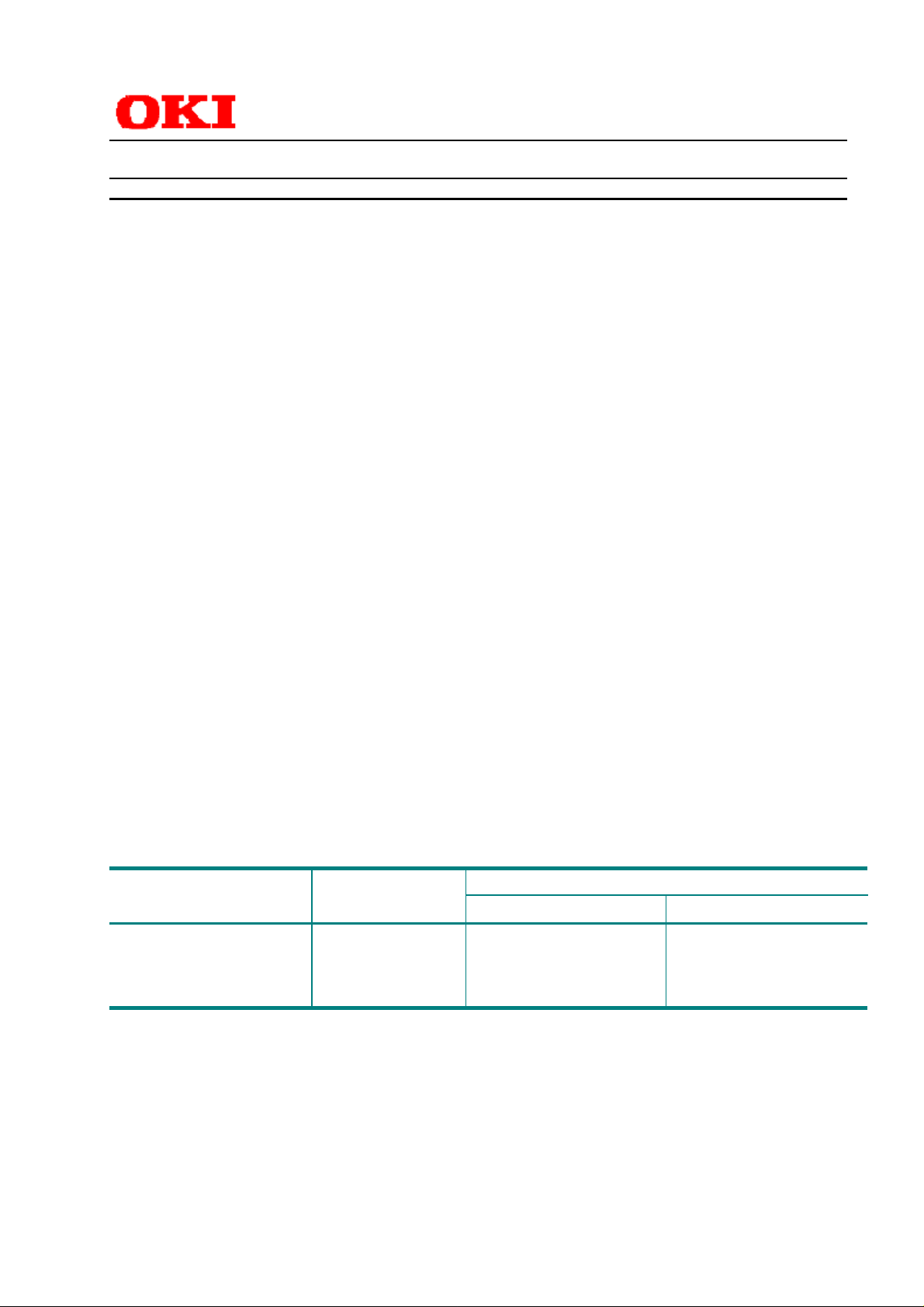
BLOCK DIAGRAM
CKE1
CKE0
CS0
DQMB0
DQ0
DQ7
DQMB1
DQ8
DQ15
DQMB4
DQ32
DQ39
DQMB5
DQ40
DQ47
DQM CKE
DQ0
CS
1
DQ7
DQM CKE
DQ0
CS
2
DQ7
DQM CKE
DQ0
CS
3
DQ7
DQM CKE
DQ0
CS
4
DQ7
CS1
DQM CKE
DQ0
DQ7
DQM CKE
DQ0
DQ7
DQM CKE
DQ0
DQ7
DQM CKE
DQ0
DQ7
CS
10 15
CS
11
CS
12
CS
13
CS2
DQMB2
DQ16
DQ23
DQMB3
DQ24
DQ31
DQMB6
DQ48
DQ55
DQMB7
DQ56
DQ63
DQM CKE
DQ0
CS
6
DQ7
DQM CKE
DQ0
CS
7
DQ7
DQM CKE
DQ0
CS
8
DQ7
DQM CKE
DQ0
CS
9
DQ7
CS3
DQM CKE
DQ0
DQ7
DQM CKE
DQ0
DQ7
DQM CKE
DQ0
DQ7
DQM CKE
DQ0
DQ7
CS
CS
16
CS
17
CS
18
10K
DQMB1
CB0
CB7
CLK0
RAS,/CAS,/WE
A0-A11
DQM CKE
DQ0
CS
5
DQ7
1
2
3
4
5
DQMB5
DQM CKE
DQ0
DQ7
CLK1
118
á
CS
14
10
11
12
13
14
Vcc
Vss
Note. The Value of all resistors is 10Ω expect WP and CKE1
MODULE OUTLINE
SCL
CLK2
0.1uF 0.33uF
Serial PD
A0 A1 A2
SA0 SA1 SA2
3.3pF
19
47K
Ω
SDA
WP
15
716
8
CLK3
9
Two Decoupling Capacitors
per SDRAM
3.3pF
17
18
(Front)
(Back)
109411
1
85
95
40
12441125
84
168
Page 2/11
Page 3
MSC23S4721E-8BS18 (98.07.17)
de
de
de
de
)
)
)
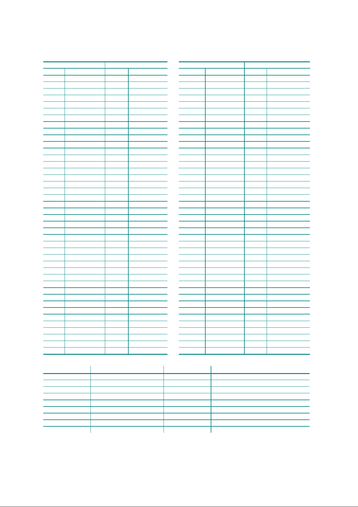
PIN CONFIGURATION
Front si
Pin No. Pin name Pin No. Pin name Pin No. Pin name Pin No. Pin name
1 VSS 85 VSS 43 VSS 127 VSS
2 DQ0 86 DQ32 44 N.C 128 CKE0
3 DQ1 87 DQ33 45 /CS2 129 /CS3
4 DQ2 88 DQ34 46 DQMB2 130 DQMB6
5 DQ3 89 DQ35 47 DQMB3 131 DQMB7
6 VCC 90 VCC 48 N.C 132 N.C
7 DQ4 91 DQ36 49 VCC 133 VCC
8 DQ5 92 DQ37 50 N.C 134 N.C
9 DQ6 93 DQ38 51 N.C 135 N.C
10 DQ7 94 DQ39 52 CB2 136 CB6
11 DQ8 95 DQ40 53 CB3 137 CB7
12 VSS 96 VSS 54 VSS 138 VSS
13 DQ9 97 DQ41 55 DQ16 139 DQ48
14 DQ10 98 DQ42 56 DQ17 140 DQ49
15 DQ11 99 DQ43 57 DQ18 141 DQ50
16 DQ12 100 DQ44 58 DQ19 142 DQ51
17 DQ13 101 DQ45 59 VCC 143 VCC
18 VCC 102 VCC 60 DQ20 144 DQ52
19 DQ14 103 DQ46 61 N.C 145 N.C
20 DQ15 104 DQ47 62 N.C 146 N.C
21 CB0 105 CB4 63 CKE1 147 N.C
22 CB1 106 CB5 64 VSS 148 VSS
23 VSS 107 VSS 65 DQ21 149 DQ53
24 N.C 108 N.C 66 DQ22 150 DQ54
25 N.C 109 N.C 67 DQ23 151 DQ55
26 VCC 110 VCC 68 VSS 152 VSS
27 /WE 111 /CAS 69 DQ24 153 DQ56
28 DQMB0 112 DQMB4 70 DQ25 154 DQ57
29 DQMB1 113 DQMB5 71 DQ26 155 DQ58
30 /CS0 114 /CS1 72 DQ27 156 DQ59
31 N.C 115 /RAS 73 VCC 157 VCC
32 VSS 116 VSS 74 DQ28 158 DQ60
33 A0 117 A1 75 DQ29 159 DQ61
34 A2 118 A3 76 DQ30 160 DQ62
35 A4 119 A5 77 DQ31 161 DQ63
36 A6 120 A7 78 VSS 162 VSS
37 A8 121 A9 79 CLK2 163 CLK3
38 A10 122 A11(BA0
39 N.C 123 N.C 81 WP 165 SA0
40 VCC 124 VCC 82 SDA 166 SA1
41 VCC 125 CLK1 83 SCL 167 SA2
42 CLK0 126 N.C 84 VCC 168 VCC
Back si
Front si
80 N.C 164 N.C
Back si
Pin Name Function Pin Name Function
VCC Power Supply (3.3V
VSS Ground (0V
CLK# System Clock DQ#, CB# Data Input/Output
/CS# Chip Select WP Write Protect
CKE# Clock E nable SDA Data I/O for SPD
A0-A10 Address SCL CLK input f or S P D
A11 Bank Select Address SA# Socket Position Address for SPD
/RAS Row Address Strobe N.C No Connection
/CAS Colum n A ddr ess Strobe
/WE Wri te Enable
DQMB# Data Input/Output Mask
Page 3/11
Page 4

MSC23S4721E-8BS18 (98.07.17)
,38,42,53,31,38,20,20,
SERIAL PRESENCE DET ECT
Byte
No.
0
1
2
3
4
5
6
7
8
9
10
11
12
13
14
15
16
17
18
19
20
21
22
23
24
25
26
27
28
29
30
31
32
33
34
35
36-61
62
63
64-71
72
73-90
91, 92
93-125
126
127
128-255
41,45,20,20,20,20,20,20 Manufacturer’s JEDEC ID code
43,32,33,53,34,37,32,31,45,
2D
SPD
Remark Notes
Hex Value
80
Defines the number of by tes written int o
128 byte
SPD memory
08 Total number of by tes of SPD memory 256 byte
04 Fundamental memory type SDRAM
0B Number of rows 11 rows
09 Number of colum ns 9 columns
02 Number of module bank s 2 bank
48 Data width of this assembly 72 bits
00 ... Data width continuation 0
01 Voltage i nterface lev el LVTTL
80 Cycle time (CL=3) CL=3 tCC=8ns
60 Access time from CLK (CL=3) CL=3 t
02 DIMM configuration type Non Parity
80 Refresh rate / type Normal / Self
08 Primary SDRAM width x8
08 Error checking SDRAM width
01 Minimum CLK delay t
CCD
: 1 CLK
8F Burst lengths supported 1, 2, 4, 8, F
02 Number of banks on each SDRAM 2 banks
06 /CAS lat enc y 2, 3
01 /CS latenc y 0
01 /WE latency 0
00 SDRAM module attri butes
06 SDRAM device att r ibutes : General
C0 Cycle time (CL=2) CL=2 t
A0 Access time from CLK (CL=2) CL=2 t
00 Cycle time (CL=1) Not support
00 Access time fr om CLK (CL=1) Not support
14 Minimum ROW prec har ge time tRP=20ns
14 /RAS to /RA S bank delay t
14 /RAS to /CAS delay t
30 Minimum /RA S pulse width t
RRD
RCD
RAS
=20ns
=20ns
=48ns
04 Density of eac h bank on module 16MB
20
10
Command and addr ess signal input setup time
Command and addr ess signal input hold time
2ns
1ns
20 Data signal i nput setup time 2ns
10 Data signal i nput hold ti me 1ns
00-00 R.F.U
12 SPD data revision code 1.2
3F Chec k sum for byte 0-62
01 / 06 Manufacturing location
Manufact ur er ’s part number C23S 4721E - 8B S 18
20
20, 20 Revision code
00-00 R.F.U
64 Intel speci fication f r equenc y 100MHz
F5 Intel specification /CAS latency CLK0-3, CL=3
FF-FF Unused storage l oc ations
AC3
CC2
AC2
=6ns
=12ns
=10ns
Page 4/11
Page 5

MSC23S4721E-8BS18 (98.07.17)
ELECTRICAL CHARACTERISTICS
Absolute Maximum Ratings
Rating Symbol Value Unit
Voltage on any pin relative to Vss VIN, V
Vcc supply volt age Vcc, VccQ -0.5 to 4.6 V
Storage temperature T
Power dissipation P
Short circuit current I
Operating temperatur e T
stg
D
os
opr
OUT
*
-0.5 to VCC+0.5 V
- 55 to 125 °C
18 W
50 mA
0 to 70 °C
*: Ta=25
°C
Recommended Operating Conditions
Parameter Symbol Min. Typ. M ax. Unit
Power supply voltage Vcc, VccQ 3.0 3.3 3.6 V
Input high voltage V
Input low voltage V
IH
IL
2.0 - VCC+0.3 V
-0.3 - 0.8 V
(Voltages referenced to Vss = 0V)
Capacitance
Parameter Symbol Max. Un it
Input capaci tance(A0-A11, /RAS, /CAS , /WE) C
Input capaci tance(/CS0, /CS1, /CS2, /CS3) C
Input capaci tance(DQMB0-DQMB7) C
Input capaci tance(CKE0, CKE 1) C
I/O capacitance(DQ 0- DQ63, CB0- CB7) C
Input capaci tance(CLK0, CLK1, CLK 2, CLK3) C
(Vcc=3.3V ± 0.3V, Ta=25°C f=1MHz)
IN1
IN2
IN3
IN4
I/O
CLK
104 pF
34 pF
22 pF
58 pF
25 pF
50 pF
Page 5/11
Page 6

MSC23S4721E-8BS18 (98.07.17)
DC CHARACTERISTICS
Parameter Symbol
Input Leakage
Current
Bank CKE Ot hers Min Max
I
LI
- -
Condition
(VCC = 3.3V ± 0.3V, Ta = 0 to 70°C)
Module
Spec.
-
-180 180
Unit
uA
Note
Output Leakage
Current
Output High
Voltage
Output Low
Voltage
Average Power
Supply Current
(Operating)
Power Supply
Current
(Stand by)
Average Power
Supply Current
(Clock
Suspenson)
Average Power
Supply Current
(Active Stand by)
Power Supply
Current (Burst)
Power Supply
Current
(Auto-Refresh)
I
LO
V
OH
V
OL
ICC1
ICC1D
ICC2
ICC3S
ICC3
ICC4
ICC5
--
--
--
One Bank
Activ e
CKE ≥ V
Both
Banks
CKE ≥ V
Activ e
Both
Banks
CKE ≥ V
Precharge
Both
Banks
CKE ≤ V
Activ e
One
Banks
CKE ≥ V
Activ e
Both
Banks
CKE ≥ V
Activ e
One Bank
Activ e
CKE ≥ V
I
OH
I
OL
tCC=min.
t
IH
No Burst
tCC=min.
t
IH
t
RRD
No Burst
tCC=min.
IH
tCC=min.
IL
tCC=min.
IH
tCC=min.
IH
tCC=min.
IH
t
-
= -2mA 2.4
-20
20
-
= 2mA - 0.4 V
=min
RC
RC
=min
=min
- 1125 mA 1, 2
- 1395 mA 1, 2
- 720 mA 3
- 387 mA 2
- 765 mA 3
- 1305 mA 1, 2
RC
=min
- 1080 mA 2
uA
V
Average Power
Supply Current
(Self-Refresh)
Average Power
Supply Current
(Power down)
ICC6
ICC7
Both
Banks
Precharge
Both
Banks
Precharge
NOTE: 1. Meas ur ed with the output open.
2. The address and data can be changed once or left uncharged during one cycle.
3. The address and data can be changed once or left unchanged during two cycles.
CKE ≤ V
CKE ≤ V
IL
IL
tCC=min.
tCC=min.
-36mA
-36mA
Page 6/11
Page 7

MSC23S4721E-8BS18 (98.07.17)
y
MODE SET ADDRESS KEYS
/CAS Latenc
A6 A5 A4 CL A3 BT A2 A1 A0 BT= 0 BT= 1
0 0 0 Reserved 0 Sequential 0 0 0 1 1
0 0 1 Reserved 1 Interleave 0 0 1 2 2
0102 0104 4
0113 0118 8
1 0 0 Reserved 1 0 0 Reserved Reserved
1 0 1 Reserved 1 0 1 Reserved Reserved
1 1 0 Reserved 1 1 0 Reserved Reserved
1 1 1 Reserved 1 1 1 Full P age Reserved
Note: A7, A8, A9, A10 and A11 should stay "L" during mode set cycle.
Burst Type Burst Length
POW ER ON SEQUE NCE
1. With inputs in NOP state, turn on the power supply and start the system clock.
2. After the VCC voltage has reached the specified level, pause for 200us or more
with the input kept in NOP state.
3. Issue the precharge all bank command.
4. Apply a CBR auto-refresh eight or more times.
5. Enter the mode register setting command.
Page 7/11
Page 8

MSC23S4721E-8BS18 (98.07.17)
AC CHARACTERISTI C
NOTE 1, 2 .
Parameter Symbol Module Spec. Unit Note
Clock Cycle Time CL=3 t
CL=2 12 - ns
Access Time from Clock CL=3 t
CL=2 - 10 ns 3, 4
Clock "H" Pulse Time t
Clock "L" Pulse Time t
Input Setup T ime(CLK, ADD, DIN) t
Input Hold T ime(CLK, ADD, DIN) t
Output Low Im pedanc e Time from Clock t
Output Hi gh Impedance Time from Clock t
Output Hol d from Clock t
/RAS Cycle Time t
/RAS Precharge Time t
/RAS Activ e Time t
/RAS to /CAS Delay Time t
Wr ite Recovery Time t
Wr ite Command Input T ime from O utput t
/RAS to /RAS Bank Active Delay Time t
Refresh Ti me t
Power-down Exit Set-up Time t
Input Level Transi tion Ti me t
/CAS to /CAS Delay Time (Min) I
Clock Disabl e Time from CK E I
Data Output High Impedanc e Time from DQM I
Data Input Mask Time from DQ M B I
Data Input Time from Write Command I
Data Output High Inpedance Time I
Active Com mand Input T ime from MODE I
NOTES:
1) AC measurem ents assume that t
=1ns.
T
2) The r eference level for t im ing of input signals is 1.4V.
3) T his par am eter is measured with a load c ir c uit equivalent to 1 TTL load and 50pF
(R
is 50ohm).
Load
4) An acc es s time is measured at 1.4V.
5) If t
is longer than 1ns, t he r eference level for t im ing of input signals are V
T
CC
AC
CH
CL
SI
HI
OLZ
OHZ
OH
RC
RP
RAS
RCD
WR
OWD
RRD
REF
PDE
T
CCD
CKE
DOZ
DOD
DWD
ROH
MRD
(VCC = 3.3 ± 0. 3V , Ta = 0 ~70°C)
Min. Max.
8-ns
- 6 ns 3, 4
3-ns
3-ns
2-ns
1-ns
3-ns
-9ns
3-ns
70 - ns
20 - ns
48 100,000 ns
20 - ns
8-ns
20 - ns
20 - ns
-64ms
10 - ns
-3ns
1 Cycle
1 Cycle
2 Cycle
0 Cycle
0 Cycle
CL Cycle
3 Cycle
and V
IH
IL.
OUTPUT
OUTPUT LOAD
1.4v
50
50pF
Page 8/11
Ω
Page 9

MSC23S4721E-8BS18 (98.07.17)
FUNCTION TRUTH TABL E (Table1)(1/2)
Current State /CS /RAS /CAS /WE BA ADDR Action
Idle H X X X X X NOP
LHHHXXNOP
L H H L BA X ILLEGAL
L H L X BA CA ILLEGAL
L L H H BA RA Row Active
L L H L BA A10 NOP
L L L H X X Auto-Refresh or Self-Refresh
L L L L L OP Code Mode Register write
Row Active H X X X X X NOP
LHHXXXNOP
L H L H BA CA, A10 Read
L H L L BA CA, A10 Write
L L H H BA RA ILLEGAL
L L H L BA A10 Precharge
LLLXXXILLEGAL
Read H X X X X X NOP (Continue Row Active after Burst ends)
L H H H X X NOP (Continue Row Active after Burst ends)
L H H L BA X Reserved
L H L H BA CA, A1 0 Term Bu rst, s ta rt n ew Burst Read
L H L L BA CA, A1 0 Te rm Bu rs t, sta rt n ew Burst Write
L L H H BA RA ILLEGAL
L L H L BA A10 Term Burst, execute Row Precharge
LLLXXXILLEGAL
Write H X X X X X
LHHHXX
NOP (Continue Row Active after Burst ends)
NOP (Continue Row Active after Burst ends)
L H H L BA X ILLEGAL
L H L H BA CA, A1 0 Term Bu rst, s ta rt n ew Burst Read
L H L L BA CA, A1 0 Te rm Bu rs t, sta rt n ew Burst Write
L L H H BA RA ILLEGAL
L L H L BA A10 Term Burst, execute Row Precharge
LLLXXXILLEGAL
Read with H X X X X X
Auto Precharge L H H H X X
NOP (Continue Burst to End and ente r Row Pre charge )
NOP (Continue Burst to End and ente r Row Pre charge )
L H H L BA X ILLEGAL
L H L H BA CA, A10 ILLEGAL
L H L L X X ILLEGAL
L L H X BA RA, A10 ILLEGAL
LLLXXXILLEGAL
Wri te with H X X X X X
Auto Precharge L H H H X X
NOP (Continue Burst to End and ente r Row Pre charge )
NOP (Continue Burst to End and ente r Row Pre charge )
L H H L BA X ILLEGAL
L H L H BA CA, A10 ILLEGAL
L H L L X X ILLEGAL
L L H X BA RA, A10 ILLEGAL
LLLXXXILLEGAL
2
2
4
5
2
2
2
2
2
2
2
2
2
2
Page 9/11
Page 10

MSC23S4721E-8BS18 (98.07.17)
FUNCTION TRUTH TABL E (Table1)(2/2)
Current State /CS /RAS /CAS /WE BA ADDR Action
Æ
Precharge H X X X X X NOP
LHHHXXNOP
L H H L BA X ILLEGAL
L H L X BA CA ILLEGAL
L L H H BA RA ILLEGAL
L L H L BA A10 NOP
LLLXXXILLEGAL
Write H X X X X X NOP
Recovery L H H H X X NOP
L H H L BA X ILLEGAL
L H L X BA CA ILLEGAL
L L H H BA RA ILLEGAL
L L H L BA A10 ILLEGAL
LLLXXXILLEGAL
Row Active H X X X X X NOP Row Active after t
L H H H X X NOP Row Active after t
L H H L BA X ILLEGAL
L H L X BA CA ILLEGAL
L L H H BA RA ILLEGAL
L L H L BA A10 ILLEGAL
LLLXXXILLEGAL
Refresh H X X X X X NOP Æ Idle after t
LHHXXXNOP
L H L X X X ILLEGAL
L L H X X X ILLEGAL
LLLXXXILLEGAL
Mode Re sister H X X X X X NOP
Access L H H H X X NOP
L H H L X X ILLEGAL
L H L X X X ILLEGAL
L L X X X X ILLEGAL
Idle after t
Æ
Idle after t
2
2
2
4
2
2
2
2
2
2
2
2
Æ
Idle after t
RP
RP
RCD
RCD
RC
RC
ABBREVIATIONS
RA = Row Addres s BA = Bank Address NOP = No Operation c omm and
CA = Column Address AP = Auto Precharge
Notes:
1.
All inputs will be enabled when CKE i s set hi gh for at least 1 cycl e pri or to the inputs.
2.
Illegal to bank i n spec ified st ate, but may be l egal i n som e c ases dependi ng on the s tate of
bank selection.
3.
Satisfy the timing of t
4.
NOP to bank prechar ging or i n idl e s tate. Pr echar ges ac ti vated bank by BA or A10.
5.
Illegal if any bank i s not i dl e.
and tWR to prevent bus contention.
CCD
Page 10/11
Page 11

MSC23S4721E-8BS18 (98.07.17)
FUNCTION TRUTH TABL E (CKE) (Table2)
Current State (n) CKEn-1 CKEn /CS /RAS /CAS /WE ADDR Action
Self R efresh H X X X X X X INVALID
L H H X X X X Exit Self Refresh Æ ABI
L H L H H H X Exit Self Refresh Æ ABI
L H L H H L X ILLEGAL
L H L H L X X ILLEGAL
L H L L X X X ILLEGAL
L L X X X X X NOP (Maintain Self Refresh)
H X X X X X X INVALID
Power Down L H H X X X X Exit Power Down Æ ABI
L H L H H H X Exit Power Down Æ ABI
L H L H H L X ILLEGAL
L H L H L X X ILLEGAL
L H L L X X X ILLEGAL
All Ban k s idle
(ABI) H L H X X X X Enter Power Down
Any State H H X X X X X Refer to Operations in Table 1
Other than H L X X X X X Begin Clock Suspend Next Cycle
Listed Above L H X X X X X Enable Clock of Next Cycle
6
L L X X X X X NOP (Continue power down mode)
H H X X X X X Refer to Table 1
H L L H H H X Enter Power Down
H L L H H L X ILLEGAL
H L L H L X X ILLEGAL
H L L L H L X ILLEGAL
H L L L L H X Enter Self Re fresh
H L L L L L X ILLEGAL
LLXXXXXNOP
L L X X X X X Continue Clock Suspension
6
Notes:
6.
Power-down and s el f refresh can be enter ed onl y when al l the bank s ar e i n an i dle s tate.
Page 11/11
 Loading...