March 2010
BS170 / MMBF170
N-Channel Enhancement Mode Field Effect Transistor
BS170 / MMBF170 — N-Channel Enhancement Mode Field Effect Transistor
General Description
These N-Channel enhancement mode field ef fec t
transistors are produced using Fairchild's proprietary, high
cell density, DMOS technology. These products have been
designed to minimize on-state resistance while provide
rugged, reliable, and fast switching performance. They can
be used in most applications requiring up to 500mA DC.
Features
■ High density cell design for low R
■ Voltage controlled small signal switch.
■ Rugged and reliable.
■ High saturation current capability.
These products are particularly sui ted for low vol tage, low
current applications such as small servo motor control,
power MOSFET gate drivers, and other switching
applications.
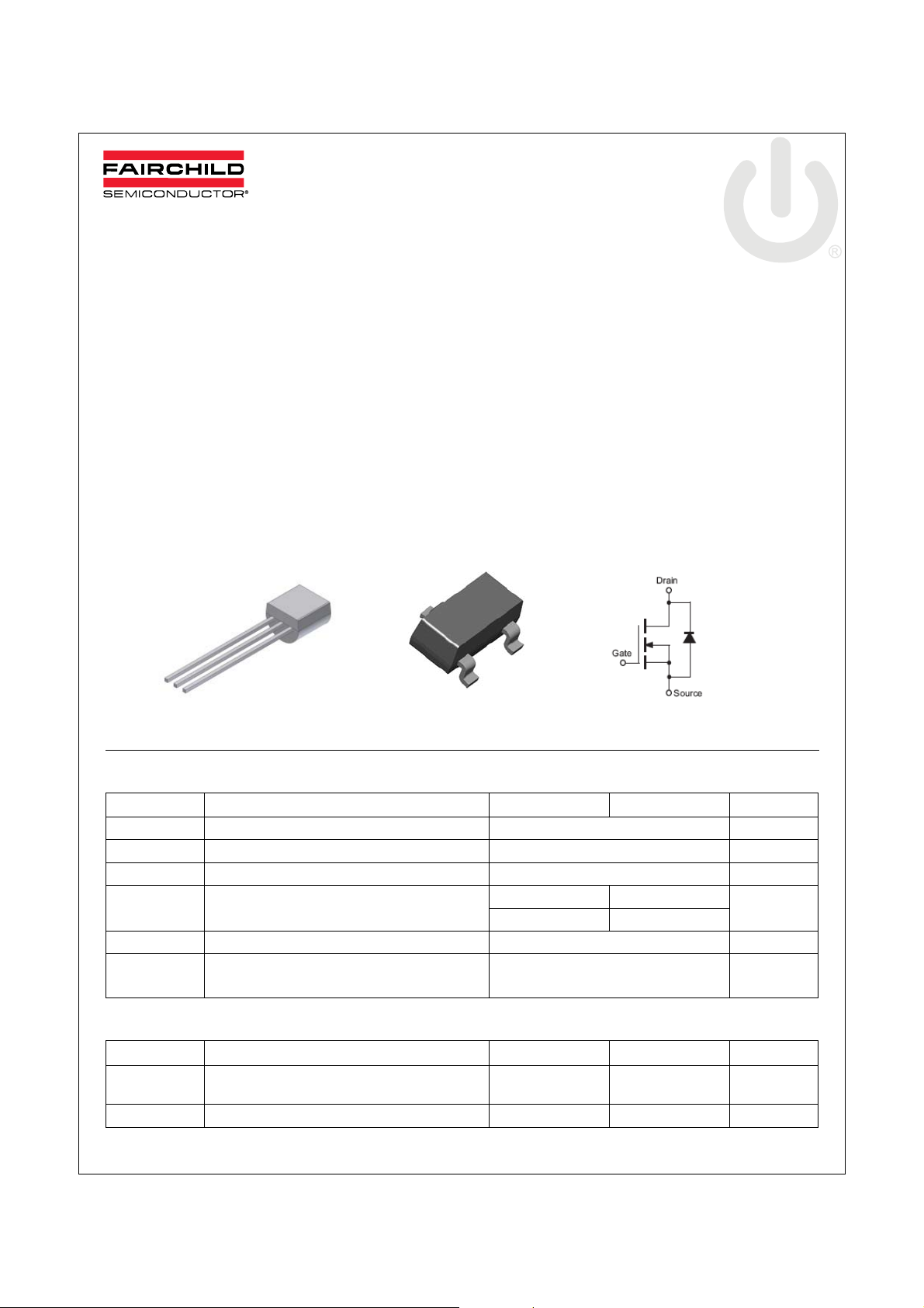
BS170 MMBF170
D
S
D
G
S
TO-92
G
SOT-23
DS(ON)
.
Absolute Maximum Ratings T
= 25°C unless otherwise noted
A
Symbol Parameter BS170 MMBF170 Units
V
DSS
V
DGR
V
GSS
I
D
T
, T
J
STG
T
L
Thermal Characteristics T
Drain-Source Voltage 60 V
Drain-Gate Voltage (R
≤ 1MΩ)60V
GS
Gate-Source V oltage ± 20 V
Drain Current - Continuous 500 500
- Pulsed 1200 800
mA
Operating and Storage Temperature Range - 55 to 150 °C
Maximum Lead Temperature for Soldering
300 °C
Purposes, 1/16" from Case for 10 Seconds
= 25°C unless otherwi s e noted
A
Symbol Parameter BS170 MMBF170 Units
P
D
R
θJA
© 2010 Fairchild Semiconductor Corporation www.fairchildsemi.com
BS170 / MMBF170 Rev. E2 1
Maximum Power Dissipation
Derate above 25°C
830
6.6
300
2.4
mW
mW/°C
Thermal Resistance, Junction to Ambient 150 417 °C/W

BS170 / MMBF170 — N-Channel Enhancement Mode Field Effect Transistor
Electrical Characteristics T
=25°C unless otherwise noted
A
Symbol Parameter Conditions Type Min. Typ. Max. Units
OFF CHARACTERISTICS
BV
I
DSS
I
GSSF
ON CHARACTERISTICS (Notes 1)
V
GS(th)
R
DS(ON)
g
Dynamic Characteristics
C
C
C
Switching Characteristics (Notes 1)
Drain-Source Breakdown Voltage VGS = 0V, ID = 100μAAll60 V
DSS
Zero Gate Voltage Drain Current VDS = 25V, VGS = 0V All 0.5 μA
Gate - Body Leakage, Forward VGS = 15V, VDS = 0V All 10 nA
Gate Threshold Voltage VDS = VGS, ID = 1mA All 0.8 2.1 3 V
Static Drain-Source On-Resistance VGS = 10V, ID = 200mA All 1.2 5 Ω
Forward Transconductance VDS = 10V, ID = 200mA BS170 320 mS
FS
≥ 2 V
V
DS
= 200mA
I
D
Input Capacitance VDS = 10V, VGS = 0V,
iss
Output Capacitance All 17 30 pF
oss
Reverse Transfer Capacitance All 7 10 pF
rss
Turn-On Time VDD = 25V, ID = 200mA,
t
on
Turn-Off Time VDD = 25V, ID = 200mA,
t
off
f = 1.0MHz
= 10V, R
V
GS
= 25V, ID = 500mA,
V
DD
= 10V, R
V
GS
= 10V, R
V
GS
= 25V, ID = 500mA,
V
DD
= 10V, R
V
GS
DS(on)
GEN
GEN
GEN
GEN
,
= 25Ω
= 50Ω
= 25Ω
= 50Ω
MMBF170 320
All 24 40 pF
BS170 10 ns
MMBF170 10
BS170 10 ns
MMBF170 10
Note:
1. Pulse Test: Pulse Width ≤ 300μs, Duty Cycle ≤ 2.0%.
Ordering Information
Part Number Package Package Type Lead Frame Pin array
BS170 TO-92 BULK STRAIGHT D G S
BS170_D26Z TO-92 Tape and Reel FORMING D G S
BS170_D27Z TO-92 Tape and Reel FORMING D G S
BS170_D74Z TO-92 AMMO FORMING D G S
BS170_D75Z TO-92 AMMO FORMING D G S
MMBF170 SOT-23 Tape and Reel
© 2010 Fairchild Semiconductor Corporation www.fairchildsemi.com
BS170 / MMBF170 Rev. E2 2

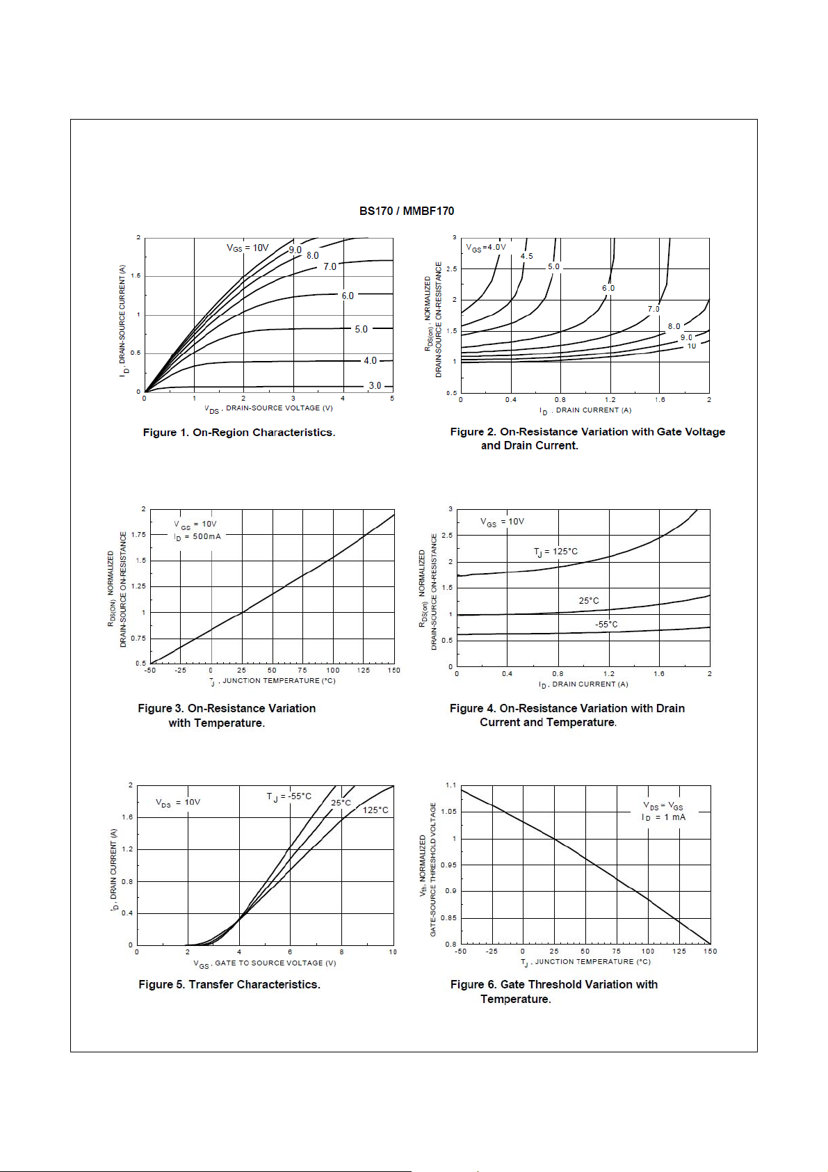
Typical Electrical Characteristics
BS170 / MMBF170 — N-Channel Enhancement Mode Field Effect Transistor
© 2010 Fairchild Semiconductor Corporation www.fairchildsemi.com
BS170 / MMBF170 Rev. E2 3

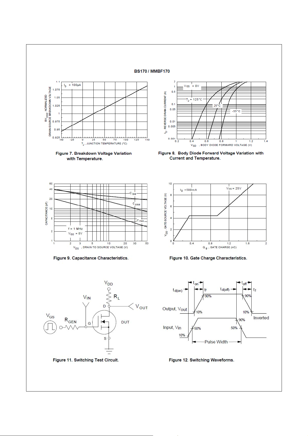
Typical Electrical Characteristics (continued)
BS170 / MMBF170 — N-Channel Enhancement Mode Field Effect Transistor
© 2010 Fairchild Semiconductor Corporation www.fairchildsemi.com
BS170 / MMBF170 Rev. E2 4

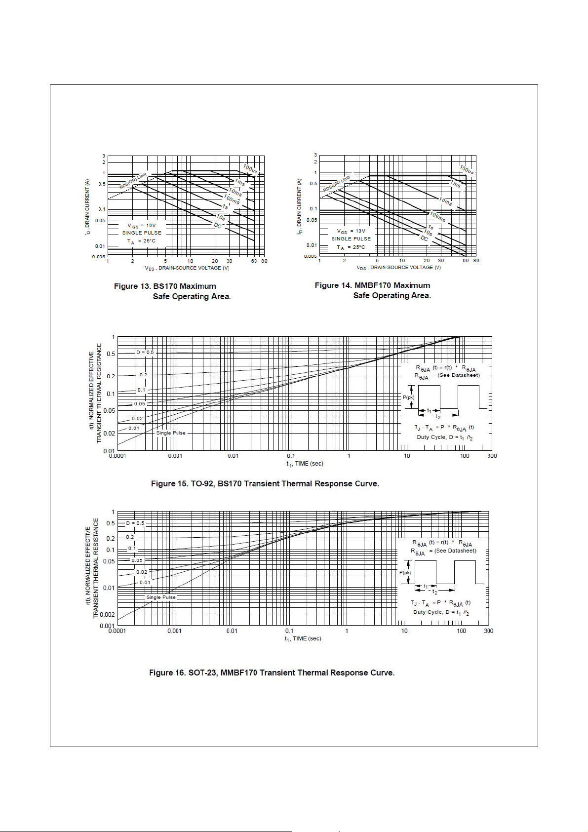
Typical Electrical Characteristics (continued)
BS170 / MMBF170 — N-Channel Enhancement Mode Field Effect Transistor
© 2010 Fairchild Semiconductor Corporation www.fairchildsemi.com
BS170 / MMBF170 Rev. E2 5

BS170 / MMBF170 — N-Channel Enhancement Mode Field Effect Transistor
© 2010 Fairchild Semiconductor Corporation www.fairchildsemi.com
BS170 / MMBF170 Rev. E2 6

BS170 / MMBF170 — N-Channel Enhancement Mode Field Effect Transistor
© 2010 Fairchild Semiconductor Corporation www.fairchildsemi.com
BS170 / MMBF170 Rev. E2 7

BS170 / MMBF170 — N-Channel Enhancement Mode Field Effect Transistor
© 2010 Fairchild Semiconductor Corporation www.fairchildsemi.com
BS170 / MMBF170 Rev. E2 8

BS170 / MMBF170 — N-Channel Enhancement Mode Field Effect Transistor
© 2010 Fairchild Semiconductor Corporation www.fairchildsemi.com
BS170 / MMBF170 Rev. E2 9

Mechanical Dimensions ( TO-92 )
BS170 / MMBF170 — N-Channel Enhancement Mode Field Effect Transistor
TO-92
Dimensions in Millimeters
© 2010 Fairchild Semiconductor Corporation www.fairchildsemi.com
BS170 / MMBF170 Rev. E2 10

SOT-23 Std Tape and Reel Data
SOT23-3L Packaging
Configuration: F igure 1.0
BS170 / MMBF170 — N-Channel Enhancement Mode Field Effect Transistor
Cus tomized Lab el
SOT23-3L Packaging Information
Packaging Option
Packaging type
Qty per Reel/Tube/Bag 3,000 10,000
Reel Size
Box Dimension (mm) 193x 183x 80 355x 333x4 0
Max qty per Box 15, 000 30,000
Weight per unit (gm ) 0.0082 0.0082
Weight per Reel (kg) 0. 1175 0. 4006
Note/Comments
S tandard
(no flow code)
TN R
7" Di a
D87Z
TN R
13"
Antis tatic Cover Tape
F63TNR Lab el
Packaging Description:
S OT23- 3L parts ar e shipped i n tape. The carrier t ape is
made from a dis s ipative ( carbon filled) polyc arbonate
res in. T he cove r tape i s a m ultilayer film (H eat Ac tivated
Adhes ive in nat ure) pr imarily c omposed of pol yester film,
adhes ive l ayer, s ealan t, and anti- static s prayed ag ent.
Thes e re eled parts in s tandard option ar e shipped with
3,000 units per 7" or 177mm diamete r reel. The r eels ar e
dark blue in color and is made o f polystyrene p las tic (antistatic coated) . O ther option come s in 10, 000 units per 13"
or 330c m diameter reel. T his and s ome other options ar e
desc ribed in the P a cka ging Information table.
Thes e f ull reels are i ndividually labeled and placed inside
a s tandard imme diate box made o f r ecyclable corrugated
brown paper w ith a F airc hild l ogo printing. O ne box
contains five r eels maximum. And these immediate boxes
are placed ins ide a labe led s hipping box w hich comes in
E mbosse d
Carri er Tape
different s izes depending on the number of pa rts s hipped.
3P 3P 3P 3P
SOT23-3L Unit Orientation
B arcode L a bel
B arcode
355m m x 333m m x 40m m
Lab el
Intermedi ate c ontainer f or 13" re el option
B arcode L a bel s ample
LO T: CB VK 741B 019
FS I D: MMS Z5221B
D/C1: D9842AB QT Y1: SPEC REV:
D/C2: Q TY 2: CP N:
FA IRCHI LD S E MIC ONDUCT OR C O RP O RA TIO N (F63 TNR)
QT Y: 3000
SPEC :
B arcode
Lab el
193m m x 183m m x 80m m
P izza B ox for S tandard O ption
SOT23-3L Tape Leader and Trailer
Configuration: F igure 2.0
C arrier Tape
C over T ape
Tra iler Ta pe
300mm mi nimum or
75 em pty pock ets
©2001 Fairchild Semiconductor Corporation October 2004, Rev. D1
© 2010 Fairchild Semiconductor Corporation www.fairchildsemi.com
BS170 / MMBF170 Rev. E2 11
C omponents
Leade r T ape
500mm mi nimum or
125 empty pockets

SOT-23 Std Tape and Reel Data, continued
SOT23-3L Embossed Carrier Tape
Configuration: Figure 3.0
T
B0
Wc
D0P0 P2
BS170 / MMBF170 — N-Channel Enhancement Mode Field Effect Transistor
D1
E1
W
F
E2
Tc
K0
P1
A0
User Direction of Feed
Dimensions are in millimeter
Pkg type
SOT-23
(8mm)
Notes: A0, B0, and K0 dimensions are determined with respect to the EIA/Jedec RS-481
SOT23-3L Reel Configuration: Figure 4.0
A0 B0 W D0 D1 E1 E2 F P1 P0 K0 T Wc Tc
3.15
2.77
8.0
1.55
1.125
1.75
6.25
+/-0.10
+/-0.10
+/-0.3
+/-0.05
+/-0.125
+/-0.10
rotational and lateral movem ent requirements (see sketches A, B, and C).
B0
20 deg maximum component rotation
Sketch A (Side or Front Sectional View)
Component Rotation
3.50
min
+/-0.05
20 deg maximum
A0
Sketch B (T op View)
Component Rotation
W1 Measured at Hub
4.0
+/-0.1
Typical
component
cavity
center line
Typical
component
center line
Dim A
Max
4.0
+/-0.1
1.30
0.228
+/-0.013
5.2
+/-0.3
0.5mm
maximum
+/-0.10
0.5mm
maximum
Sketch C (Top View)
Component la teral movement
0.06
+/-0.02
Dim A
max
Dim N
See detail AA
7" Diameter Option
B Min
Dim C
13" Diameter Option
See detail AA
W2 max Measured at Hub
W3
Dim D
min
DETAIL AA
Dimensions are in i nches and millimeters
Tape Size
8mm 7" Dia
8mm 13" Dia
Reel
Option
Dim A Dim B Dim C Dim D Dim N Dim W1 Dim W2 Dim W3 (LSL-USL)
7.00
0.059
177.8
13.00
330
1.5
0.059
1.5
512 +0.020/-0.008
13 +0.5/-0.2
512 +0.020/-0.008
13 +0.5/-0.2
0.795
2.165550.331 +0.059/-0.000
20.2
0.795
4.00
20.2
100
8.4 +1.5/0
0.331 +0.059/-0.000
8.4 +1.5/0
0.567
14.4
0.567
14.4
0.311 - 0.429
7.9 - 10. 9
0.311 - 0.429
7.9 - 10. 9
October 2004, Rev. D1
© 2010 Fairchild Semiconductor Corporation www.fairchildsemi.com
BS170 / MMBF170 Rev. E2 12

Mechanical Dimensions ( SOT-23 )
BS170 / MMBF170 — N-Channel Enhancement Mode Field Effect Transistor
SOT-23
Dimensions in Millimeters
© 2010 Fairchild Semiconductor Corporation www.fairchildsemi.com
BS170 / MMBF170 Rev. E2 13

TRADEMARKS
®
®
®
The following includes registered and unregistered trademarks and service marks, owned by Fairchild Semiconductor and/or its global subsidiaries, and is not
intended to be an exhaustive list of all such trademarks.
AccuPower¥
Auto-SPM¥
Build it Now¥
CorePLUS¥
CorePOWER¥
CROSSVOLT¥
CTL¥
Current Transfer Logic¥
DEUXPEED
Dual Cool™
EcoSPARK
EfficientMax¥
Fairchild
Fairchild Semiconductor
FACT Quiet Series¥
FACT
FAST
®
®
®
®
®
®
FastvCore¥
FETBench¥
FlashWriter
®
*
FPS¥
F-PFS¥
FRFET
Global Power Resource
SM
Green FPS¥
Green FPS¥ e-Series¥
Gmax¥
GTO¥
IntelliMAX¥
ISOPLANAR¥
MegaBuck¥
MICROCOUPLER¥
MicroFET¥
MicroPak¥
MicroPak2¥
MillerDrive¥
®
MotionMax¥
Motion-SPM¥
OptoHiT™
OPTOLOGIC
OPTOPLANAR
®
®
®
PDP SPM™
Power-SPM¥
PowerTrench
PowerXS™
Programmable Active Droop¥
®
QFET
QS¥
Quiet Series¥
RapidConfigure¥
¥
Saving our world, 1mW/W/kW at a time™
SignalWise¥
SmartMax¥
SMART START¥
®
SPM
STEALTH¥
SuperFET¥
SuperSOT¥-3
SuperSOT¥-6
SuperSOT¥-8
SupreMOS¥
SyncFET¥
Sync-Lock™
®
*
The Power Franchise
TinyBoost¥
TinyBuck¥
TinyCalc¥
®
TinyLogic
TINYOPTO¥
TinyPower¥
TinyPWM¥
TinyWire¥
TriFault Detect¥
TRUECURRENT¥*
PSerDes¥
®
UHC
Ultra FRFET¥
UniFET¥
VCX¥
VisualMax¥
XS™
* Trademarks of System General Corporation, used under license by Fairchild Semiconductor.
DISCLAIMER
FAIRCHILD SEMI CONDUCTOR RESERVES THE RIGHT TO M AKE CHANGES WITHOUT FURTHER NOTICE TO ANY PRODUCTS HEREIN TO I MPROVE
RELIABILITY, FUNCTION, OR DESI GN. FAI RCHILD DOES NO T ASSUME ANY LI ABILI TY ARISI NG OUT OF THE APPLI CATION OR USE O F ANY PRODUCT OR
CIRCUIT DESCRIBED HEREIN; NEI THER DOES IT CONVEY ANY LICENSE UNDER I TS PATENT RIGHTS, NOR THE RIGHTS OF OTHERS. THESE
SPECIFICATIONS DO NOT EX PAND THE TERMS OF F AIRCHIL D’S WORLDWIDE TERMS AND CONDITIONS, SPECIFI CALLY THE WARRANTY THEREIN,
WHICH COVERS THESE PRODUCTS.
LIFE SUPPORT POLICY
FAIRCHILD’S PRODUCTS ARE NOT AUTHORIZED FOR USE AS CRI TICAL COM PONENTS IN LI FE SUPPORT DEVI CES OR SYSTEM S WITHOUT THE
EXPRESS WRITTEN APPROVAL OF FAIRCHILD SEM I CONDUCTOR CORPORATI ON.
As used herein:
1. Life support devices or systems are devices or systems which, (a) are
intended for surgical implant into the body or (b) support or sustain life,
and (c) whose failure to perform when properly used in accordance
with instructions for use provided in the labeling, can be reasonably
expected to result in a significant injury of the user.
2. A critical component in any component of a life support, device, or
system whose failure to perform can be reasonably expected to
cause the failure of the life support device or system, or to affect its
safety or effectiveness.
ANTI-COUNTERFEITING POLICY
Fairchild Semiconductor Corporation's Anti-Counterfeiting Policy. Fairchild's Anti-Counterfeiting Policy is also stated on our external website, www.fairchildsemi.com,
under Sales Support.
Counterfeiting of semiconductor parts is a growing problem in the industry. All manufacturers of semiconductor products are experiencing counterfeiting of their parts.
Customers who inadvertently purchase counterfeit parts experience many problems such as loss of brand reputation, substandard performance, failed applications,
and increased cost of production and manufacturing delays. Fairchild is taking strong measures to protect ourselves and our customers from the proliferation of
counterfeit parts. Fairchild strongly encourages customers to purchase Fairchild parts either directly from Fairchild or from Authorized Fairchild Distributors who are
listed by country on our web page cited above. Products customers buy either from Fairchild directly or from Authorized Fairchild Distributors are genuine parts, have
full traceability, meet Fairchild's quality standards for handling and storage and provide access to Fairchild's full range of up-to-date technical and product information.
Fairchild and our Authorized Distributors will stand behind all warranties and will appropriately address any w arranty issues that may arise. F airchild will n ot provide
any warranty coverage or other assistance for parts bought from Unauthorized Sources. Fairchild is committed to combat this global problem and encourage our
customers to do their part in stopping this practice by buying direct or from authorized distributors.
PRODUCT STATUS DEFINITIONS
Definition of Terms
Datasheet Identification Product Status Definition
Advance Information Formative / In Design
Preliminary First Production
No Identification Needed Full Production
Obsolete Not In Production
Datasheet contains the design specifications for product development. Specifications may change in
any manner without notice.
Datasheet contains preliminary data; supplementary data will be published at a later date. Fairchild
Semiconductor reserves the right to make changes at any time without notice to improve design.
Datasheet contains final specifications. Fairchild Semiconductor reserves the right to make changes
at any time without notice to improve the design.
Datasheet contains specifications on a product that is discontinued by Fairchild Semiconductor.
The datasheet is for reference information only.
Rev. I47
© Fairchild Semiconductor Corporation www.fairchildsemi.com

 Loading...