

Page 1

MITSUMI
1432
8567
VSOP-8A
Sense Current Amplifier MM1380
Sense Current Amplifier
Monolithic IC MM1380
Outline
This IC improves on the previous sensor amp MM1089 (Dual). It is a single amp that allows current sensing
regardless of the IC power supply (V
fluctuation rejection ratio have been improved, and gain is switched between 50 and 100 times.
Features
(1) Common mode signal rejection ratio (CMRR1.1kHz) 100dB typ.
(2) Power supply fluctuation rejection ratio (PSRR1.1kHz) 80dB typ.
(3) Operating power supply voltage range +3 ~ +24V
(4) Consumption current 150µA typ.
(5) Voltage gain 50/100 times switching
(6) Input equivalent offset voltage ±0.5mV
(7) Current detection High/Low switching
(8) Single type
CC). Further, the common mode signal rejection ratio and power supply
Package
Package
VSOP-8A
Applications
(1) Notebook PCs
(2) PDA
Pin Assignment
1 ISEL
2 IN
3 IN+
4 GND
5 COM
6 OUT
7 V
8 GSEL
-
CC
Page 2
MITSUMI
Sense Current Amplifier MM1380
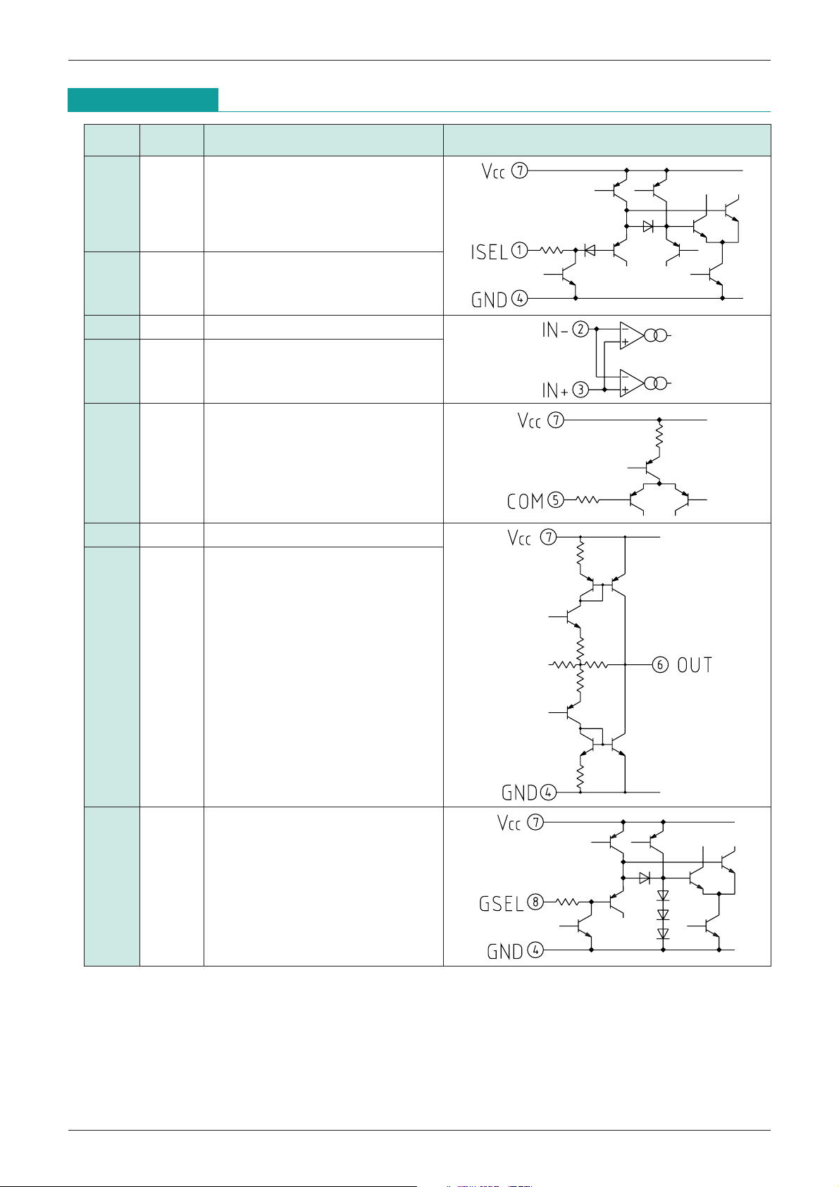
Pin Description
Pin No. Pin name Functions Internal equivalent circuit
1 ISEL Input selection switch terminal
Input common mode voltage range
ISEL="H" : from 1.8V to 24V
ISEL="L" : from
4 GND Ground terminal
2 IN
3 IN+ Non-Inverted input terminal
5 COM Reference voltage input terminal
6 OUT Output terminal
7 VCC Supply voltage terminal
-
Inverted input terminal
-
0.3V to VCC-2.4V
8 GSEL Gain selection switch terminal
Voltage gain
GSEL="H" : Gv=100
GSEL="L" : Gv=50
Page 3

MITSUMI
Block Diagram
Absolute Maximum Ratings
Sense Current Amplifier MM1380
Item Symbol Ratings Units
Storage temperature T
Supply voltage V
CCmax.
Input terminal voltage V
Allowable loss Pd 300 mW
Recommended Operating Conditions
Item Symbol Ratings Units
Operating temperature T
Operating voltage V
STG
Imax.
OPR
CC +3~+24 V
-
40~+125 °C
-
0.3~+25 V
-
0.3~+25 V
-
20~+85 °C
Page 4
MITSUMI
Sense Current Amplifier MM1380
Electrical Characteristics
Item Signal Measurement conditions Min. Typ. Max. Unit
Supply voltage range V
Supply current I
Voltage gain 1 ( 100) G
Voltage gain 2 ( 50) GV2 Vgsel=0V 48.5 50 51.5
Input offset voltage 1 (High side)
Input offset voltage 2 (Low side)
Temperature coefficient of Voff 1
Temperature coefficient of Voff 2
I
nput common mode
voltage range 1 (High side)
Input common mode
voltage range 2 (Low side)
Input differential voltage Vidf
Input bias current 1 (High side)
Input bias current 2 (Low side)
(Except where otherwise indicated, Ta=25°C, VCC=5V, Vicm=15V, Vcom=25V, Visel=5V, Vgsel=5V, R
CC Vcom=VCC/2 3 24 V
CC VIN=0V, RL : OPEN 150 200 µA
V1 Vgsel=5V 97 100 103
L
=10kΩ)
mV/mV
mV/mV
VOFF1VIN=0V, Visel=5V
VOFF2VIN=0V, Visel=0V
VOFF1 Visel=5V
VOFF2 Visel=0V
-
0.5 0.5 mV
-
0.5 0.5 mV
-
44
-
66
µV/°C
µV/°C
Vicm1 Visel=5V 1.8 24 V
Vicm2 Visel=0V
-
0.3
-
200 200 mV
VCC-
2.4
V
Ib1 Visel=5V, VIN=0V 0.8 1.2 1.6 µA
Ib2 Visel=0V, VIN=0V
-
0.8-1.2-1.6 µA
Input impedance Zi 100 kΩ
COM terminal voltage range Vcom R
L : OPEN 1.2
VCC-
1.2
ISEL terminal current Iisel Visel=5V 1.0 µA
ISEL terminal
Visel1 1.7 24 V
voltage range 1 (High side)
ISEL terminal
Visel2 0 0.5 V
voltage range 2 (Low side)
GSEL terminal sink current Igsel Vgsel=5V 1.0 µA
GSEL terminal
Vgsel1 1.7 24 V
voltage range 1 ( 100)
GSEL terminal
Vgsel2 0 0.5 V
voltage range 2 ( 50)
Output voltage range V
Output source current Isrc V
Output sink current Isnk V
Cut off frequency 1 (GV1=100)
Cut off frequency 2 (G
V2=50) FC2 Vgsel=0V, VOUT=
OUT RL : OPEN 0.3
OUT=VCC
-
0.3V 0.5 1.0 mA
OUT=0.3V
-
0.5-1.0 mA
VCC-
0.3
FC1 Vgsel=5V, VOUT=-3dB 100 kHz
-
3dB 140 kHz
Supply voltage
PSRR1 f=1kHz, Visel=5V 70 80 dB
rejection ratio 1 (High side)
V
V
Supply voltage
rejection ratio 2 (Low side)
Common mode
rejection ratio 1 (High side)
Common mode
rejection ratio 2 (Low side)
PSRR2 f=1kHz, Visel=0V 70 80 dB
CMRR1 f=1kHz, Visel=5V 70 80 dB
CMRR2 f=1kHz, Visel=0V 70 80 dB
Page 5
MITSUMI
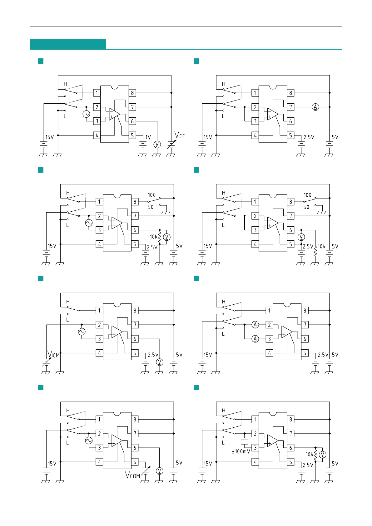
Measuring Circuit
Supply voltage range Supply current
Voltage gain Offset voltage
Sense Current Amplifier MM1380
Input common mode voltage range Input bias current
COM terminal voltage range Output voltage range
Page 6
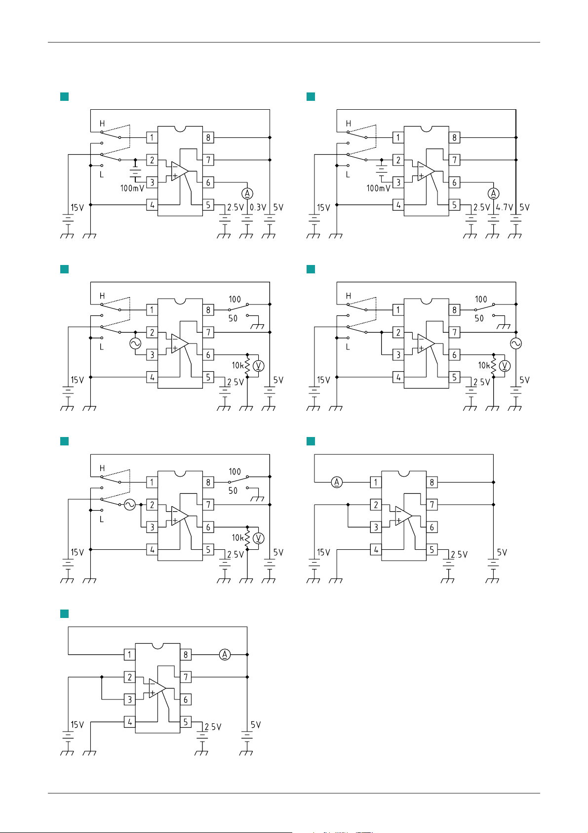
MITSUMI
Sense Current Amplifier MM1380
Output source current Output sink current
Cut off frequency Supply voltage rejection ratio
Common mode rejection ratio ISEL terminal sink current
GSEL terminal sink current
Page 7
MITSUMI
0.0 0.5 1.0 1.5 2.0 2.5
0.0
0.2
0.4
0.6
0.8
1.0
Vcom (V)
V
OUT (min.)
-
Vcom
VOUT (min.) (V)
R1=OPEN
R1=20k
R1=10k
R1=5.1k
-
0.25-0.20-0.15-0.10-0.05 0.00 0.05 0.10 0.15 0.20 0.25
0. E+00
1. E
-
06
2. E
-
06
3. E
-
06
4. E
-
06
5. E
-
06
6. E
-
06
7. E
-
06
VINDiff (V)
IINBais (A)
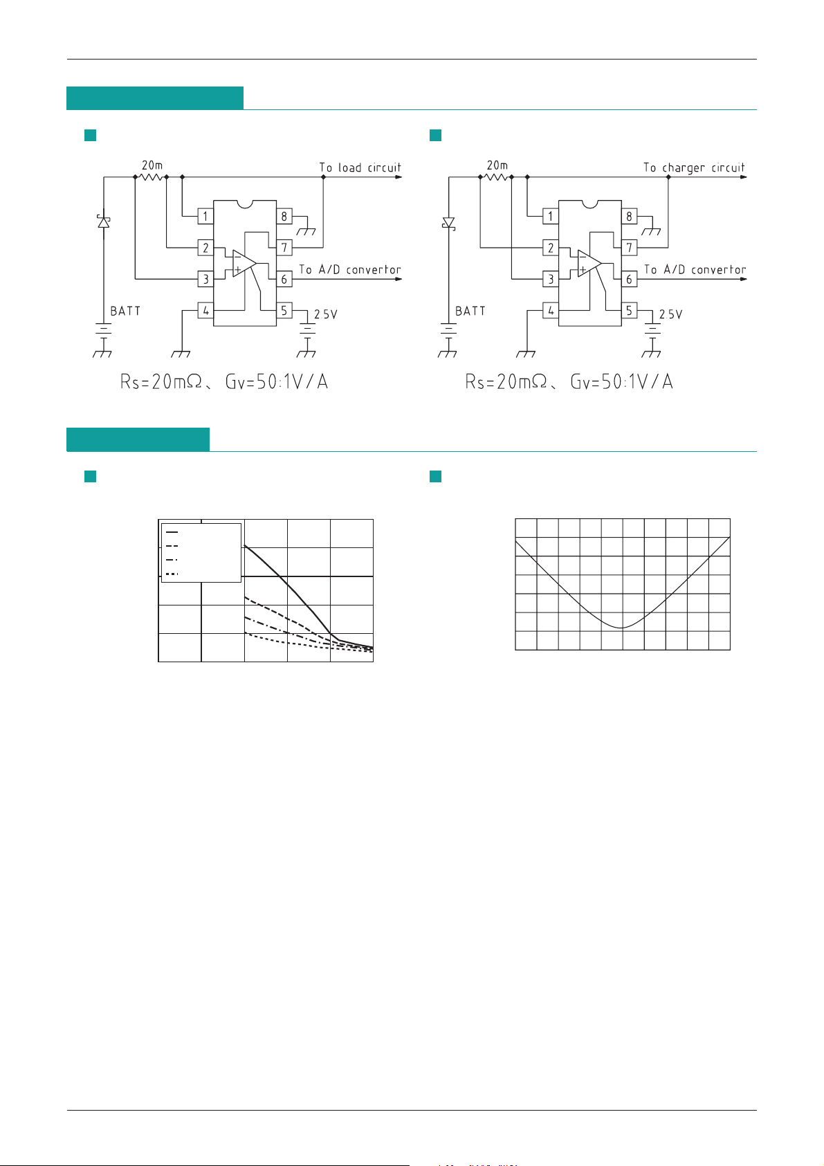
Sense Current Amplifier MM1380
Application Circuit
Battery current sensing circuit Charger current sensing circuit
Characteristics
Minimum output voltage-COM terminal voltage
Input bias current-differential input voltage
 Loading...