

MITSUMI
6-Input 1-Output Video Switch MM1140
6-Input 1-Output Video Switch
Monolithic IC MM1140
Outline
This is a 6-input, 1-output high performance video switch for TV/BS signal switching. It is ideal for use when
multiple input circuits are needed on 1 chip.
Features
1. Built-in mute function (mute pin : input possible)
2. Crosstalk
-
70dB (at 4.43MHz)
3. Power supply voltage 5~13V
4. Frequency response 10MHz
Package
SOP-14B (MM1140XF)
Applications
1. TV
2. VCR
3. Other video equipment
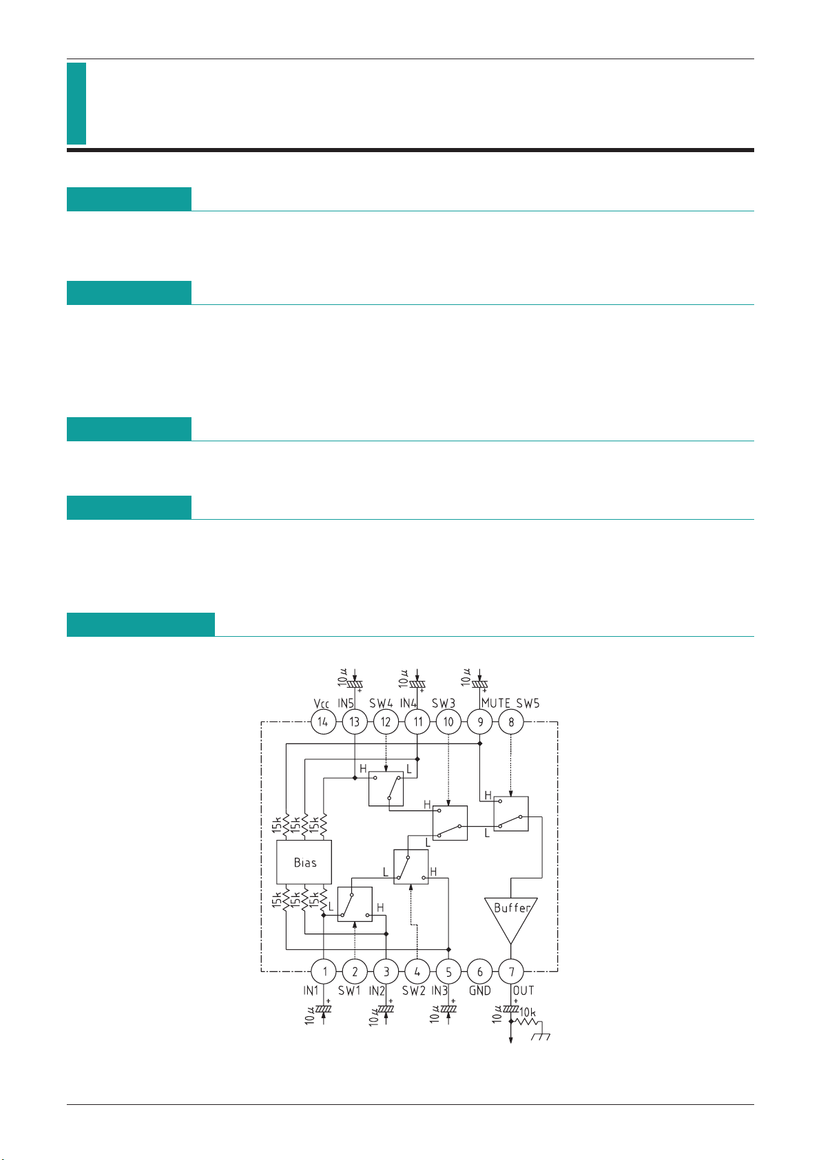
Block Diagram
MITSUMI
6-Input 1-Output Video Switch MM1140
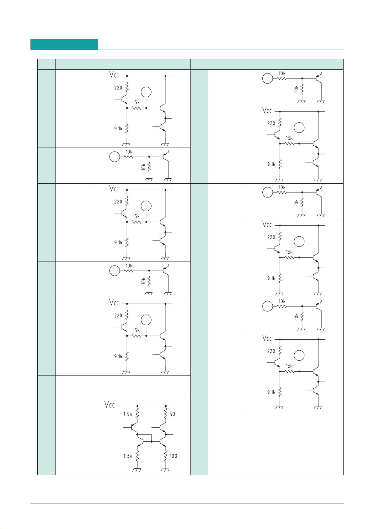
Pin Description
Pin no.
Pin name
Internal equivalent circuit diagram
Pin no.
Pin name
Internal equivalent circuit diagram
1 IN1
2 SW1
3 IN2
4 SW2
5 IN3
6 GND
7 OUT
8 SW5
9 MUTE
10 SW3
11 IN4
12 SW4
13 IN5
14 VCC

MITSUMI
6-Input 1-Output Video Switch MM1140
Absolute Maximum Ratings
(Ta=25°C)
Item Symbol Ratings Units
Storage temperature T
STG
-
40~+125 °C
Operating temperature T
OPR
-
20~+75 °C
Power supply voltage V
CC 15 V
Allowable loss Pd 350 mW
Electrical Characteristics
(Except where noted otherwise, Ta=25°C, VCC=5.0V)
Item Symbol Measurement conditions Min. Typ. Max. Units
Operating power supply voltage range V
CC 4.75 5.0 13.0 V
Consumption current Id Refer to Measuring Circuit 9.0 13.0 mA
Voltage gain G
V Refer to Measuring Circuit
-
0.5 0 +0.5 dB
Frequency characteristic F
C Refer to Measuring Circuit
-
10+1dB
Differential gain DG Refer to Measuring Circuit 0 ±3 %
Differential phase DP Refer to Measuring Circuit 0 ±3 deg
Crosstalk C
T Refer to Measuring Circuit
-
70-60 dB
Total harmonic distortion THD Refer to Measuring Circuit 0.01 0.3 %
Output offset voltage Voff Refer to Measuring Circuit ±30 mV
Switch input voltage
H V
IH Refer to Measuring Circuit 2.1 V
L V
IL Refer to Measuring Circuit 0.7 V
Input impedance Ri 15 kΩ
Output impedance Ro 25 Ω

MITSUMI
6-Input 1-Output Video Switch MM1140
Measuring Procedures
(Except where noted otherwise, VCC=5.0V, VC1=VCC, VC2=0V)
Item
Symbol
Switch
Measuring Procedure
state
Consumption current Id 1
Voltage gain G
V 2
Frequency
F
C 2
characteristic
Differential gain DG 2
Differential phase DP 2
Total harmonic
THD 2
distortion
Output offset voltage Voff 3
Crosstalk C
T 9
H V
IH1
Switch 1
4
input voltage
L V
IL1
H V
IH2
Switch 2
5
input voltage
L V
IL2
H V
IH3
Switch 3
6
input voltage
L V
IL3
H V
IH4
Switch 4
7
input voltage
L V
IL4
H V
IH5
Switch 5
8
input voltage
L V
IL5
Connect a DC ammeter to the V
CC pin and measure. VCC is 5V and
the ammeter is shorted for use in subsequent measurements.
Input a 2.0V
P-P, 100kHz sine wave to SG, and obtain GV from the
following formula given TP12 voltage as V1 and TP14 voltage as V2.
G
V=20LOG (V2/V1) dB
For the above G
V measurement, given TP14 voltage for 10MHz as
V3, F
C is obtained from the following formula.
F
C=20LOG (V3/V2) dB
Input a 2.0V
P-P
staircase wave to SG, and measure differential gain at TP14.
APL=10~90%
Proceed as for DG, and measure differential phase.
Input a 2.5V
P-P, 1kHz sine wave to SG, connect a distortion meter to
TP14 and measure.
Measure the DC voltage difference of each switch status at TP13.
Assume VC1=2.1V, VC2=0.7V.
Input a 2.0V
P-P
, 4.43MHz sine wave to SG, and given TP12 voltage as V4
and TP14 voltage as V5, C
T
is obtained from the following formula.
CT=20LOG (V5/V4) dB
Impress different optional DC voltages on TP6 and TP7. Gradually
raise from VC3=0V. TP1 voltage when TP7 voltage is output on TP13
is V
IH1. Gradually lower from VC3=VCC. TP1 voltage when TP6
voltage is output on TP13 is V
IL1.
Impress different optional DC voltages on TP6 and TP8. Gradually
raise from VC3=0V. TP2 voltage when TP8 voltage is output on TP13
is V
IH2. Gradually lower from VC3=VCC. TP2 voltage when TP6
voltage is output on TP13 is V
IL2.
Impress different optional DC voltages on TP6 and TP9. Gradually
raise from VC3=0V. TP3 voltage when TP9 voltage is output on TP13
is V
IH3. Gradually lower from VC3=VCC. TP3 voltage when TP6
voltage is output on TP13 is V
IL3.
Impress different optional DC voltages on TP9 and TP10. Gradually
raise from VC3=0V. TP4 voltage when TP10 voltage is output on
TP13 is V
IH4. Gradually lower from VC3=VCC. TP4 voltage when TP9
voltage is output on TP13 is V
IL4.
Impress different optional DC voltages on TP6 and TP11. Gradually
raise from VC3=0V. TP5 voltage when TP11 voltage is output on
TP13 is V
IH5. Gradually lower from VC3=VCC. TP5 voltage when TP6
voltage is output on TP13 is V
IL5.

MITSUMI
6-Input 1-Output Video Switch MM1140
Switch Conditions Table
SW
Conditions
Control switching Input switching
S1 S2 S3 S4 S5 S6 S7 S8 S9 S10 S11
1 00000000000
2 00000100000
10000010000
11000001000
11100000100
11110000010
11111000001
3 Conditions 2 0 0 0 0 0 0
4 20000000000
5 02000000000
6 00200000000
7 00120000000
8 00002000000
9 Combination of all control switching and input switching when no signal is output to TP14.
Control Input-Output Table
SW
OUT
12345
LLL
-
L IN1
HLL
-
L IN2
-
HL
-
L IN3
--
H L L IN4
--
H H L IN5
----
H MUTE

MITSUMI
6-Input 1-Output Video Switch MM1140
Measuring Circuit
 Loading...