

Page 1
MITSUMI
HBS-Compatible Driver and Receiver MM1192
HBS-Compatible Driver and Receiver
Monolithic IC MM1192
Outline
This IC conforms to the HBS (Home Bus) specification (Electronic Industries Association of Japan), and has
functions for the reception and transmission of data. AMI is adopted for the waveforms of signals handled by
the transmission and reception units, designed for connection to twisted-pair lines.
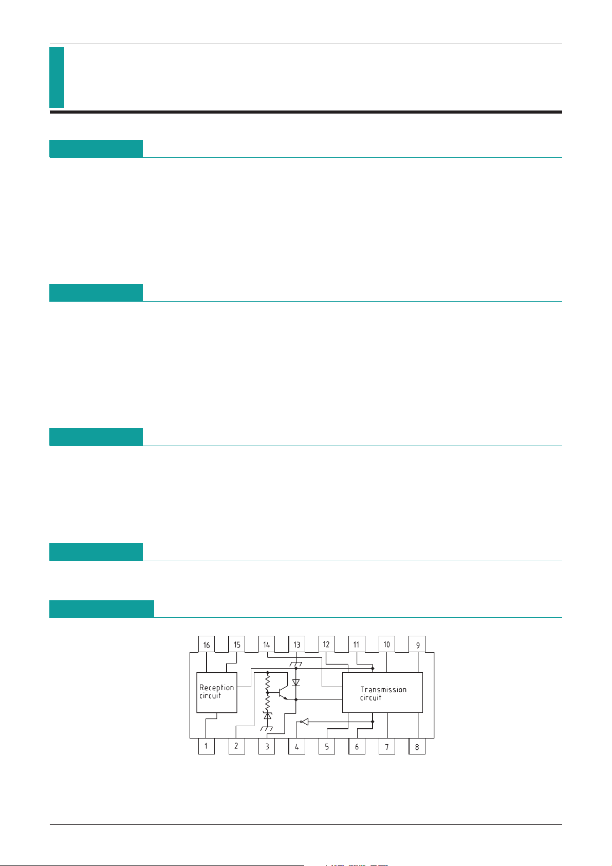
The IC can be driven by a single 5V power supply, and incorporates an output transistor to reduce the
number of external components required.
Telephone equipment, security devices, audio or video equipment, air-conditioning equipment, and a wide
range of other devices can be connected to a bus line to enable mutual communications.
Features
1. Compact design
2. High reliability
3. Replaces pulse transformers
4. Can be driven by a single 5V power supply
5. Low cost
6. Easy circuit design
7. Few external components
Applications
1. Telephony equipment
2. Security equipment
3. Audio and video devices
4. Air-conditioning equipment
5. Wide range of other equipment and devices
Package
DIP-16B (MM1192XD)
Block Diagram
Page 2
MITSUMI
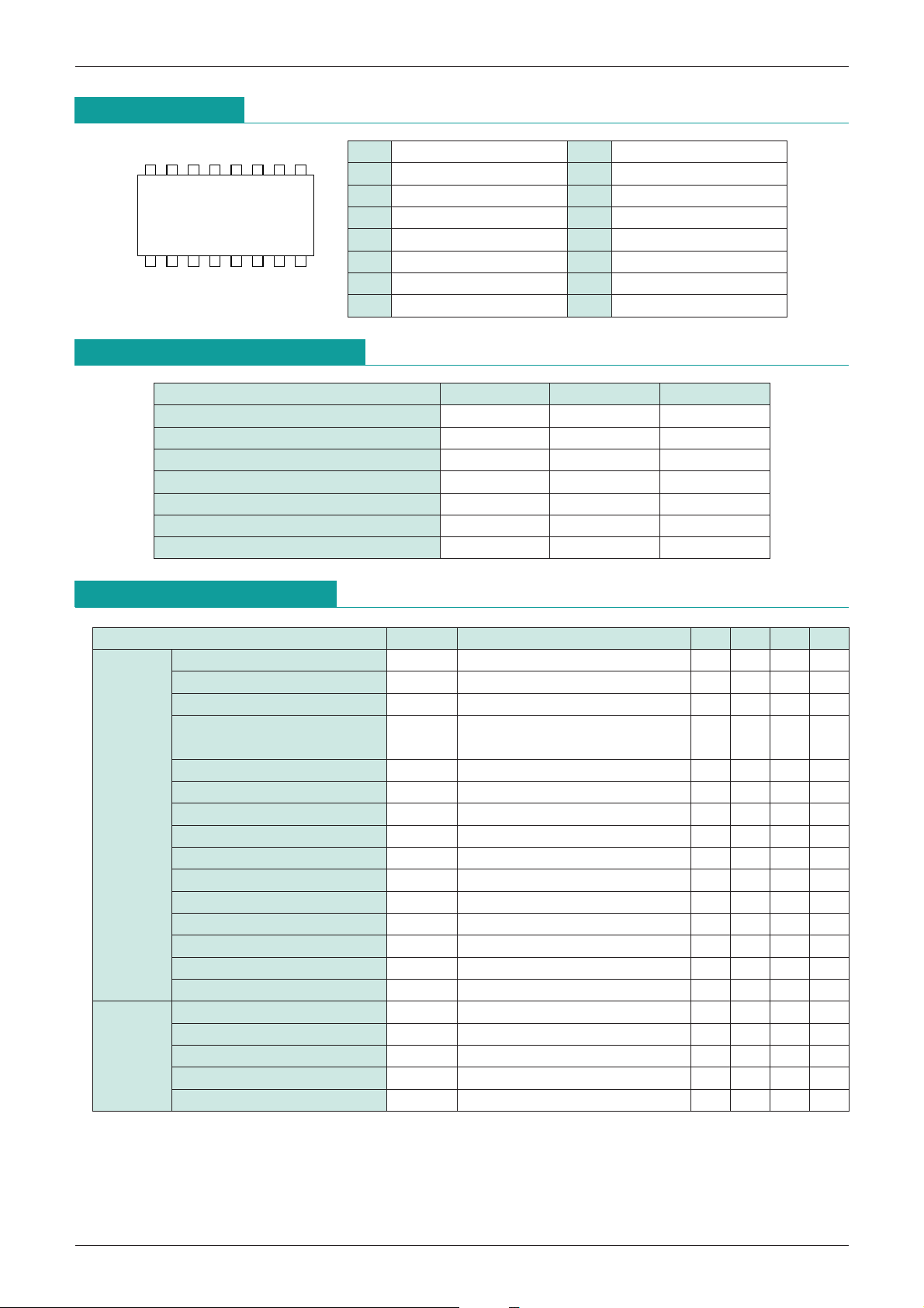
Pin Assignment
16 13 1115 14 12910
13 762458
DIP-16B
HBS-Compatible Driver and Receiver MM1192
1 Reception DATA OUT 9 OUT (A)
2 VIN 10 OUT (B)
3 Boost capacitor pin 11 VCC
4 Boost capacitor pin 12 COLLECTOR (b)
5 RESET 13 GND
6 DATA IN 14 COLLECTOR (a)
7 out (b) 15 IN (2)
8 out (a) 16 IN (1)
Absolute Maximum Ratings
Item Symbol Ratings Units
Storage tempereture T
Operating tempereture T
Power supply voltage V
Operating power supply voltage V
Allowable loss Pd 450 mW
Recommended power supply voltage range
Bias voltage range (V
Electrical Characteristics
Item Symbol Measurement conditions
Power supply current 1 ICCO No signal (5PIN="H") 8 13 mA
Power supply current 2 ICCON
Transmission output voltage V
Transmission waveform
symmetry
Reception sensitivity VRS 0.65 0.75 0.85 VP
Noise resistance VRN
Transmission
Circuits
Input impedance RIN Both pins 15 and 16 25 36 46 kΩ
Transmission delay time 1 T
Transmission delay time 2 T
Transmission delay time 3 T
Transmission delay time 4 T
Reception output H voltage V
Reception output L voltage V
Transmission waveform LOSS 1
Transmission waveform LOSS 2
H level input voltage V
L level input voltage V
H level input current I
L level input current I
Bootstrap output H voltage V
(Except where noted therwise, Ta=25°C, VCC=5V, Ftransmit=10kHz (DUTY=50%) R
(Ta=25°C)
STG
OPR
CC max.
CCOP 4.5~5.5 V
-
40~+125
-
20~+70
-
0.3~+7 V
°
C
°
C
VCCOP2 4.75~5.25 V
IN) VINOP 8.0~40 V
Min. Typ. Max. Units
In transmission FL=10kHz, R
TO Both pins 9 and 10 3.8 4.2 4.6 VP-P
L
=36Ω
75 90 mA
VTR VTO1/VTO2 0.75 1.0 1.25
Level at which no errors are output
d1
d2
d3
d4
ROH 4.5 V
ROL 0.5 V
cf. transmit/receive waveform diagrams
cf. transmit/receive waveform diagrams
cf. transmit/receive waveform diagrams
cf. transmit/receive waveform diagrams
0.55 VP
0.4 µS
0.5 µS
1.0 µS
1.2 µS
VTLS1VT=5V applied, power on 4.5 V
VTLS2VT=5V applied, power off 4.5 V
LIH 2.4 V
LIL 0.6 V
LIH VDATA IN=2.4V 10 µA
LIL VDATA IN=0.4V
BR 7.5 8.0 V
-
300
L
=36Ω)
µA
-
P
-
P
When a negative voltage is applied to pins 7, 8, 9 and 10, there should be no abnormal operation of internal
-
circuits between 0 and 6V. However, if a negative voltage exceeding
6V is applied, thyristor operation may
result, so it is recommended that an external clamping diode be added.
In addition, no measures have been taken for a negative voltage at pins 12 and 14. Hence if a negative
voltage is applied to pins 12 and 14, the internal transistor should not be used.
Page 3
MITSUMI
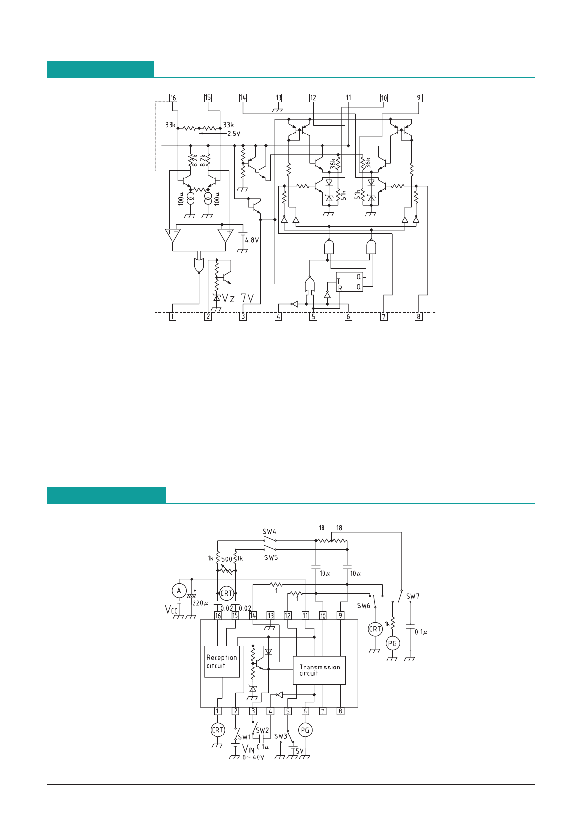
Circuit Diagram
HBS-Compatible Driver and Receiver MM1192
Note 1: The peripheral components in the block diagram are the constants for Ftransmit=10kHz. If the
frequency is low, larger values should be chosen for the coupling capacitors between the receive and
transmit pins and the bus line and for the capacitor connecting pins 3 and 4.
Note 2: A block diagram is shown for an example application in which an external transistor is used; but
depending on system conditions the internal transistor may be used, and no external transistor is
needed. In such cases pins 7 and 8 are left open, a 1Ω resistance is inserted between pins 10 and 12,
and a 1Ω resistance is inserted between pins 9 and 14.
When the load resistance (36Ω) is to be varied during use, these resistances (1Ω) should be changed
according to the load resistance. If these resistances are omitted, oscillation may occur at low volume
levels.
Measuring Circuit
1. No external transistor
Page 4
MITSUMI
RESET
DATA
IN
DATA
OUT
OUT (A)
OUT (B)
Td1
Td3
Td2
Td4
DATA
IN
DATA
OUT
OUT (A)
OUT (B)
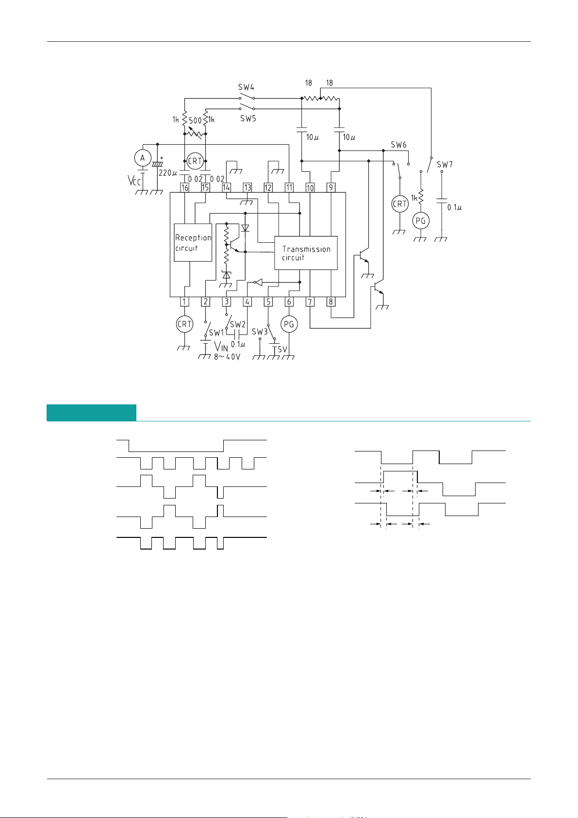
Transmission delay time
2. With external transistor
HBS-Compatible Driver and Receiver MM1192
Timing Chart
 Loading...