

Page 1
MITSUMI
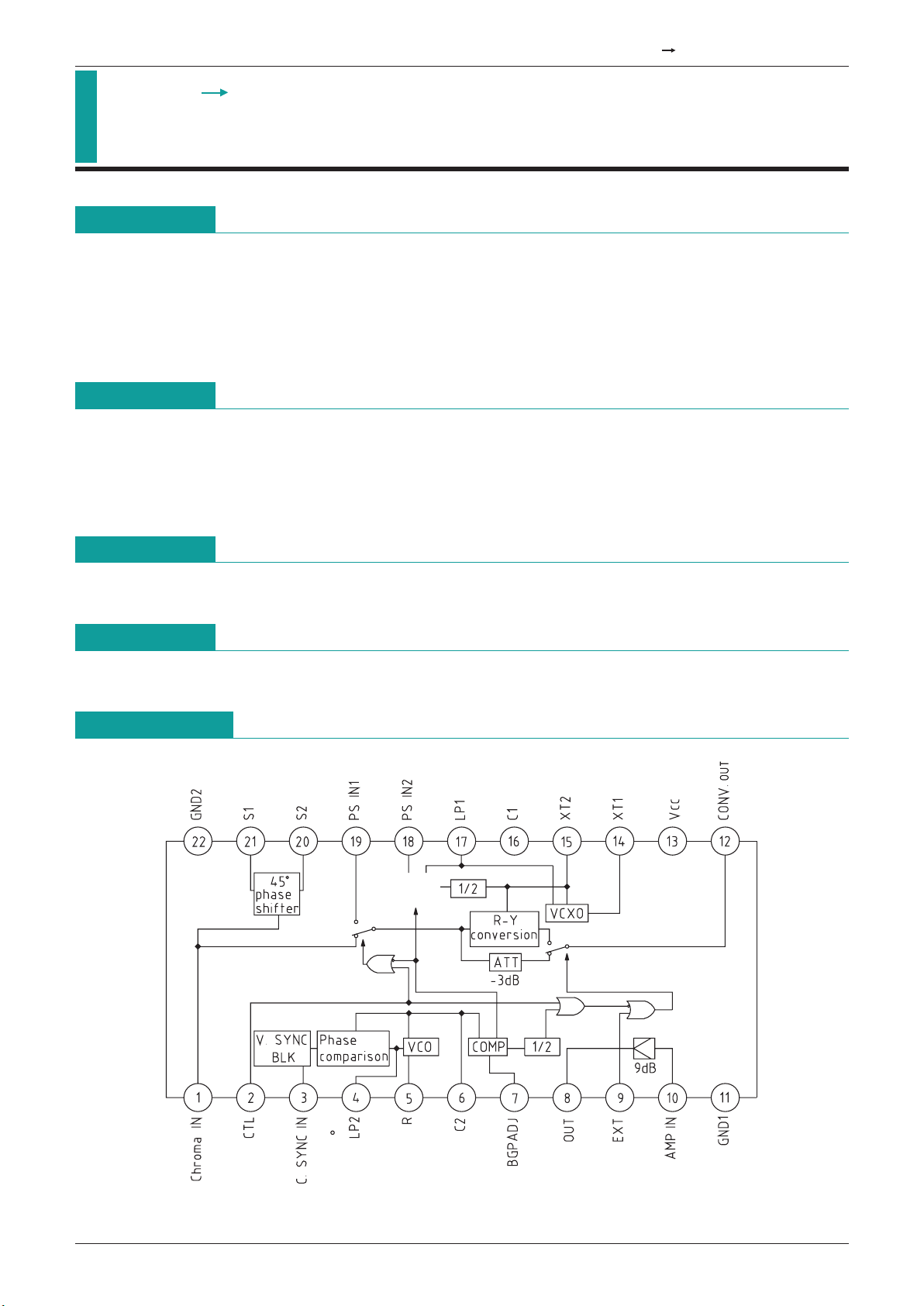
NTSC PAL Converter MM1130
NTSC PAL Converter
Monolithic IC MM1130
Outline
This is an NTSC/PAL signal switching IC.
In PAL conversion mode, a frequency-converted (fc=4.43MHz) NTSC format chroma signal is phase
converted (R-Y axis component is inverted) every 1 hour by shifting burst signal phase by 45°.
Circuit configuration includes VCO (horizontal sync), VCXO (phase conversion carrier), phase conversion
circuit, switches, amps, etc.
Features
1. PAL conversion with phase conversion performed
2. Two possible phase conversion carriers : crystal oscillation and external input
3. No adjustments
4. Four possible mode selections by CTL and EXT pins
Package
SDIP-22A (MM1130XD)
Applications
1. VCR
Block Diagram
Page 2

MITSUMI
NTSC PAL Converter MM1130
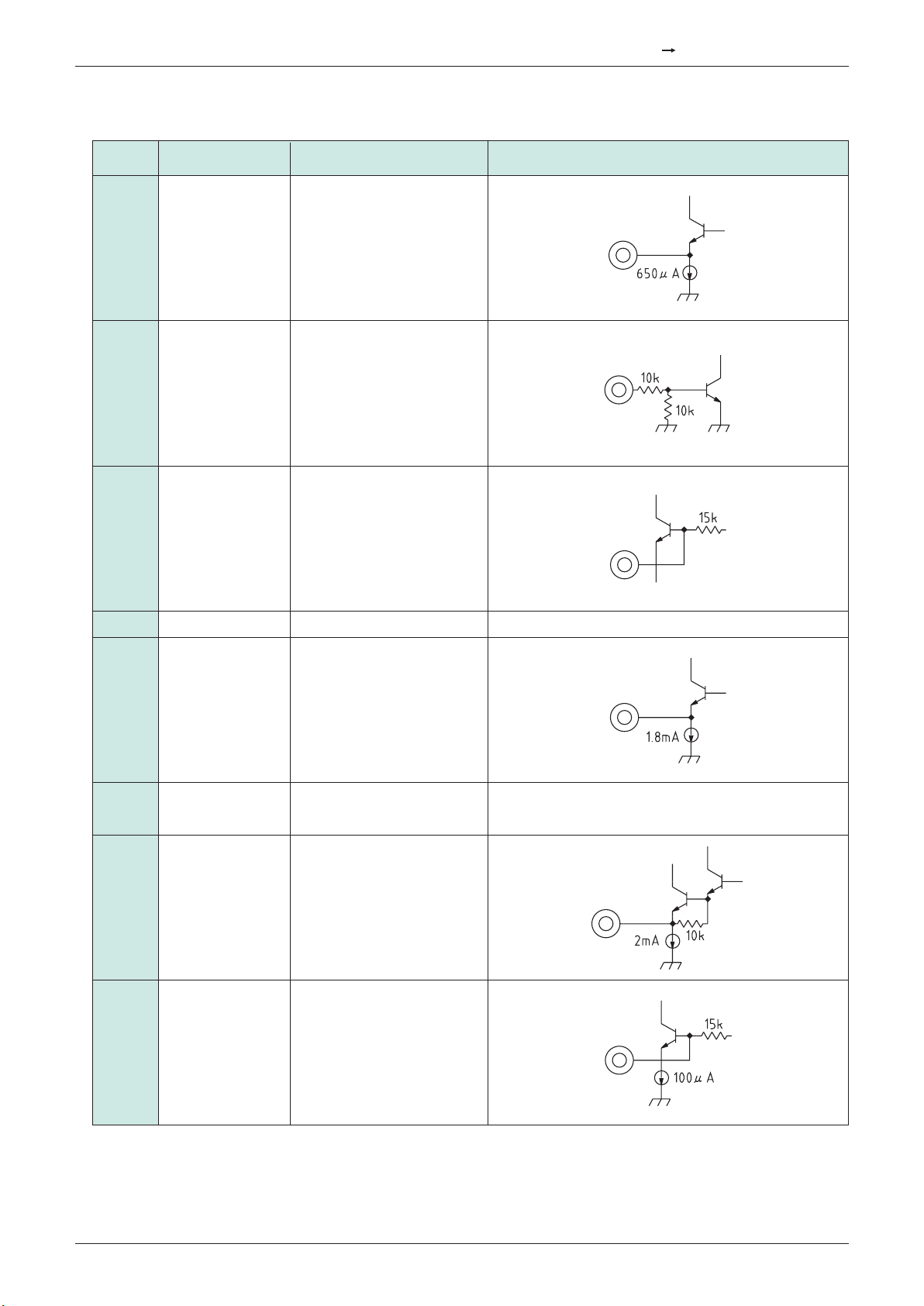
Pin Description
Pin no. Pin name Function Internal equivalent circuit diagram
1 chroma IN Inputs chroma signal
2 CTL Mode setting pin
3 C.SYNC IN Inputs composite sync
signal
4 LP2 Time constant connection
pin for H. SYNC APC loop
LPF
5 R H. SYNC APC feedback pin
6 C2 Pin for connecting H.
SYNC APC free run
frequency setting capacitor
7 BGP ADJ Fine tuning of position for
sampling burst signal. Use
open.
Page 3
MITSUMI
NTSC PAL Converter MM1130
Pin no. Pin name Function Internal equivalent circuit diagram
8 OUT Amp output pin
9 EXT Mode setting pin
10 AMP IN Amp input pin
11 GND1 GND pin
12 CONV.OUT Multiplication circuit output
pin
13 VCC VCC pin.
Inputs 5V.
14 XT1 Carrier (2fsc) oscillation
circuit output pin
15 XT2 Carrier (2fsc) input pin
Page 4

MITSUMI
NTSC PAL Converter MM1130
Pin no. Pin name Function Internal equivalent circuit diagram
16 C1
Carrier APC phase shift pin
17 LP1 Time constant connection
pin for carrier APC loop
LPF
18 PS IN2 Carrier APC input pin. Pin
18 input signal burst signal
and carrier signal are
phase locked.a
19 PS IN1 Burst signal phase input
pin during PAL
conversion.
20 S2 Phase shift circuit output
pin. Signal is Pin 21 output
inverted.
21 S1 Phase shift circuit output
pin. Signal is Pin 20 output
inverted.
22 GND2 GND pin
Page 5

MITSUMI
NTSC PAL Converter MM1130
Absolute Maximum Ratings
(Ta=25°C)
Electrical Characteristics
(Except where noted otherwise, Ta=25°C, VCC=5.0V, SW13 : b)
Item Symbol Ratings Units
Storage temperature T
STG
-
40~+125 °C
Operating temperature T
OPR
-
20~+75 °C
Power supply voltage V
CC max. 7 V
Allowable loss Pd 600 mW
Item
Symbol
Measurement
Measurement conditions Min. Typ. Max.
Units
circuit
Operating power supply voltage
VCC 4.7 5.0 5.3 V
Consumption current I
CC 13 SW2, 9, 13 : a, no input 29.0 40.0 mA
Dynamic range D 0.8 V
P-P
Slew mode (SW2 : b, SW9 : a, VIN1=SG1, VIN3=SG2)
Gain Gt 8
*
1
-
1.0 0 1.0 dB
Phase difference θt8
*
2
-
5 0 5 deg
PAL conversion mode Hn (SW2 : a, SW9 : a, V
IN1=SG1, VIN3=SG2)
*
3
Burst gain G1bt 8
*
1
-
1.0 0 1.0 dB
Red gain G1r 8
*
1
-
1.0 0 1.0 dB
Green gain G1g 8
*
1
-
1.0 0 1.0 dB
Blue gain G1b 8
*
1
-
1.0 0 1.0 dB
Burst phase θ1bt 8 130.0 135.0 140.0 deg
Red phase θ1r 8 98.5 103.5 108.5 deg
Green phase θ1g 8 235.6 240.6 245.6 deg
Blue phase θ1b 8 342.6 347.6 352.6 deg
PAL conversion mode Hn+1 (SW2 : a, SW9 : a, V
IN1=SG1, VIN3=SG2)
*
3
Burst gain G2bt 8
*
1
-
1.0 0 1.0 dB
Red gain G2r 8
*
1
-
1.0 0 1.0 dB
Green gain G2g 8
*
1
-
1.0 0 1.0 dB
Blue gain G2b 8
*
1
-
1.0 0 1.0 dB
Burst phase θ2bt 8
-
145.0-135.0-125.0
deg
Red phase θ2r 8
-
113.5-103.5-93.5
deg
Green phase θ2g 8
-
250.6-240.6-230.6
deg
Blue phase θ2b 8
-
357.6-347.6-337.6
deg
(SW2 : a, SW9 : a, V
IN1=SG1, VIN3=SG2)
DC step V8
*
440mV
BGP timing t1 8
*
5 3.5 4.3 5.1 µS
BGP width t2 8
*
5 3.7 4.5 5.3 µS
Hn/Hn+1 switching timing t3 8
*
5
-
0.6 0.2 1.0 µS
VCO (SW2 : a, SW9 : a, V
IN1 : N0)
Free-running frequency fo1 6 V
IN3 : GND 14.2 15.7 17.2 kHz
Acquisition range fc1 6 V
IN3 : SG3
*
6 1.5 kHz
VCXO (SW2 : b, SW9 : b)
Free-running frequency fo2 14 V
IN1 : No, VIN3 : 5.0V
8.86 8.86 8.86
6438 7238 8038
MHz
Acquisition range fc2 14 V
IN1 : SG4, VIN3 : SG2
*
7 400 Hz
(SW2 : b, SW9 : b, V
IN1=SG5, VIN3=SG3)
Carrier leak V
C112
*
8
-
20 dB
Control pin input resistance (V
IN1=SG1, VIN3=SG2)
CTL pin switching voltage Vt1 3
Lower pin 3 from 5V.
0.7 1.4 2.1 V
Voltage when pin 8 switches.
EXT pin switching voltage Vt2 9
Lower pin 9 from 5V.
0.7 1.4 2.1 V
Voltage when pin 8 switches.
Page 6

MITSUMI
NTSC PAL Converter MM1130
Input Signals
SG1 Color bar chroma signal f=4.433619MHz V=630mVP
-
P
SG2 C. SYNC signal 0V-5V
SG3 15.74kHz pulse wave f : frequency variation 0V
-
5V
SG4 Color bar chroma signal f : frequency variation V=630mV
P-P
SG5 Continuous sine wave f : 4.433619MHz V=630mVP
-
P
variable
0V
5V
4.7µS
Carrier frequency variable
630mVp-p
SG3 SG4
Notes:
*
1 Gain is calculated by 20log (Pin 8 level/Pin 1 level).
*
2 Phase difference is difference between input and output phases (given B-Y axis as 0°.)
*
3 Hn output is 1 horizontal output after input signal burst is shifted +45°. Hn+1output is 1 horizontal output
after input signal burst is shifted +45°, and that signal is R-Y converted.
*
4 DC step difference is the total of burst sampling step different during PAL conversion and 1H switching
step difference.
*
5 BGP, Hn/Hn + 1 Switching Timing
*
6 This is the smaller of frequency f and horizontal sync signal frequency (fH=15.73khz) difference when the
frequencies are separated sufficiently high and low, then brought closer, and the waveform locks.
*
7 This is the smaller of frequency f and carrier frequency (fC=4.433619MHz) difference when the frequencies
are separated sufficiently high and low, then brought closer, and the waveform locks.
*
8 Carrier leak is the 8.86MHz component level at Pin 12.
Vc1=20log (8.86MHz component/4.43MHz component) dB
1H 1H
burst sampling step difference
burst sampling
1H switching step difference
C.SYNC
BGP
Hn/Hn
+1
switching timing
t1
t2
t3
4.7µS
Page 7

MITSUMI
NTSC PAL Converter MM1130
Mode Settings
CTL EXT
L L PAL conversion mode
H L Through mode
H H R-Y conversion mode
L H Hn + 1 (PAL) output mode
Burst
Chroma
R-Y
B-Y
Burst
Chroma
R-Y
B-Y
Burst
Chroma
R-Y
(Hn) (Hn
+1)
B-Y
Burst
Chroma
R-Y
B-Y
Switching every 1H
Burst
Chroma
R-Y
B-Y
PAL conversion mode Through mode
R-Y conversion output mode Hn + 1 (PAL) output mode
Measuring Circuit
Page 8

MITSUMI
NTSC PAL Converter MM1130
Application Circuits
1. For crystal oscillation of 2fsc
2. For external input of 2fsc
2fsc phase
Input burst phase
*
1 Regarding 2fsc input
Input 2fsc with input level of more than
500mV
P-P and phase as shown in the figure
at left.
 Loading...