

Page 1
MITSUMI
1432
8567
SOP-8C/DIP-8B
System Reset (Built-in Watch Dog Timer) MM1099
System Reset (Built-in Watch Dog Timer)
Monolithic IC MM1099
Outline
The function of this IC series MM1099 is to accurately reset systems, a generating reset signal at the time of
instantaneous supply voltage off or lowering in varied CPU and other logic system.
Further, with the watch dog timer built-in it can diagnose the operation of the system, intermittently
generating reset pulses when they operate erroneously to prevent runaway.
Features
1. Built-in watch dog timer
2. Low current consumption 130µA TYP.
3. Low operating threshold voltage V
4. Watch dog stop function (RCT terminal)
5. Long clock monitoring time
T
PR (POWER ON) : TWD (clock monitoring)=1 : 1
6. Fewer outer components
CC=0.8V
Package
DIP-8B (MM1099AD, MM1099BD)
SOP-8C (MM1099AF, MM1099BF)
SIP-8A (MM1099AS, MM1099BS)
Applications
1. Reset circuit for microcomputers, CPU and MPU.
2. Reset circuit for logic circuitry.
3. Monitoring of microcomputer system, etc.
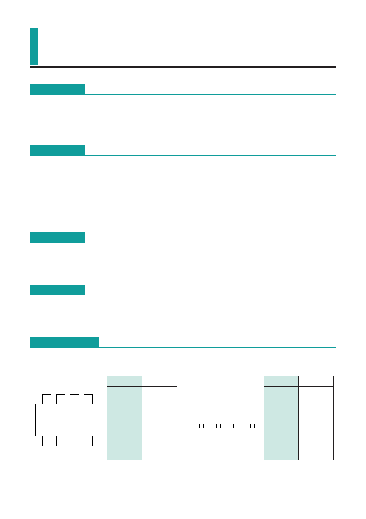
Pin Assignmemt
1 TC
2 N.C
3 CK
4 GND
5 V
CC
13572468
1 TC
2 N.C
3 CK
4 GND
5 V
CC
6 RCT
7 V
8 RESET
S
-----------------------------------------------------------
SIP-8A
6 RCT
7 V
8 RESET
S
-----------------------------------------------------------
Page 2
MITSUMI
Pin Description
System Reset (Built-in Watch Dog Timer) MM1099
Pin No.
Pin name
Variable terminals TWD, TWR and TPR TPR (mS) = 5000 CT (µF)
1 TC
The time for TWD, TWR and TPR to be TWD (mS) = 500 CT (µF)
determined by the external capacitor. T
2 N.C
3 CK
4 GND
5 V
6 RCT
7 V
8 RESET
Clock input terminal Inputs the clock from the logic system.
Ground terminal
CC
Voltage detection MM1099A 3.2V MM1099B 4.2V
Watchdog timer stop pin Operation modes: Operation OPEN, Stop connect to GND
S
Detect voltage variable terminal
Reset output pin (low output)
Absolute Maximum Ratings
Item Symbol Rating Units
Power supply voltage V
CK pin input voltage V
S pin input voltage VVS
V
Voltage applied to RCT pin V
Voltage applied to RESET
Allowable loss Pd 300 mW
Storage temperature T
----------------------------------------------------
CC max.
CK
RCT
pin VOH
STG
Function
WR(mS) = 100 CT (µF)
-
0.3~+10 V
-
0.3~VCC+0.3 (
-
0.3~VCC+0.3 (
-
0.3~VCC+0.3 (
-
0.3~VCC+0.3 (
-
40~+125
<
+10) V
=
<
+10) V
=
<
+10) V
=
<
+10) V
=
°
C
Recommended Operating Conditions
Item Symbol Rating Units
Power supply voltage V
----------------------------------------------------
RESET
sync current IOL 0~1.0 mA
Clock monitoring time setting T
Clock rise and fall times t
TC pin capacitance C
Operating temperature T
CC +2.2~+7.0 V
WD 0.1~1000 mS
FC, tRC <100 µS
T 0.0002~2 µF
OP
-
25~+75
°
C
Page 3
MITSUMI
System Reset (Built-in Watch Dog Timer) MM1099
Electrical Characteristics (DC)
Item Symbol Measurement conditions Min. Typ. Max. Units
Consumption current
Detection voltage
Detection voltage temperature coefficient
Hysteresis voltage
CK input threshold V
CK input current
Output voltage MM1099A
(High) MM1099B 4.0 4.5
Output voltage (Low)
R output sync current I
MM1099A
CC During watchdog timer operation
I
MM1099B 130 195
MM1099A
V
MM1099B 4.05 4.20 4.35
MM1099A
V
MM1099B 4.15 4.30 4.45
VS/ T ±0.01 %/°C
MM1099A
HYS
V
MM1099B 50 100 150
I
I
V
OL1 I =0.5mA, VS=0V 0.2 0.4
V
OL2 I =1.0mA, VS=0V 0.3 0.5
V
OL V =1.0V, VS=0V 1 2 mA
(Except where noted otherwise, MM1099A : V
CC
=3.6V, Ta=25°C, MM1099B : VCC=5.0V)
(100) (150)
µA
SL
SH
VS=OPEN, VCC
VS=OPEN, VCC
3.10 3.20 3.30
3.15 3.25 3.35
25 50 100
VSH-VSL, VCC
TH 0.8 1.2 2 V
IH A : VCK=3.6V, B : VCK=5.0V 0 1
mV
µA
IL VCK=0V
OH
----------------------------------------------------
RESET
I=-1µA, VS=OPEN
----------------------------------------------------
RESET
----------------------------------------------------
RESET
----------------------------------------------------
RESET
-
12-6
3.0 3.4
-
2
V
V
V
T charge current
C
Minimum operating power
supply voltage to ensure RESET
---------------------------------------------------
I
CT1
I
CT2
CCL 0.8 1.0 V
V
VTC=1.0V during watchdog timer operation-0.16-0.24-0.48 µA
VTC=1.0V during power ON reset operation-0.16-0.24-0.48 µA
----------------------------------------------------
RESET
V =0.4V
----------------------------------------------------
RESET
I =0.1mA
Page 4

MITSUMI
System Reset (Built-in Watch Dog Timer) MM1099
Electrical Characteristics (AC)
(Except where noted otherwise, MM1096A : V
CC
=3.6V, Ta=25°C MM1096B : VCC=5.0V)
Item Symbol Measurement conditions Min. Typ. Max. Units
3.6V
2.8V
5.0V
CC input
V
pulse width
MM1099A 8
PI µS
T
MM1099B 8
VCC
VCC
4.0V
CK input pulse width T
CK input cycle T
CKW 3µS
CK 20 µS
CK or
Watchdog timer
T
monitoring time
1
*
WD CT=0.02µF 50 100 150 mS
Reset time for
T
watchdog timer
2
*
WR CT=0.02µF 1 2 3 mS
Reset hold time for
power supply rise *3
Output delay time from V
Output rise time
Output fall time
CC
*
5 tR RESET
*
5 tF RESET
*
TPR 50 100 150 mS
4
TPD RESET
CT=0.02µF, VCC
----------------------------------------------------------------------
pin, RL=10kΩ, CL=20pF 2 10 µS
----------------------------------------------------------------------
pin, RL=10kΩ, CL=20pF 2.0 4.0 µS
----------------------------------------------------------------------
pin, RL=10kΩ, CL=20pF 0.2 1.0 µS
Notes :
1 The "monitoring time" means the time interval from the last pulse of the clock pulses for timer clear
*
(negative edge) to the output of the reset pulse. If the clock pulse is not input during this time interval, the
reset output will be given.
2 The "reset time" is no other than the reset pulse width, except when resetting the POWER ON.
*
3 The "reset hold time" is the time interval from the time point when VCC exceeds the detect (VSH) at the time
*
of Power On Reset (Power variation reset) to the reset release (RESET
4 The "output delay time" means the time interval from when the supply voltage comes lower than the
*
detect voltage (V
5 The voltage range is 10 to 90% when measuring the output rise and fall times.
*
6 By varying the capacitance of CT, we can vary the watch dog timer monitoring time (TWD), the reset time at
*
the time of the watch dog timer (T
SL) to when comes the reset state (RESET
WR), and the reset hold time at the time of power source rise (TPR). The
-------------------------------------------------
-------------------------------------------------
output "HIGH").
output "Low").
variable time can be expressed by the following formulas:
T
PR (mS)
T
WD (mS)
T
WR (mS)
.
=.5000 CT (µF)
.
=.5000 CT (µF)
.
=.100 CT (µF)
Example : When CT=0.02µF
.
PR
=.100mS
T
.
T
WD
=.100mS
.
T
WR
=.2mS
Page 5

MITSUMI
System Reset (Built-in Watch Dog Timer) MM1099
Measuring Circuits
Measuring Circuit 1 (DC) Measuring Circuit 2 (AC)
Measuring Circuit 1
Item
Consumption current I
Detection voltage
CK input threshold V
CK input current
Symbol
SW & Power Supply Table
-----------------------------------------------
1V
RESET
-
-
-
-
-
-
SW1 SW2 SW3 SW4 SW5 SW6 SW7 VCC VCK VCT I VM, IM Notes
CC OFF OFF OFF ON ON ON A 3.6V 3.6V 0V
SL OFF OFF ON ON ON ON A
V
SH OFF OFF ON ON ON ON A
V
TH OFF OFF OFF ON ON ON A 3.6V
IH OFF OFF OFF ON ON ON A 3.6V 3.6V 0V
I
3.6V 3V
3V 3.6V
0V 2V
0V 2V
0V 3V
IIL OFF OFF OFF ON ON ON A 3.6V 0V 0V
Output voltage (High) VOH ON OFF ON ON ON ON A 3.6V 3.6V 2V-1µA VO1
OL1 ON ON ON ON ON ON A 3.6V 3.6V 2V 0.5mA VO1
Output voltage (Low)
Output sink current I
T charge current 1 ITC1 OFF OFF OFF ON ON OFF A 3.6V
C
CT charge current 2 ITC2 OFF OFF OFF ON ON OFF A 3.6V
Minimum operating power
supply voltage to ensure RESET
Measuring Circuit 2
Item
CC input pulse width TP1C B
V
CK input pulse width T
CK input cycle T
Watchdog timer
monitoring time CRT2
Reset time
for watchdog timer CRT2
Reset hold time for
power supply rise CRT2
Output delay time
CC
from V
Output rise time T
Output fall time T
V
OL2 ON ON ON ON ON ON A 3.6V 3.6V 2V 1.0mA VO1
V
OL1 OFF ON ON ON ON ON B 3.6V 3.6V 2V
VCCL ON OFF ON ON ON ON A
------------------------------------------------------
SW & Power Supply Table
Symbol
SW1 SW2 VCCA VCC VCKA VCK CRT Notes
CKW AB
CK AB
T
WD AA
T
WR AA
PR
B A
T
A
TPD CA
R AA
F AA
3.6V
2.8V
3.6V
0V
T1
-
-
-
-
-
-
-
1.4V
-0V
1.4V
3.6V
0V
1.4V
3.6V
0V
3.6V
3.6V
3.6V
--
3.6V
3.6V
0V 2V
-
-
0V 0V
T2 T3
T2
or
T2 T3
-
-
-
-
-
1V
IV
T2
-
-
-
-
-
-
3.6V
3.6V
3.6V
0V CRT1
3.6V CRT1
3.6V CRT1
ICC
VO1, CRT1
VO1, CRT1
ICK, VCK
ICK
ICK
IO1VO=1V
ITC
ITC
VO1, VCC
CRT1
CRT2
CRT1
CRT2
CRT1
CRT2
CRT1
CRT1
CRT1
T1=8µS
T2=3µS
T3=20µS
Page 6

MITSUMI
1 2
3 455
6
7 8 9 10
11
12
VCC
CK
C
T
RESET
VSL
0.3V
V
SH
TCK
TPR
TWD
TWR
TPR
Block Diagram
System Reset (Built-in Watch Dog Timer) MM1099
Timing Chart
RA RB
MM1099A
MM1099B
~
~
-
305k
350k
Note 1. Cp = approx. 0.1µF
Note 2. C
~
1000pF
-
Note 3. The watchdog timer can be stopped by grounding the RCT pin.
(Function as voltage detection circuit.)
Note 4. T
PR, TWD can be varied by pulling up the RCT pit to VCC using a resisteor.
~
~
-
195k
150k
Page 7

MITSUMI
System Reset (Built-in Watch Dog Timer) MM1099
Description of Operation
1. The RESET
2. Charging starts at the capacitor CT when VCC riset to VSH (MM1099A .=.3.25V, MM1099B .=.4.3V), when the
3. The output reset is released after a given interval T
4. If clock is input into CK terminal while C
5. When the C
6. When the clock ceases and C
7. The reset time at the time of watch dog time T
8. When V
9. C
10.The output reset is released T
11.If power Off occurs, reset is output if V
12.When V
-------------------------------------------------------
Approximately 1µA (Vcc=0.8V) of pull up current is output from RESET
will become "Low" if VCC rises to about 0.8V.
----------------------------------------------------------------
output has been reset.
PR from when the CT Starts charging and to when it
discharges (that is, the time from when C
given value 2 (.=.0.2V). (RESET
(V
CC=0.8V). The reset hold time TPR is expressed by the following formula:
T
PR (ms)
.
=.5000 CT (µF)
After the reset release C
-------------------------------------------------------
T restarts charging and the watch dog timer begins operating.
will become "High"). The RESET will output a pull up current, about 1µA
Note that input of clock while POWER ON RESET time T
T voltage takes a given value 1 (
PR will cause an erroneous operation.
T is charging (negative edge trigger), CT changes from charging
.
=.1.4V) up until decreases to a
over to discharging.
T voltage decreases to a given threshold (
.
=.0.2V), then discharging changes over to charging.
Steps 4 and 5 will be repeated while normal clock is input from the logic system.
reset state (RESET
The C
-------------------------------------------------------
T charging time TWD up until the reset is output (watch dog monitoring time) is expressed by the
becoming "Low").
T voltage reaches the RESET ON threshold (
.
=.1.4V), the output enters into
following formula:
T
WD (ms)
.
=.5000 CT (µF)
WR is the discharging time while the CT voltage lowers down
to the reset off threshold (.=.0.2V). The calculation formula:
T
WR (ms)
After the reset off threshold is reached, the output reset is released and C
.
=.100 CT (µF)
T commences to charge. If
thenceforth the clock is input normally, steps 4 and 5 will be repeated, and setps 6 and 7 repeated if the
clock ceases.
CC lowers down to VSL (MM1099A
C
T charged.
T discharging starts when VCC rises up to VSH.
If V
CC lower instantaneously, charging starts after load discharging of CT if the time interval from when VCC
.
=.3.2V, MM1099B .=.4.2V), the reset is output. At the same time
comes lower than VSL up until when it rises to VSH or higher is equal or superior to the reference value of
V
CC input pulse width TPI.
PR after VCC becomes VSH or higher, and the watch dog time will start. Then if
V
CC becomes VSL or lower, steps 8 to 10 will be repeated.
CC becomes VSL or lower.
CC comes down to 0V, the reset output will hold up until VCC becomes 0.8V.
 Loading...