

Page 1
MITSUMI
No-adjustment Sync Separator + Sync Detector MM1067
No-adjustment Sync Separator + Sync Detector
Monolithic IC MM1067
Outline
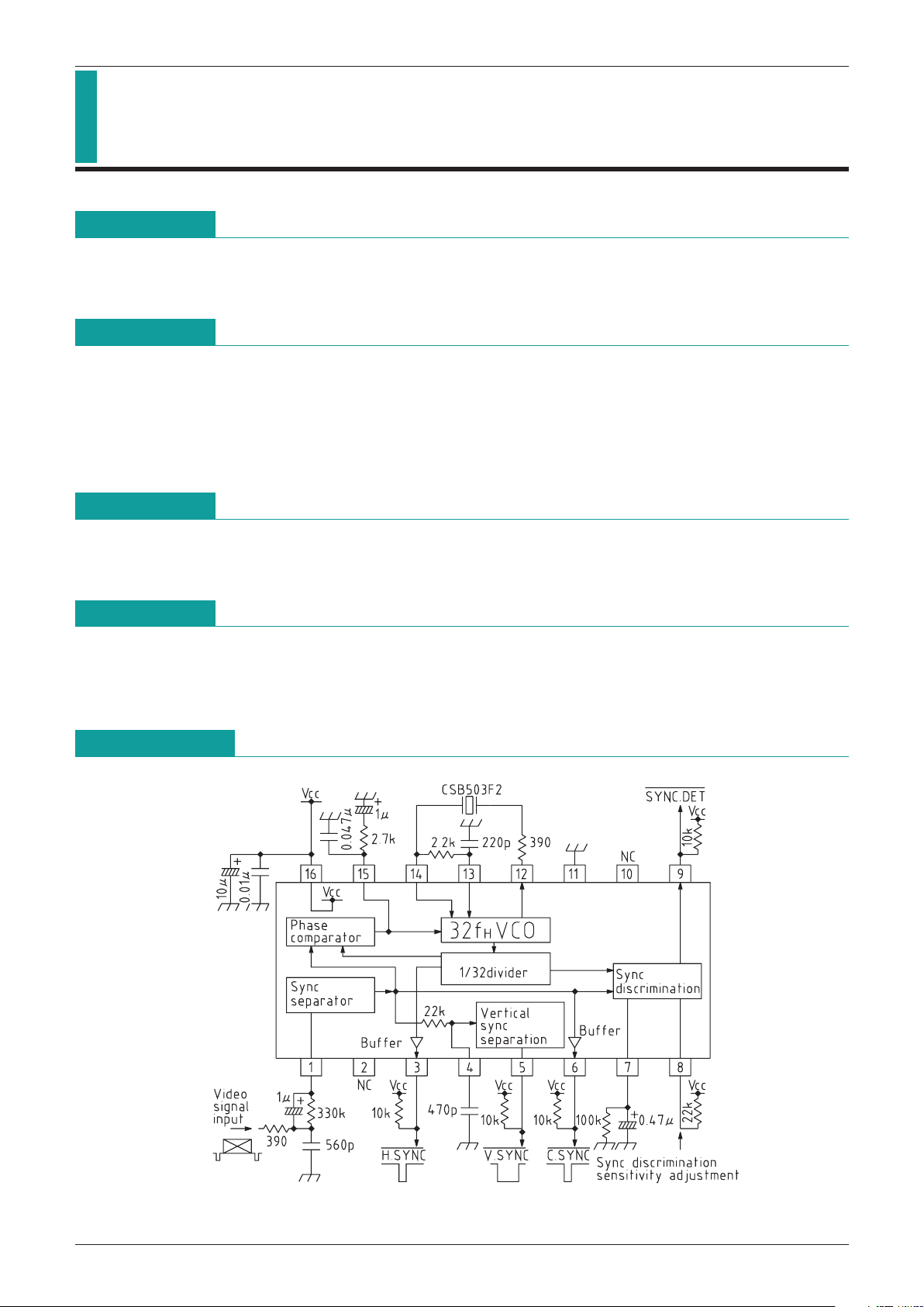
This IC is a no-adjustment sync separator + sync detector designed for use in VCR, TV and other video
equipment.
Features
1. Sync separator with AFC (ceramic resonator means no adjustment required)
2. Composite and sync output pins
3. Sync detection circuit (used for blue-back switching or tuner automatic channel selection, etc.)
4. Power supply voltage V
CC=5V
5. Ceramic resonator can be selected for use in either PAL or NTSC
Package
SOP-16A (MM1067XF)
DIP-16A (MM1067XD)
Applications
1. TV
2. VCR
3. Other video equipment
Block Diagram
Page 2
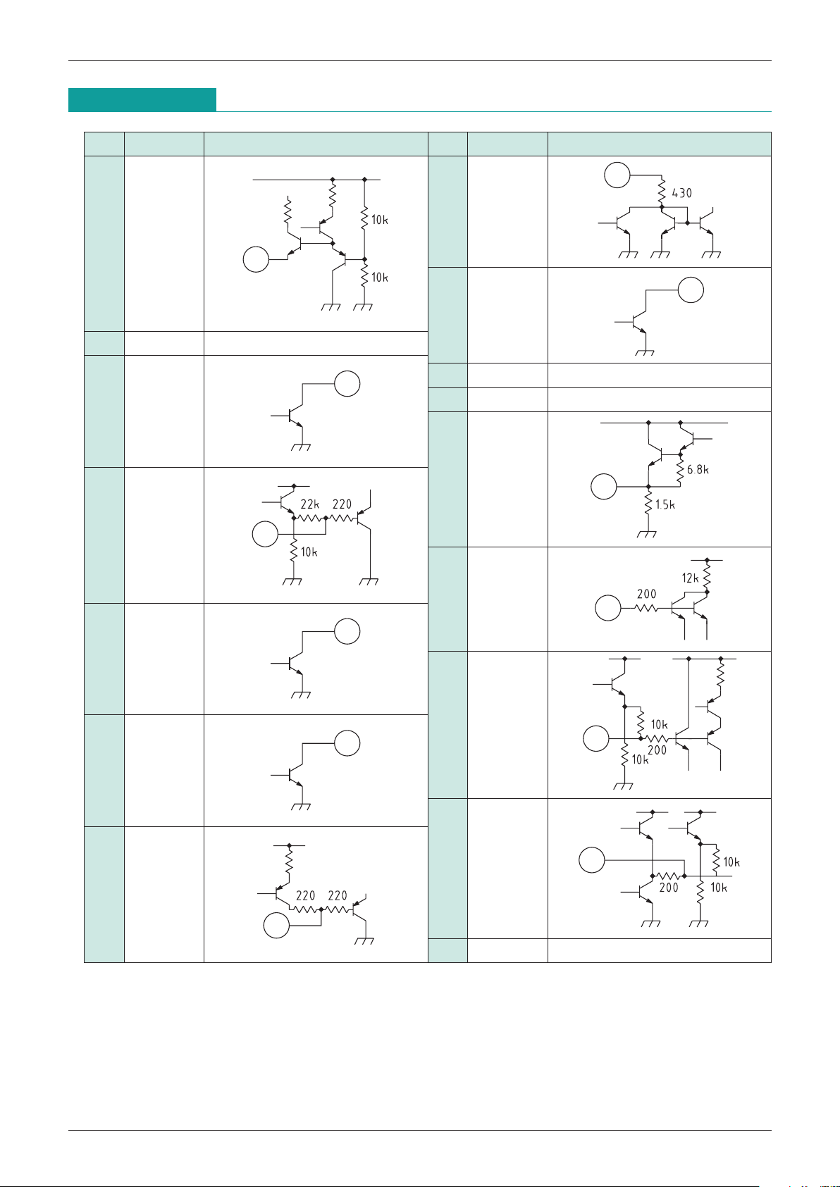
Pin no.
Pin name
Internal equivalent circuit diagram
Pin no.
Pin name
Internal equivalent circuit diagram
MITSUMI
No-adjustment Sync Separator + Sync Detector MM1067
Pin Description
1 Video IN
3 H.SYNC
2 NC
4 V.INT
5 V.SYNC
6 C.SYNC
7 CR
8 GAIN
9 SYNC.DET
12 OSC-OUT
10 NC
11 GND
13 OSC-IN1
14 OSC-IN2
15 LPF
16 VCC
Page 3
MITSUMI
No-adjustment Sync Separator + Sync Detector MM1067
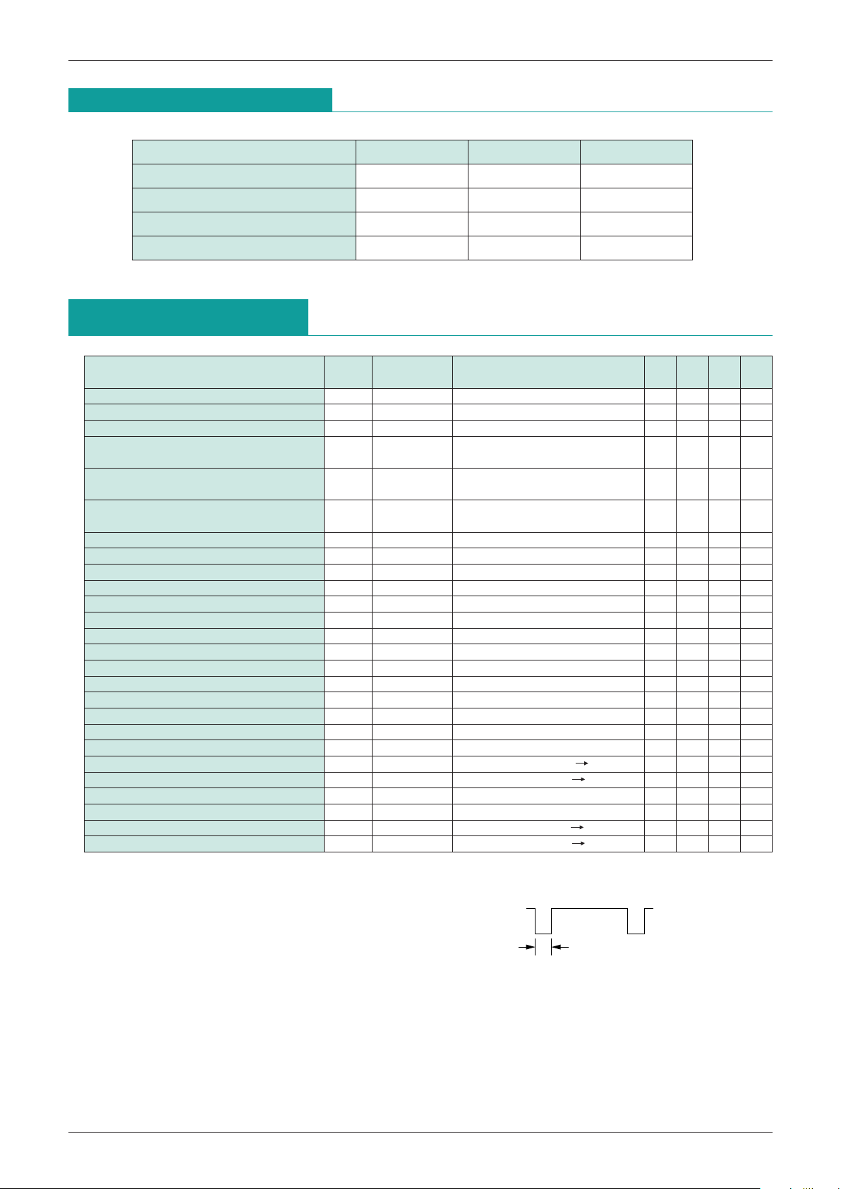
Absolute Maximum Ratings
(Ta=25°C)
Electrical Characteristics
(Except where noted otherwise, Ta=25°C, VCC=5.0V, X=CSB503F2,
R=390 [OHM], C=3300pF, SW1=OFF)
Item Symbol Ratings Units
Storage temperature T
STG
-
40~+125 °C
Operating temperature T
OPR
-
20~+75 °C
Power supply voltage V
CC max 7 V
Allowable loss P
D 450
*
1mW
Item
Symbol
Measurement
Measurement conditions
Min. Typ. Max.
Units
circuit
Operating power supply voltage
VCC VCC 4.7 5.0 5.3 V
Consumption current Id Id 9.0 13.0 mA
Free-running frequency NTSC fO1 TP1
15.534 15.734 15.934
kHz
Horizontal sync signal
fCAP1 TP1 VIN : signal 1*1*2 300 500 Hz
acquisition range NTSC
Free-running frequency PAL
fO2 TP1
X=CSB500F40, R=200OHM
15.425 15.625 15.825
kHz
C
=4700pF
Horizontal sync signal
f
CAP
2 TP1
X=CSB500F40, R=200OHM
,
300 500 Hz
acquisition range PAL
C=4700pF, V
IN
: signal
1*1*3
H. sync pulse width tW1 TP1 VIN : signal 1, 15.734kHz*4 3.9 4.2 4.5 uS
H. sync delay time td1 TP1 V
IN : signal 1, 15.734kHz
*
4 0.7 1.2 1.7 uS
H. sync output voltage L V
L1 TP1 VIN : signal 1, 15.734kHz
*
4 0.2 0.4 V
H. sync output voltage H V
H1 TP1 VIN : signal 1, 15.734kHz
*
4 4.8 5.0 V
LPF pin DC level V
LPF TP7 SW1 : ON 0.9 1.4 1.9 V
Sync separation level VSEPA VIN VIN : staircase wave 1VP
-
P
*
520 50 80mV
C. sync pulse width t
W2 TP4 VIN : staircase wave 1VP
-
P
*
6 4.0 4.5 5.0 uS
C. sync delay tim td2 TP4 VIN : staircase wave 1VP
-
P
*
6 0.3 0.6 0.9 uS
C. sync output voltage L VL2 TP4 VIN : staircase wave 1VP
-
P
*
6 0.2 0.4 V
C. sync output voltage H VH2 TP4 VIN : staircase wave 1VP
-
P
*
6 4.8 5.0 V
V. sync pulse width t
W3 TP3 VIN : staircase wave 1VP-P
*
7 150 190 230 uS
V. sync delay time td3 TP3 V
IN : staircase wave 1VP-P
*
7 8.0 10.0 12.0 uS
V. sync output voltage L VL3 TP3 VIN : staircase wave 1VP
-
P
*
7 0.2 0.4 V
V. sync output voltage H V
H3 TP3 VIN : staircase wave 1VP-P
*
7 4.8 5.0 V
V. sync switching voltage L V
THL3 TP2
TP2 : DC voltage, 5V Low *8
1.5 1.8 2.1 V
V. sync switching voltage H VTHH3 TP2
TP2 : DC voltage, 0V High*8
2.3 2.6 2.9 V
Sync discrimination output voltage L V
L4 TP6 VIN : staircase wave 1VP-P 0.2 0.4 V
Sync discrimination output voltage H V
H4 TP6 VIN : no input signal 4.8 5.0 V
Sync discrimination switching voltage L
VTHL4 TP5 TP5 : DC voltage 5 Low *9 2.0 2.3 2.6 V
Sync discrimination switching voltage H
VTHH4 TP5
TP5 : DC voltage, 0V High*9
2.7 3.0 3.3 V
Notes :
*
1 Signal 1 : Rectangular waveform signal with 0.3V amplitude and pulse width 4.7µS
*
2 Measuring horizontal sync signal pull-in range for NTSC
With TP1 waveform not synchronized to signal 1, adjust signal 1 frequency toward 15.734kHz. The
measurement value is the smaller of the synchronized frequency and the difference from 15.734.
*
3 Measuring horizontal sync signal pull-in range for PAL
With TP1 waveform not synchronized to signal 1, adjust signal 1 frequency toward 15.625kHz. The
measurement value is the smaller of the synchronized frequency and the difference from 15.625.
Signal 1 waveform
4.7uS
*
Package : DIP-16A
Page 4
MITSUMI
No-adjustment Sync Separator + Sync Detector MM1067
*
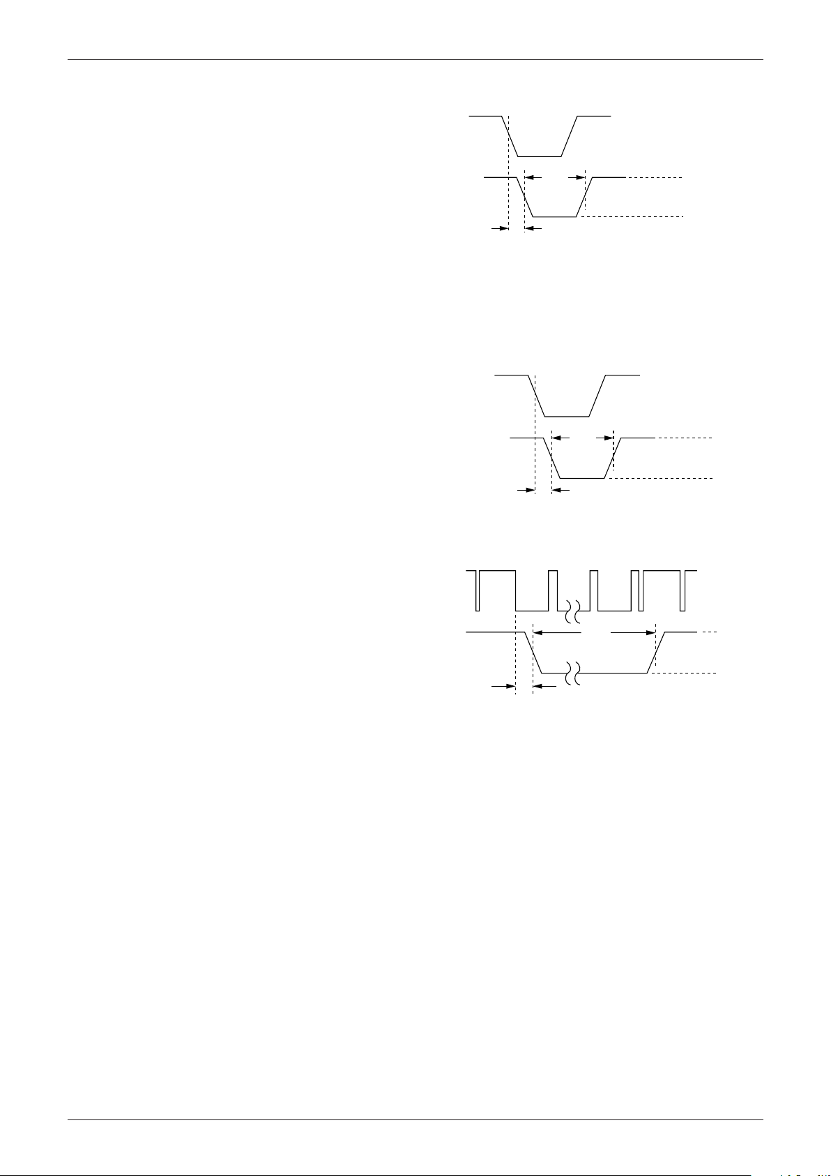
4 H. SYNC measurement
*
5 Measuring sync separation level
Gradually lower staircase wave signal sync tip level, and measure sync tip level when Pin 6 waveform
starts to change.
*
6 C. SYNC measurement
*
7 V. SYNC measurement
*
8 V. SYNC switching voltage measurement
Gradually change the DC voltage impressed on TP2, and measure TP2 voltage when TP3 output switches.
*
9 Sync discrimination switching voltage measurement
Gradually change the DC voltage impressed on TP5, and measure TP5 voltage when TP6 output switches.
Signal 1
TP1 waveform
t
w1
td1
VH1
V
L1
Input video signal
(Horizontal sync signal portion)
TP4 waveform
t
w2
td2
VH2
V
L2
Input video signal
(Vertical sync signal portion)
TP3 waveform
t
w3
td3
VH3
V
L3
Page 5
MITSUMI
No-adjustment Sync Separator + Sync Detector MM1067
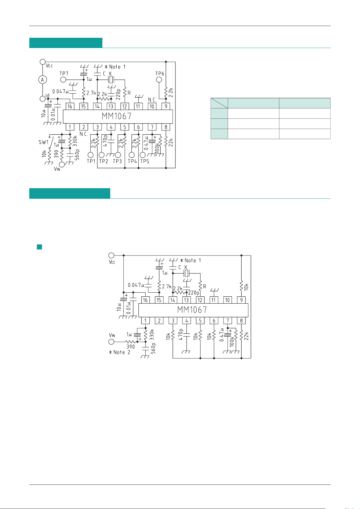
Measuring Circuit
Note : *1
NTSC PAL
X CSB503F2 CSB500F40
R 390Ω 220Ω
C 3300pF 4700pF
Application Circuits
There is a momentary phase lag in the H. SYNC output vertical feedback interval. When using this IC for OSD
timing, characters at the top of the screen may bend due to IC deviation. If this happens, change the
resistance between Pins 13 and 14 as shown, and the bending will improve by several H from the top edge of
the screen.
Application Circuit 1
Page 6
MITSUMI
No-adjustment Sync Separator + Sync Detector MM1067
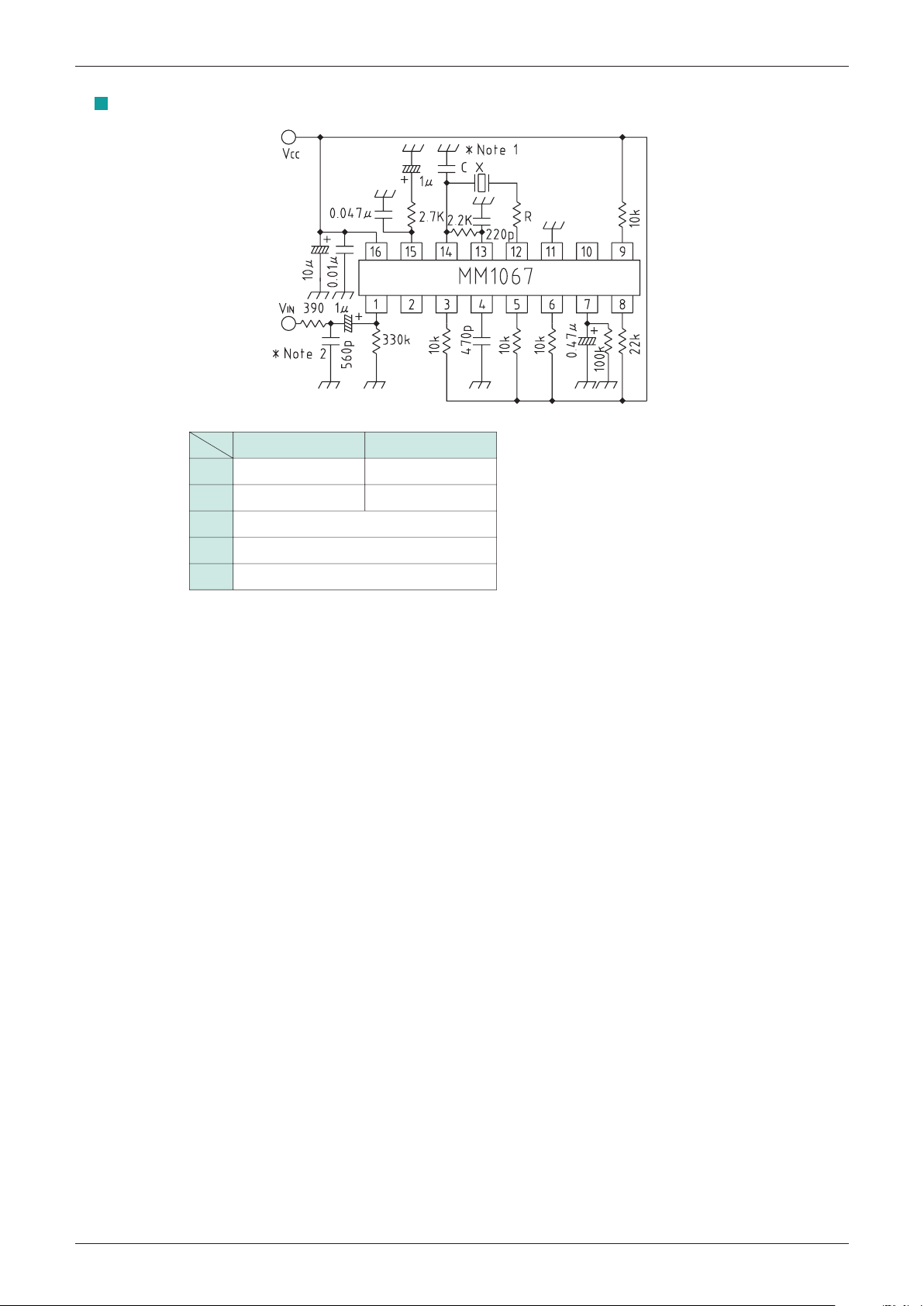
Note 1: 1. *1
NTSC PAL
X CSB503F2 CSB500F40
R1 1.5kΩ 1.8kΩ
R2 390Ω
C1 220pF
C2 3300pF
Note 2 :
1.
*
2 Input signal sync tip must be less than
1V for application circuit 1 Pin 1
external circuit.
2. The above 1. does not apply for
application circuit 2 Pin 1 external circuit.
Pin 1 is clamped at approximately 2.5V.
Application Circuit 2
2. Resistors R1 and R2 should have precision of ±1%.
3. Capacitors C1 and C2 should have precision of
±5% and temperature characteristic of CH class.
 Loading...