

Page 1
MITSUMI
1432
8567
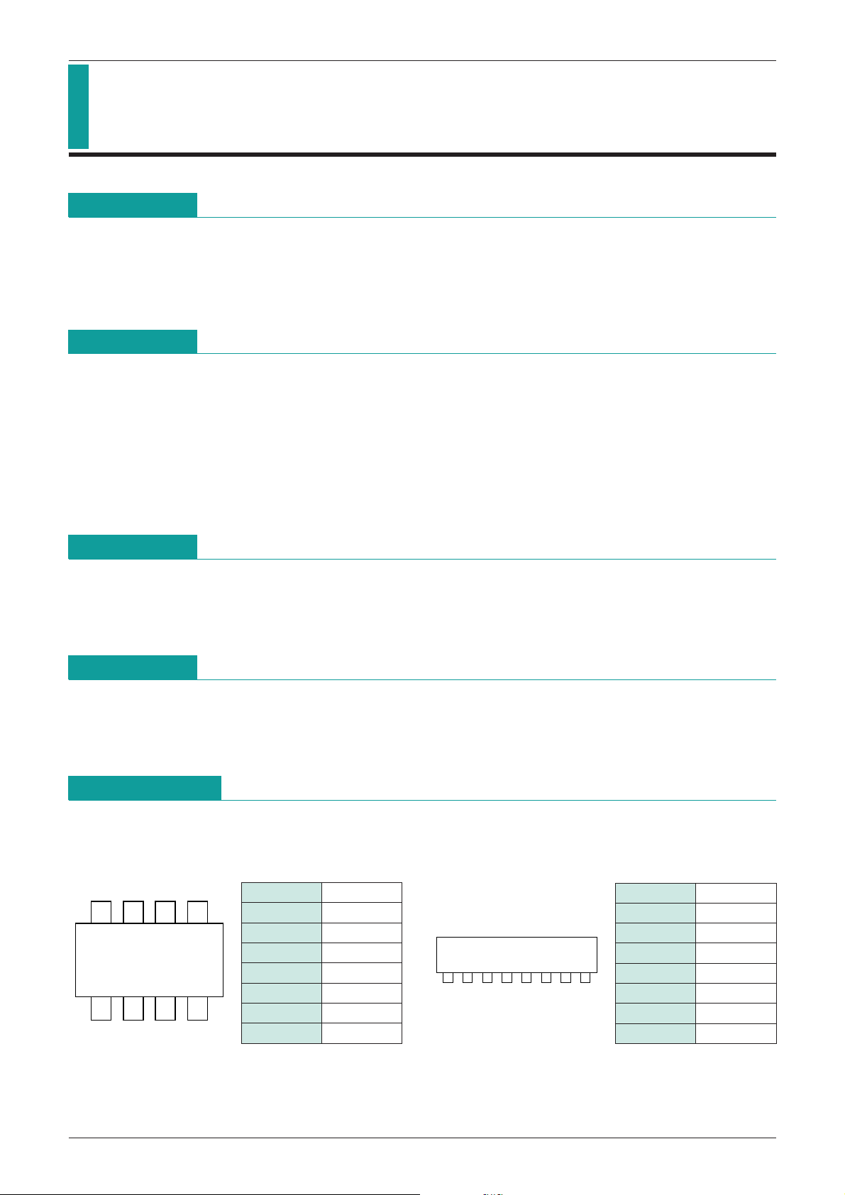
DIP-8B/SOP-8C
SIP-8A
13572468
System Reset (with built-in watchdog timer) MM1096
System Reset (with built-in watchdog timer)
Monolithic IC MM1096
Outline
This IC functions in a variety of CPU systems and other logic systems to generate a reset signal and reset the
system accurately during momentary interruption or lowering of power supply voltage.
It also has a built-in watchdog timer for operation diagnosis. This prevents the system from running wild by
generating an intermittent reset pulse during system mis-operation.
Features
1. Built-in watchdog timer
2. Low minimum operating voltage 130µA typ.
3. Low operating limit voltage V
4. Watchdog stop function (RCT pin)
5. Long clock monitoring time
T
PR (POWER ON) : TWD (clock monitoring)=1 : 5
6. Few external parts
CC=0.8V
Package
DIP-8B (MM1096AD, MM1096BD)
SOP-8C (MM1096AF, MM1096BF)
SIP-8A (MM1096AS, MM1096BS)
Applications
1. Reset circuits in microcomputers, CPUs and MPUs
2. Logic circuit reset circuits
3. Microcomputer system monitoring, etc.
Pin Assignment
1 TC
2 NC
3 CK
4 GND
5 V
6 RCT
7 V
8 RESET
CC
S
------------------------------------------------------
1 TC
2 NC
3 CK
4 GND
5 V
6 RCT
7 V
8 RESET
CC
S
------------------------------------------------------
Page 2
MITSUMI
Pin Description
System Reset (with built-in watchdog timer) MM1096
Pin No.
Pin name
TWD, TWR, TPR variable pins. TPR (mS) = 500 CT (µF)
1 TC
(T
WD, TWR and TPR times are determined TWD (mS) = 2500 CT (µF)
by the external capacitor.) T
2 N.C
3 CK
4 GND
5 V
6 RCT
7 V
---------------------------------------------------------------
8
RESET
Clock input pin, inputs clock from logic system
GND pin
CC
Voltage detection MM1096A 3.2V, MM1096B 4.2V
Watchdog timer stop pin Operation modes : Operation OPEN, Stop connect to GND
S
Detection voltage variable pin
Reset output pin (low output)
Absolute Maximum Ratings
Item Symbol Rating Units
Power supply voltage V
CK pin input voltage V
S pin input voltage VVS
V
Voltage applied to RCT pin V
Voltage applied to RESET
Allowable loss Pd 300 mW
Storage temperature T
----------------------------------------------------
CC max.
CK
RCT
pin VOH
STG
Function
-
-
0.3~VCC+0.3 (
-
0.3~VCC+0.3 (
-
0.3~VCC+0.3 (
-
0.3~VCC+0.3 (
-
WR (mS) = 100 CT (µF)
0.3~+10 V
<
+10) V
=
<
+10) V
=
<
+10) V
=
<
+10) V
=
40~+125
°
C
Recommended Operating Conditions
Item Symbol Rating Units
Power supply voltage V
----------------------------------------------------
RESET
sync current IOL 0~1.0 mA
Clock monitoring time setting T
Clock rise and fall times t
TC pin capacitance C
Operating temperature T
CC +2.2~+7.0 V
WD 0.1~1000 mS
FC, tRC <100 µS
T 0.0002~2 µF
OP
-
25~+75
°
C
Page 3
MITSUMI
System Reset (with built-in watchdog timer) MM1096
Electrical Characteristics (DC)
Item Symbol Measurement conditions Min. Typ. Max. Units
Consumption current
Detection voltage
Detection voltage temperature coefficient
Hysteresis voltage
CK input threshold V
CK input current
Output voltage MM1096A
(High) MM1096B V
Output voltage (Low)
R output sync current I
MM1096A
CC During watchdog timer operation
I
MM1096B 130 195
MM1096A
V
MM1096B 4.05 4.20 4.35
MM1096A
V
MM1096B 4.15 4.30 4.45
VS/ T ±0.01 %/°C
MM1096A
HYS
V
MM1096B 50 100 150
I
I
V
OL1 I =0.5mA, VS=0V 0.2 0.4
V
V
OL2 I =1.0mA, VS=0V 0.3 0.5
OL V =1.0V, VS=0V 1 2 mA
(Except where noted otherwise, MM1096A : V
CC
=3.6V, Ta=25°C, MM1096B : VCC=5.0V)
100 150
3.10 3.20 3.30
SL
VS=OPEN, VCC
3.15 3.25 3.35
SH
VS=OPEN, VCC
25 50 100
VSH-VSL, VCC
TH 0.8 1.2 2 V
IH A : VCK=3.6V, B : VCK=5.0V 0 1
IL VCK=0V
----------------------------------------------------
RESET
OH
I =1µA 3.0 3.4
S=OPEN 4.0 4.5
----------------------------------------------------
RESET
----------------------------------------------------
RESET
----------------------------------------------------
RESET
-
12-6
mV
-
2
µA
V
µA
V
V
T charge current
C
Minimum operating power
supply voltage to ensure RESET
---------------------------------------------------
I
CT1
I
CT2
VCCL 0.8 1.0 V
VTC=1.0V during watchdog timer operation-0.28-0.48-0.96 µA
VTC=1.0V during power ON reset operation-1.60-2.40-4.80 µA
----------------------------------------------------
RESET
V =0.4V
----------------------------------------------------
RESET
I =0.1mA
Page 4

MITSUMI
System Reset (with built-in watchdog timer) MM1096
Electrical Characteristics (DC)
(Except where noted otherwise, MM1096A : V
CC
=3.6V, Ta=25°C, MM1096B : Vcc=5.0V)
Item Symbol Measurement conditions Min. Typ. Max. Units
3.6V
2.8V
5.0V
CC input
V
pulse width
MM1096A 8
T
MM1096B 8
VCC
PI µS
VCC
4.0V
CK input pulse width T
CK input cycle T
CKW 3µS
CK 20 µS
CK or
Watchdog timer
T
monitoring time
1
*
WD CT=0.02µF 25 50 75 mS
Reset time for
T
watchdog timer
2
*
WR CT=0.02µF 1 2 3 mS
Reset hold time for
power supply rise *3
Output delay time from V
Output rise time
Output fall time
CC
*
5 tR RESET
*
5 tF RESET
*
TPR 51015 mS
4
TPD RESET
CT=0.02µF, VCC
--------------------------------------------------------------------------
pin, RL=10kΩ, CL=20pF 2 10 µS
--------------------------------------------------------------------------
pin, RL=10kΩ, CL=20pF 2.0 4.0 µS
--------------------------------------------------------------------------
pin, RL=10kΩ, CL=20pF 0.2 1.0 µS
Notes:
1 Monitoring time is the time from the last pulse (negative edge) of the timer clear clock pulse until reset
*
pulse output. In other words, reset output is output if a clock pulse is not input during this time.
2 Reset time means reset pulse width. However, this does not apply to power ON reset.
*
3 Reset hold time is the time from when VCC exceeds detection voltage (VSH) during power ON reset until
*
reset release (RESET
4 Output delay time is the time from when power supply voltage drops below detection voltage (VSL) until
*
5 Voltage range when measuring output rise and fall is 10~90%.
*
6 Watchdog timer monitoring time (TWD), watchdog timer reset time (TWR) and reset hold time (TPR) during
*
-----------------------------------------------
reset (RESET
power supply rise can be changed by varying C
-----------------------------------------------
output high).
output low).
T capacitance. The times are expressed by the following
formulae.
PR (mS)
T
T
WD (mS)
T
WR (mS)
.
=.500 CT (µF)
.
=.2500 CT (µF)
.
=.100 CT (µF)
Example : When C
.
T
=.10mS
PR
.
T
WD
=.50mS
.
T
WR
=.2mS
T=0.02µF
Page 5

MITSUMI
System Reset (with built-in watchdog timer) MM1096
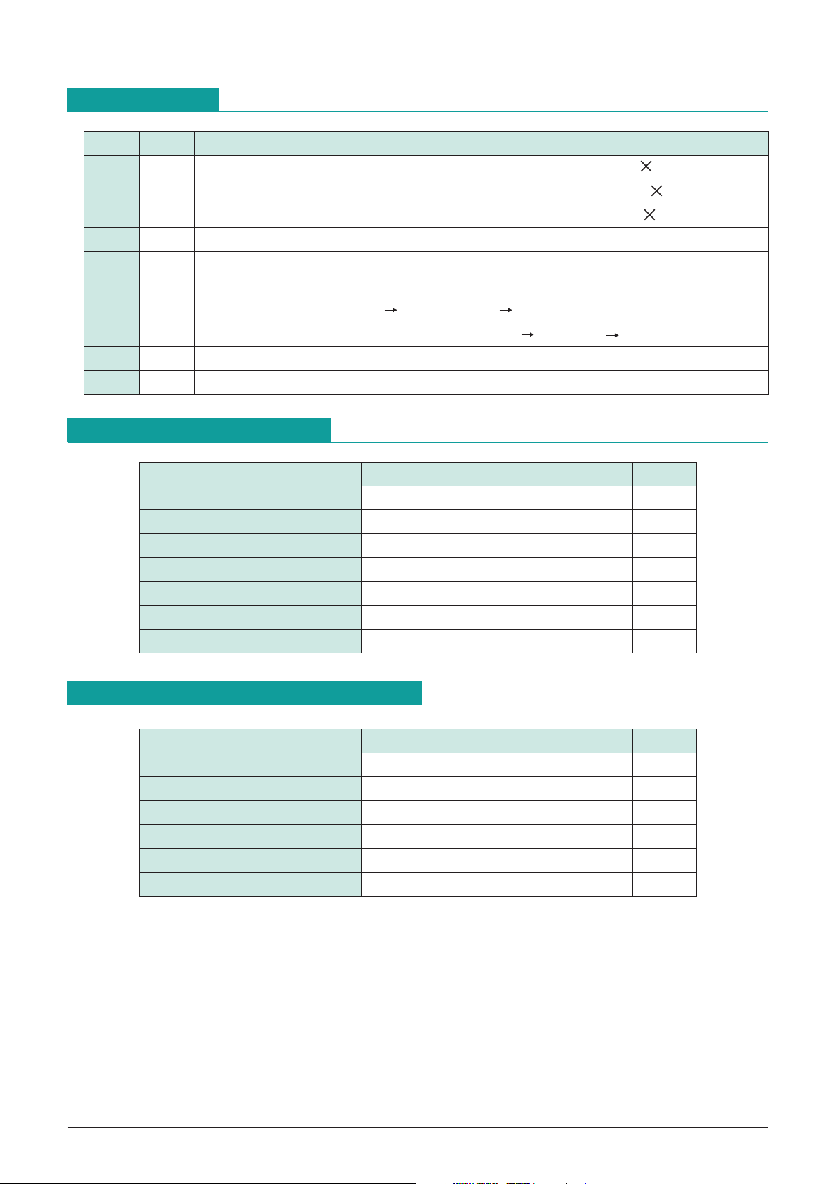
Measuring Circuits
Measuring Circuit 1 (DC) Measuring Circuit 2 (AC)
Measuring Circuit 1
Item
Consumption current I
Detection voltage
CK input threshold V
CK input current
Symbol
SW & Power Supply Table
-----------------------------------------------
1V
RESET
-
-
-
-
-
-
SW1 SW2 SW3 SW4 SW5 SW6 SW7 VCC VCK VCT I VM, IM Notes
CC OFF OFF OFF ON ON ON A 3.6V 3.6V 0V
SL OFF OFF ON ON ON ON A
V
SH OFF OFF ON ON ON ON A
V
TH OFF OFF OFF ON ON ON A 3.6V
IH OFF OFF OFF ON ON ON A 3.6V 3.6V 0V
I
3.6V 3V
3V 3.6V
0V 2V
0V 2V
0V 3V
IIL OFF OFF OFF ON ON ON A 3.6V 0V 0V
Output voltage (High) VOH ON OFF ON ON ON ON A 3.6V 3.6V 2V-1µA VO1
OL1 ON ON ON ON ON ON A 3.6V 3.6V 2V 0.5mA VO1
Output voltage (Low)
Output sink current I
T charge current 1 ITC1 OFF OFF OFF ON ON OFF A 3.6V
C
CT charge current 2 ITC2 OFF OFF OFF ON ON OFF A 3.6V
Minimum operating power
supply voltage to ensure RESET
Measuring Circuit 2
Item
CC input pulse width TP1C B
V
CK input pulse width T
CK input cycle T
Watchdog timer
monitoring time CRT2
Reset time
for watchdog timer CRT2
Reset hold time for
power supply rise CRT2
Output delay time
CC
from V
Output rise time T
Output fall time T
V
V
OL2 ON ON ON ON ON ON A 3.6V 3.6V 2V 1.0mA VO1
OL1 OFF ON ON ON ON ON B 3.6V 3.6V 2V
VCCL ON OFF ON ON ON ON A
------------------------------------------------------
SW & Power Supply Table
Symbol
SW1 SW2 VCCA VCC VCKA VCK CRT Notes
CKW AB
CK AB
T
WD AA
T
WR AA
PR
B A
T
A
TPD CA
R AA
F AA
3.6V
2.8V
3.6V
0V
T1
-
-
-
-
-
-
-
1.4V
-0V
1.4V
3.6V
0V
1.4V
3.6V
0V
3.6V
3.6V
3.6V
--
3.6V
3.6V
0V 2V
-
-
0V 0V
T2 T3
T2
or
T2 T3
-
-
-
-
-
1V
IV
T2
-
-
-
-
-
-
3.6V
3.6V
3.6V
0V CRT1
3.6V CRT1
3.6V CRT1
ICC
VO1, CRT1
VO1, CRT1
ICK, VCK
ICK
ICK
IO1VO=1V
ITC
ITC
VO1, VCC
CRT1
CRT2
CRT1
CRT2
CRT1
CRT2
CRT1
CRT1
CRT1
T1=8µS
T2=3µS
T3=20µS
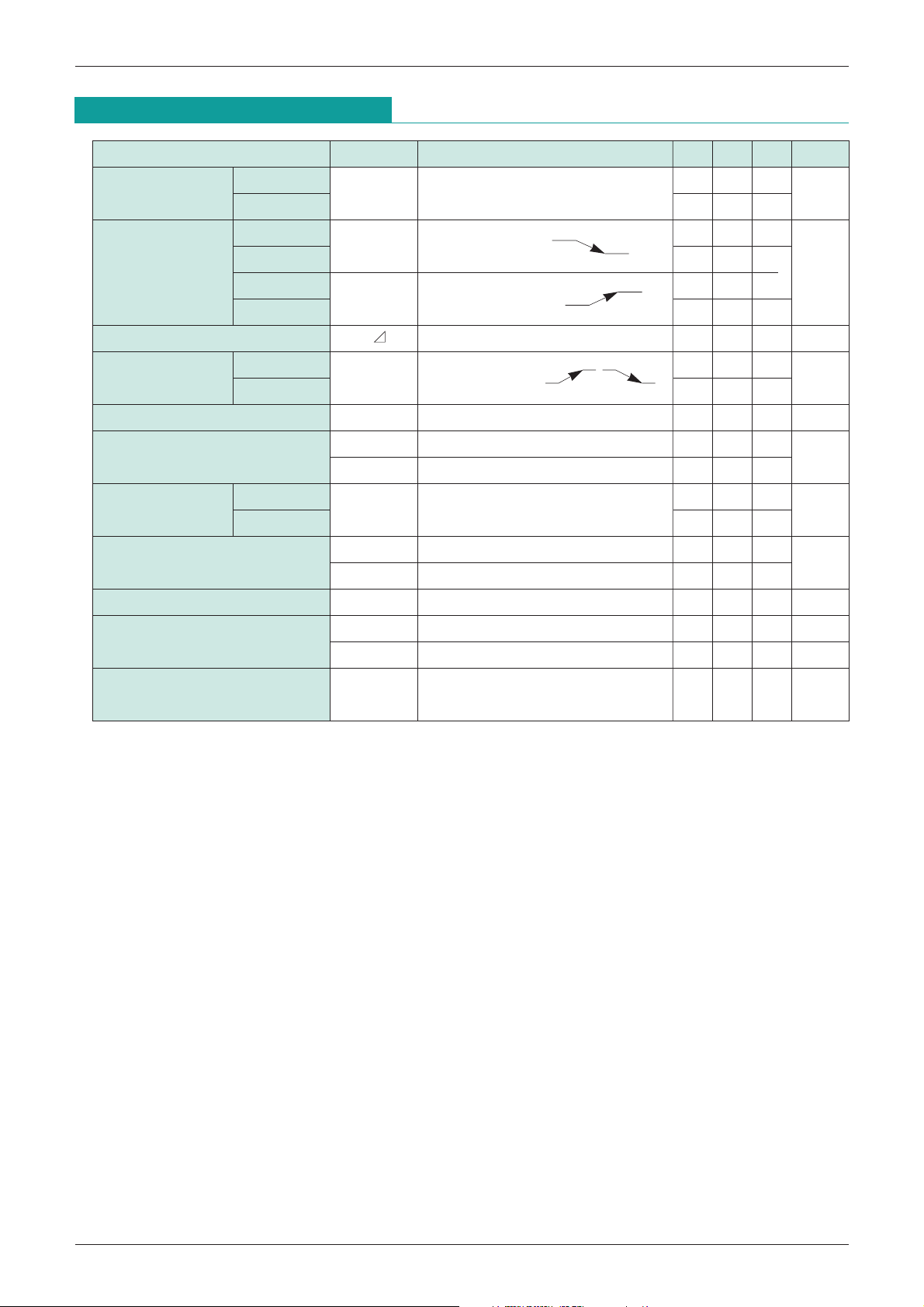
Page 6

MITSUMI
VCC
CK
CT
RESET
VSL
VSH
TCK
TPR
TWD
TWR
TPR
21
3 4
5 5 6
7 8 9
10
11
12
Block Diagram
System Reset (with built-in watchdog timer) MM1096
RA RB
MM1096A
MM1096B
~
~
-
305k
350k
~
~
-
195k
150k
Note 1: CP=0.1µF approx.
Note 2: C=1000pF
Note 3: The watchdog timer
can be stopped by
connecting the RCT
pin to GND. Then it
functions as a voltage
detection circuit.)
Timing Chart
Page 7

MITSUMI
System Reset (with built-in watchdog timer) MM1096
Description of Operation
-------------------------------------------------
1. RESET
Approximately 1µA (V
2. Capacitor CT charging starts when VCC rises to VSH (MM1096A .=.3.25V, MM1096B .=.4.3V). Output is in
reset state at this time.
3. Output reset is released (RESET
discharge (the time from when C
drops to a certain threshold value 2 (.=. 0.2V).
Reset hold time : T
T
C
Clock input to the CK pin during C
4. If a clock is input (negative edge trigger) to the CK pin during C
discharge.
5. Discharge switches to charging when C
5 are repeated while a normal clock is input from the logic system.
6. Output goes to reset state (RESET
threshold value (.=.1.4V).
The formula for C
T
7. Watchdog timer reset time T
(.=.0.2V). The formula is as follows.
T
After reset OFF threshold value is reached, output reset is released and C
steps 4 and 5 are repeated if a normal clock is input, and when the clock ceases, 6 and 7 are repeated.
8. Reset is output when V
simultaneously.
9. C
When V
dropping below VSL until it rises to VSH is longer than the Vcc input pulse width standard value TPI.
10.Output reset is released after V
8~10 are repeated when V
11.When power is OFF, reset is output if V
12.When V
goes low when VCC rises to approximately 0.8V.
CC=0.8V) of pull up current is output from RESET
-----------------------------------------------
PR (mS)
T charging starts again after reset release, and watchdog timer operation begins.
WD (mS)
WR (mS)
T charging starts when VCC rises to VSH.
.
=. 500 CT (µF)
.
=.2500 CT (µF)
.
=.100 CT (µF)
CC drops momentarily, CT charging begins after the charge is first discharged, if the time from VCC
CC drops to 0V, reset output is held until VCC reaches 0.8V.
PR is as follows.
T charging time (TWD : watchdog timer monitoring time) until reset is output is as follows.
CC drops to VSL (MM1096A
goes high) after a certain time (TPR), from when CT starts charging until
T voltage reaches a certain threshold value 1 (
T charging will cause mis-operation.
T voltage drops to a certain threshold value (
-----------------------------------------------
CC goes below VSL.
goes low) when the clock ceases and CT voltage reaches reset ON
WR is the discharge time until CT voltage drops to reset OFF threshold value
.
=.3.2V, MM1096B .=.4.2V). CT is charged
CC goes above VSH and after TPR, and the watchdog timer starts. Thereafter,
CC goes below VSL.
-------------------------------------------------
.
=. 1.4V) until CT voltage
T charging, C switches from charging to
.
=.0.2V). Steps 4 and
T starts charging. Thereafter,
 Loading...