

Page 1
MITSUMI
Compander IC MM1077
Compander IC
Monolithic IC MM1077
Features
This IC was developed for use in cordless telephone equipment. It is a compander IC incorporating
compressor/expander circuits for a significant noise reduction effect without complicated external circuitry.
On the transmission side, the dynamic range of audio signals is compressed by the compressor circuit; on the
receiving side, the expander expands the signals. As a result the dynamic range over the transmission
channel is reduced logarithmically by one-half.
1. Can be driven at low voltages (down to 2.0V)
2. Internal mute function
3. Internal limiter (IDC) function
4. Compressor input can be switched between MIC and LINE
5. Internal standby function
6. Data input, output pins
7. Independent mute circuit
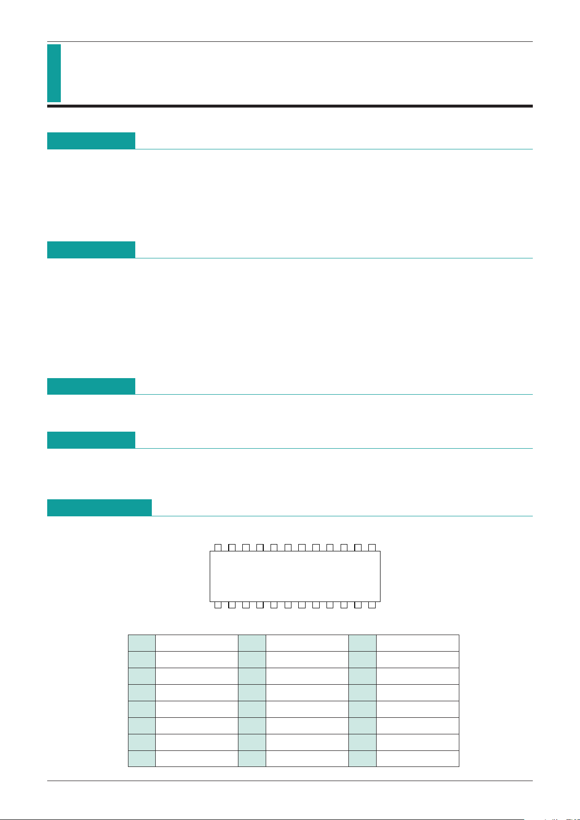
Package
SSOP-24A (MM1077XF)
Pin Assignment
SSOP-24A
136924587101211
24 20 1723 21 19 18 1622 131415
Applications
1. Cordless telephones
2. Various mobile communication devices
1 C.Vref 9 DATA. IN 17 E.RECT
2 C.IN1 10 C.CONT 18 E.OUT
3 C.IN2 11 N.C 19 E.RIN
4 C.IN
-
12 GND 20 A.OUT
5 C.RECT 13 STANDBY SW 21 A.IN
-
6 C.RIN 14 C.IN SW 22 A.IN+
7 C.FB 15 C.MUTE SW 23 E.Vref
8 C.NF 16 E.MUTE SW 24 Vcc
Outline
Page 2
MITSUMI
Compander IC MM1077
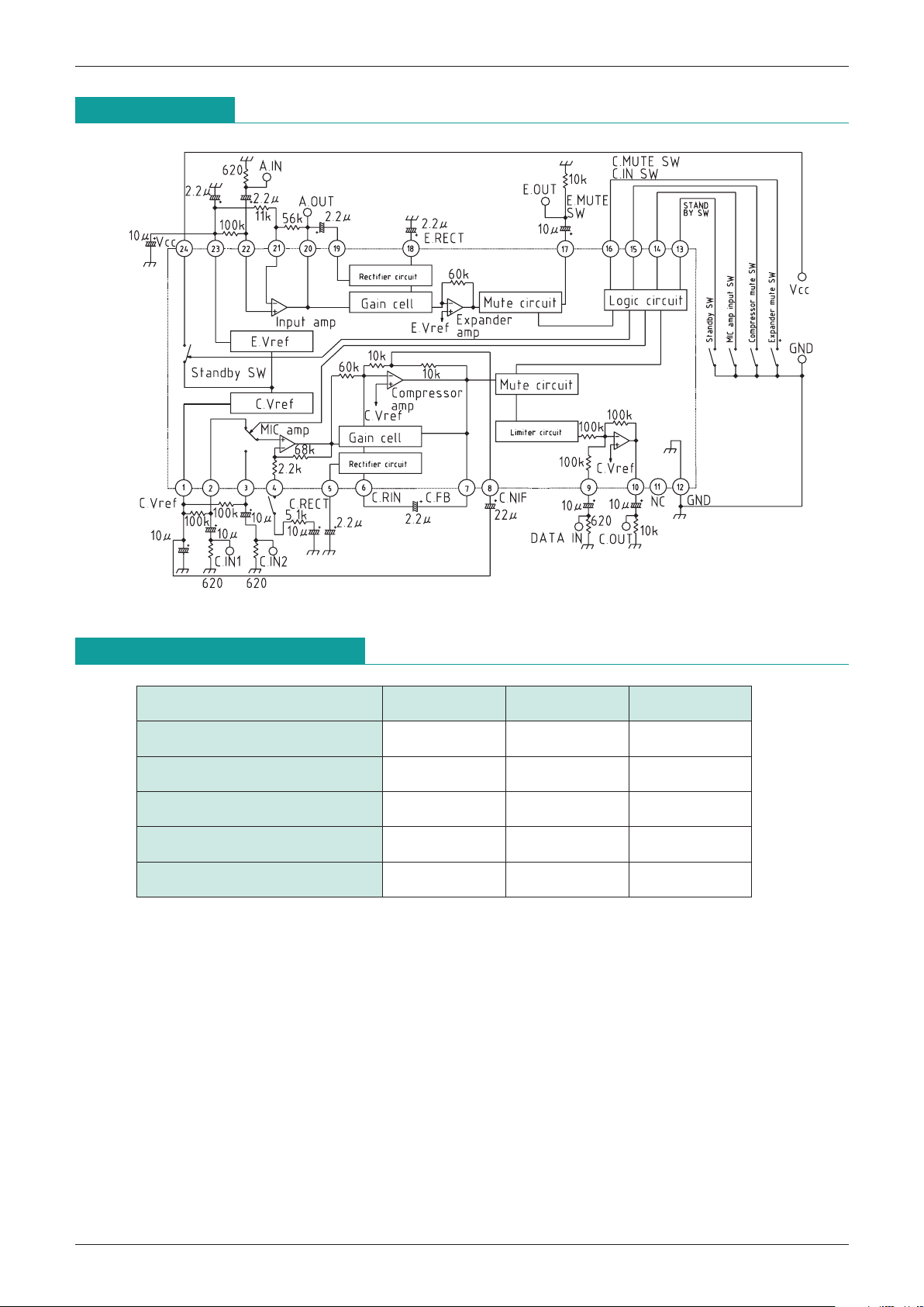
Block Diagram
Absolute Maximum Ratings
(Ta=25°C)
Item Symbol Ratings Units
Storage temperature T
STG
-
40~+125
°
C
Operating temperature T
OPR
-
10~+70
°
C
Power supply voltage V
CC max.
-
0.3~+8 V
Allowable loss Pd 650 mW
Operating voltage +2.0~+7 V
Page 3
MITSUMI
Compander IC MM1077
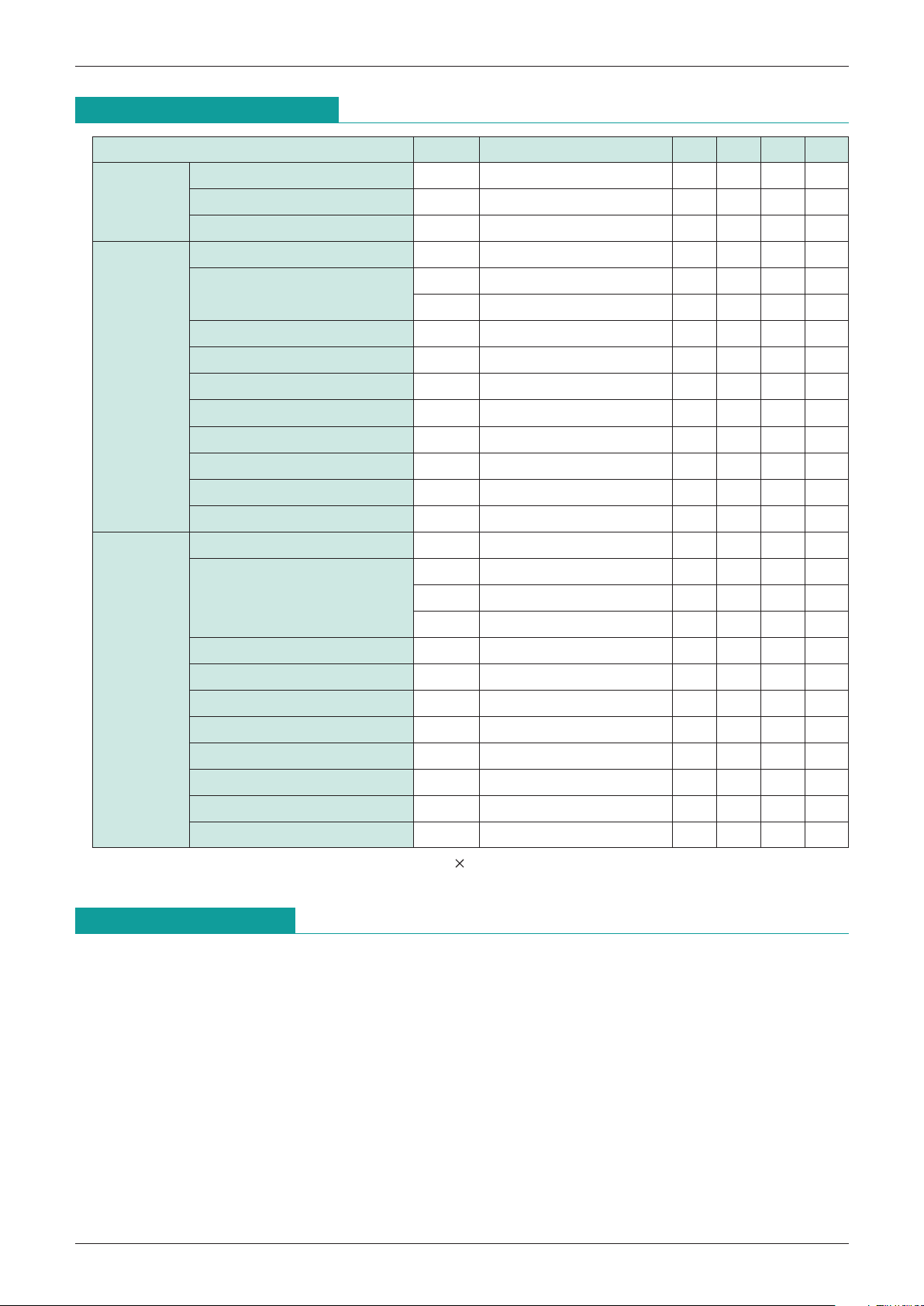
Electrical Characteristics
(Except where noted otherwise, Ta=25°C, VCC=3V, fin=1kHz)
Function Description
Item Symbol Measurement conditions Min. Typ. Max. Units
Consumption current I
CC No signal 4.0 6.0 mA
Standby current consumption Iscc 0 10 µA
Threshold voltage Vth 0.40 0.65 0.80 V
Input reference level V
INc Voc=100mVrms, VIN=0dB 8.0 13.5 18.0
mVrms
Gain error
*
Gc1 VIN=-20dB
-
0.5 0 0.5 dB
Gc2 V
IN=
-
40dB
-
1.0 0 1.0 dB
Distortion THDc V
IN=0dB 0.3 1.0 %
Output noise voltage Vnc No signal (CCITT) 2.5 5.0
mVrms
Mute attenuation Attc VIN=0dB, C.MUTE SW : ON 40 50 dB
Limit voltage Vlimc THD=10% 700 800 900
mV
p-p
DATA pin voltage gain GDATA C. MUTE SW : ON, VIN=0dB-0.5 0 0.5 dB
DATA pin maximum output VD max.
C.MUTE SW : ON, THD=10%
800 900
mVrms
Crosstalk CTc EXPVIN=0dB 28 33 dB
Ripple rejection ratio RRc V
R=100mVrms, fR=1kHz 18 23 dB
Input reference level V
INe Voe=100mVrms, VIN=0dB 25 35 50
mVrms
Ge1 VIN=-10dB
-
0.5 0 0.5 dB
Gain error difference
*
Ge2 VIN=-20dB
-
1.0 0 1.0 dB
Ge3 V
IN=
-
30dB
-
1.5 0 1.5 dB
Distortion THDe V
IN=0dB 0.15 1.0 %
Maximum output voltage
Ve max.
THD=10% 600 800
mVrms
Output noise voltage Vne No signal (CCITT) 20 40
µVrms
Mute attenuation Atte VIN=0dB, C. MUTE SW : ON 60 70 dB
Input amp voltage gain GI V
IN=0dB 14.6 15.6 16.6 dB
Input amp maximum output
Veo max.
THD=10% 0.90 1.10 Vrms
Crosstalk CTe COMPV
IN=0dB 60 75 dB
Ripple rejection ratio RRe V
R=100mVrms, fR=1kHz 50 60 dB
Compressor
unit
Expander
unit
1. Compressor unit
The compressor unit consists of the mike amp, compressor, limiter circuit, data amp, and mute circuit.
The mike amp gain can be adjusted through an external resistance, and so the mike amp can be
connected directly to a microphone. An internal limiter circuit to prevent overmodulation as well as a data
amp (0dB amp) enabling transmission of data signals without compression are also provided. Switching
between audio signals and data signals is possible using the compressor mute switch.
2. Expander unit
The expander unit consists of an input amp, expander, and mute circuit.
The input amp makes available all input and output signals at pins, and so can be used freely as an
amplifier, filter amp, or data amp. When used as a data amp, the expander mute switch can be set so that
the expander output is nearly silent.
*
Gain error difference = (VOUT (dBv)+20dB) -VIN (dB) G (dB)
G : COMP=0.5, EXP=2
Page 4

MITSUMI
Compander IC MM1077
About Application Circuits
The compressor unit mike amp is exposed to circuits outside the IC via positive and negative input pins.
The positive input pin is connected to C.Vref by a bias resistance of 100kΩ, so that no external bias is
needed.
When pin 4 is open the gain is lowest, and an input voltage of approx. 13.5Vrms is the reference level.
When the external resistance is 0Ω, the gain is maximum. The internal configuration appears in Fig. 1.
1. Mike amp
The product of the external capacitance and the internal resistance (10kΩ) determines the time constants
for the attack and release times.
2. Rectifier circuit unit (rectifier)
The compressor amp requires that the DC gain be unity and the AC gain be infinite. In order to satisfy this
requirement, AC feedback is eliminated and only DC feedback is used. In order that only DC feedback be
present, a capacitor to eliminate AC components is connected to pin 8. The cutoff frequency is determined
by the product with the internal resistance (100kΩ).
3. Compressor amp
Page 5

MITSUMI
Compander IC MM1077
The data amp uses an inverting amp. The internal input resistance is 100kΩ, and the DC bias voltage is
1.3V. The compressor mute switch at pin 15 is used to switch between data signals and audio signals.
4. Compressor data amp
The positive and negative input pins and the output pin are exposed to circuitry outside the IC. The
expander input amp can be used as a signal amplifier, a buffer amplifier, and a filter amp. By taking the
signal from this amp's output pin, the data signal can be obtained without passing through the expander. If
the expander mute switch is turned on, this signal can be prevented from appearing in the expander output.
5. Expander input amp
The internal equivalent circuit for each of these switches appears in Fig. 6.
6. Mike amp input switch and mute switches
The internal equivalent circuit for the standby switch appears in Fig. 7.
7. Standby switch
Page 6

MITSUMI
Compander IC MM1077
Measuring Circuit
(Except where noted otherwise, fIN=1kHz)
1. Consumption current
2. Threshold voltage
3. Input reference level
4. Gain error difference
Gain error difference= (V
OUT
(dBv) -20dB) -VIN(dB) G
(G=COMP=0.5, EXP=2)
Gain error difference (1) Gc1=
-
20dB, Ge1=-10dB
Gain error difference (2) Gc2=
-
40dB, Ge2=-20dB
Gain error difference (3) Ge3=
-
30dB
6. Limit voltage
7. Maximum output voltage
8. DATA pin/Input amp voltage gain
5. Distortion
Page 7

MITSUMI
Compander IC MM1077
9. DATA pin/Input amp maximum output
10. Crosstalk
11. Ripple rejection
12. Output noise voltage
13. Mute attenuation
 Loading...