

Page 1
MITSUMI
HBS-Compatible Driver and Receiver MM1007
HBS-Compatible Driver and Receiver
Monolithic IC MM1007
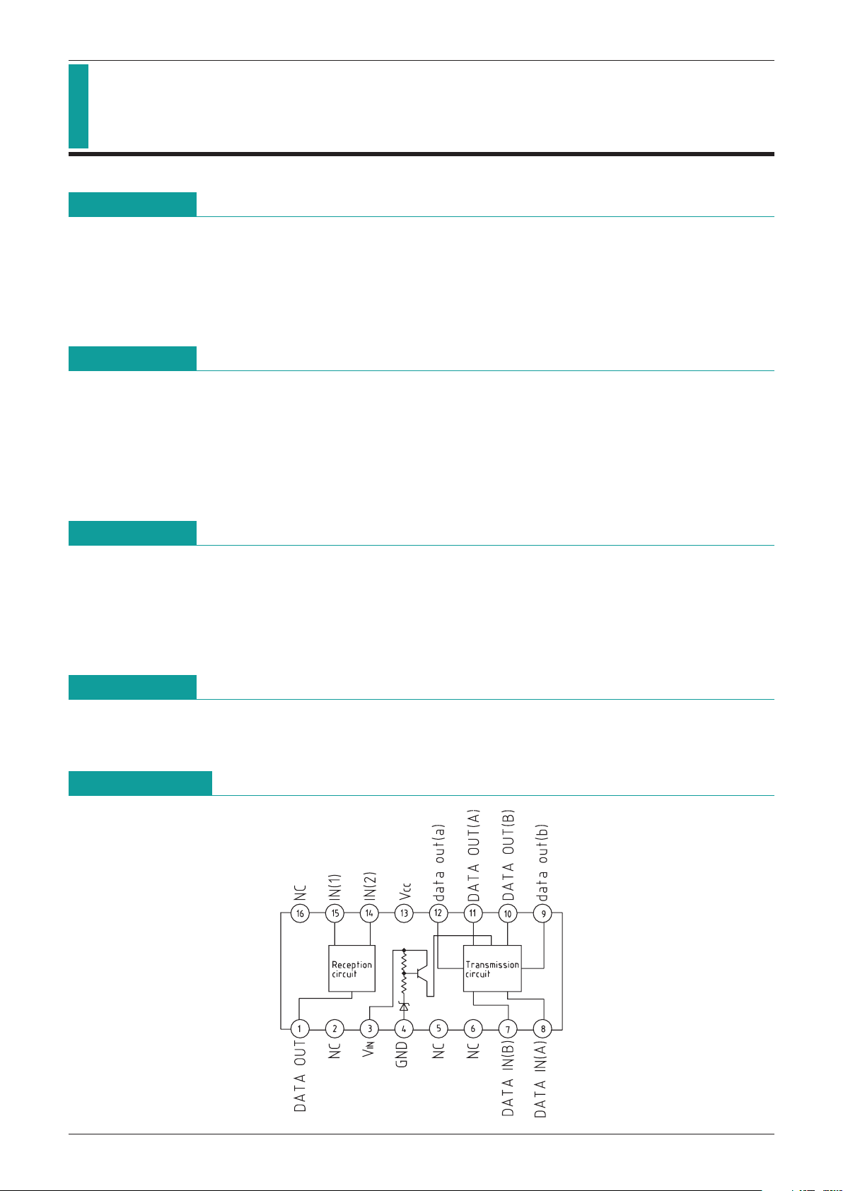
This IC conforms to the HBS (Home Bus) specification (Electronic Industries Association of Japan), and has
functions for the reception and transmission of data. AMI is adopted for the waveforms of signals handled by
the transmission and reception units, designed for connection to twisted-pair lines. Telephone equipment,
security devices, audio or video equipment, air-conditioning equipment, and a wide range of other devices
can be connected to a bus line to enable mutual communications.
Features
1. Compact design
2. High reliability
3. Replaces pulse transformers
4. Low cost
5. Easy circuit design
6. Few external components
Applications
1. Telephony equipment
2. Security equipment
3. Audio and video devices
4. Air-conditioning equipment
5. Wide range of other equipment and devices
Package
DIP-16A (MM1007XD)
SOP-16A (MM1007XF)
Block Diagram
Outline
Page 2
MITSUMI
HBS-Compatible Driver and Receiver MM1007
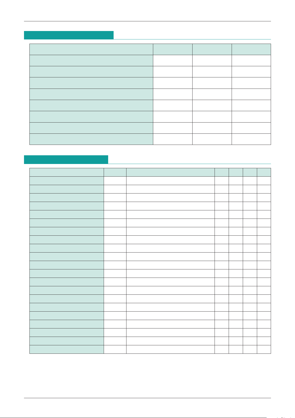
Absolute Maximun Ratings
(Ta=25°C)
Item Symbol Ratings Units
Operating temperature T
STG
-
40~+125
°
C
Storage temperature T
OPR
-
20~+175
°
C
Bias voltage V
B max.
-
0.3~+41 V
Power voltage V
CC max.
-
0.3~+7 V
Allowable loss Pd 450 mW
Recommended power supply voltage range V
CCOP 4.75~5.25 V
Recommended bias voltage range V
BOP 8~40 V
Operating power supply voltage range V
CCOP2 4.5~5.5 V
Electrical Characteristics
(Except where noted therwise, Ta=25
°
C, VCC=5V, VB=30V, Ftransmit=10kHz (DUTY=50%))
Item Symbol Measurement conditions Min. Typ. Max. Units
Power supply current I
CCO No signal (7-8PIN=H) 7 10 mA
Power supply current I
CCON In transmission FL=10k, RL=36Ω 65 75 mA
Bias current pin 3 I
BO No signal (7-8PIN=H) 220 350 µA
Bias current pin 3 I
BON In transmission FL=10k, RL=36Ω 1.5 2.2 mA
Transmission output voltage V
TO Both pins 10 and 11 3.8 4.2 4.6 VP-P
Transmission waveform symmetry
VTR VTO1/VTO2 0.75 1.0 1.25
Reception sensitivity V
RS 0.65 0.75 0.85 VP-P
Noise resistance VRN Level at which no errors are output 0.55 VP
-
P
Input impedance RIN Both pins 14 and 15 25 36 46 kΩ
Transmission delay time 1 T
d1 cf. transmit/receive waveform diagrams 0.2 µS
Transmission delay time 2 T
d2 cf. transmit/receive waveform diagrams 0.4 µS
Transmission delay time 3 T
d3 cf. transmit/receive waveform diagrams 0.7 µS
Transmission delay time 4 T
d4 cf. transmit/receive waveform diagrams 1.0 µS
Reception output H voltage V
ROH 4.5 VCC V
Reception output L voltage V
ROL 0.5 V
Transmission waveform LOSS1 V
TLS1 H level input voltage 4.5 V
Transmission waveform LOSS2 V
TLS2 L level input voltage 4.5 V
H level input voltage V
LIH 2.4 V
L level input voltage V
LIL 0.8 V
H level input current I
LIH VIN=2.4V 10 µA
L level input current I
LIL VIN=0.4V
-
300 µA
When a negative voltage is applied to pins 10 and 11, there should be no abnormal operation of internal
circuits between 0 and 6V. However, if a negative voltage exceeding
-
6V is applied, thyristor operation may
result, so it is recommended that an external clamping diode be added.
Page 3
MITSUMI
HBS-Compatible Driver and Receiver MM1007
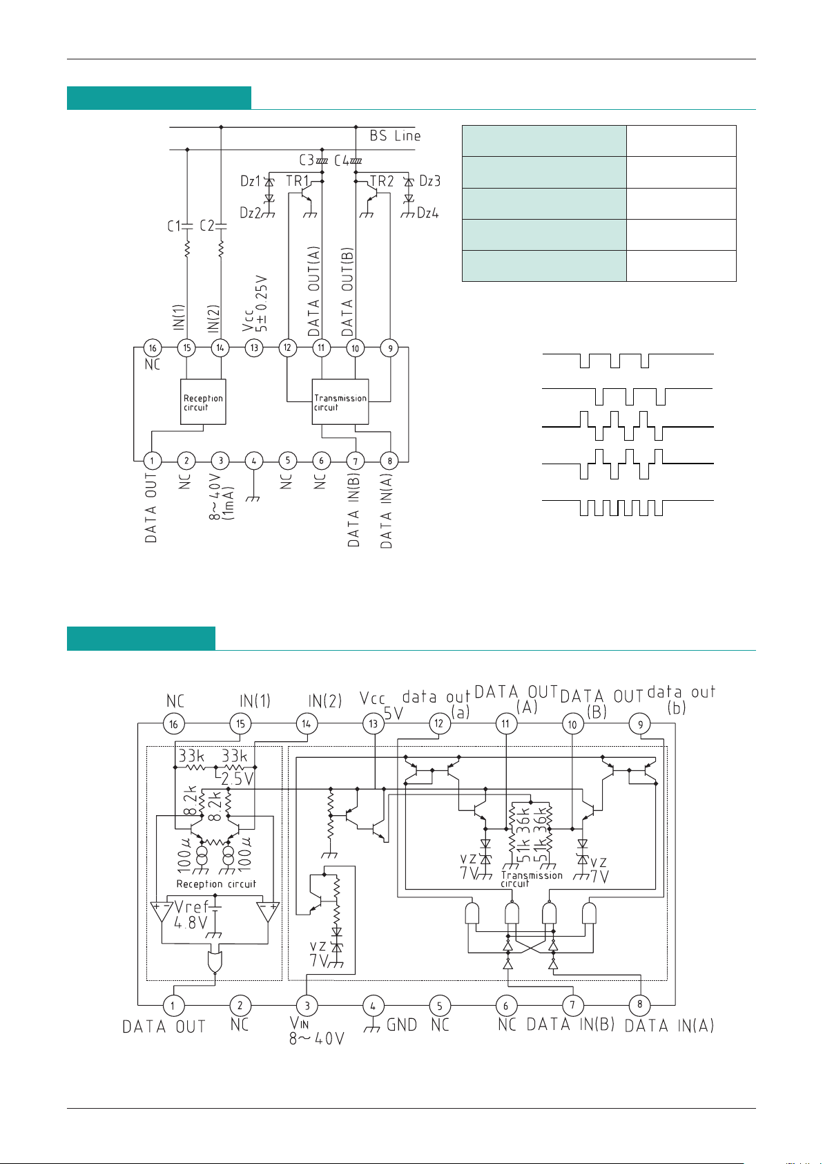
Application Circuits
DATA IN A
DATA IN B
Transmission DATA OUT A
Transmission DATA OUT B
Reception DATA OUT
TR1, TR2 2SC2001
C1, C2 0.022µF
R1, R2 33kΩ
C3, C4 10µf
D
Z1, DZ2, DZ3, DZ4 VZ=5.6V
Circuit Diagram
Page 4
MITSUMI
HBS-Compatible Driver and Receiver MM1007
MM1007
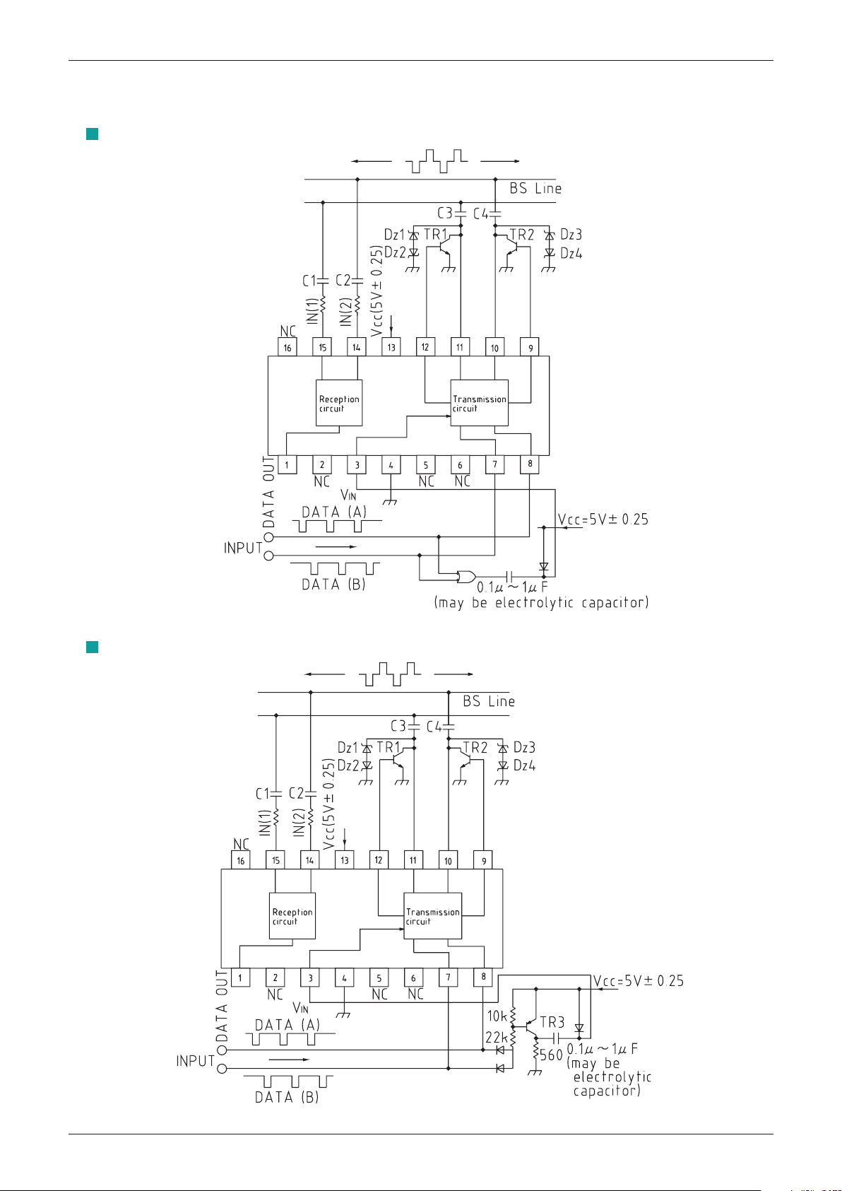
When used with a single +5V power supply
APPLICATION 1
APPLICATION 2
 Loading...