

Page 1
MITSUMI
System Reset (with built-in watchdog timer) MM1035
System Reset (with built-in watchdog timer)
Monolithic IC MM1035
Outline
This IC functions in a variety of CPU systems and other logic systems to generate a reset signal and reset the
system accurately during momentary interruption or lowering of power supply voltage.
It also has a built-in watchdog timer for operation diagnosis. This prevents the system from running wild by
generating an intermittent reset pulse during system mis-operation.
Features
1. Built-in watchdog timer
2. Low minimum operating voltage V
3. Both positive and negative logic reset output can be extracted
4. Accurate detection of drop in power supply voltage
5. Detection voltage has hysteresis
6. Few external parts 1 capacitor
CC=0.8V typ.
Package
DIP-8A (MM1035XD)
SOP-8A (MM1035XF)
Applications
Microcomputers
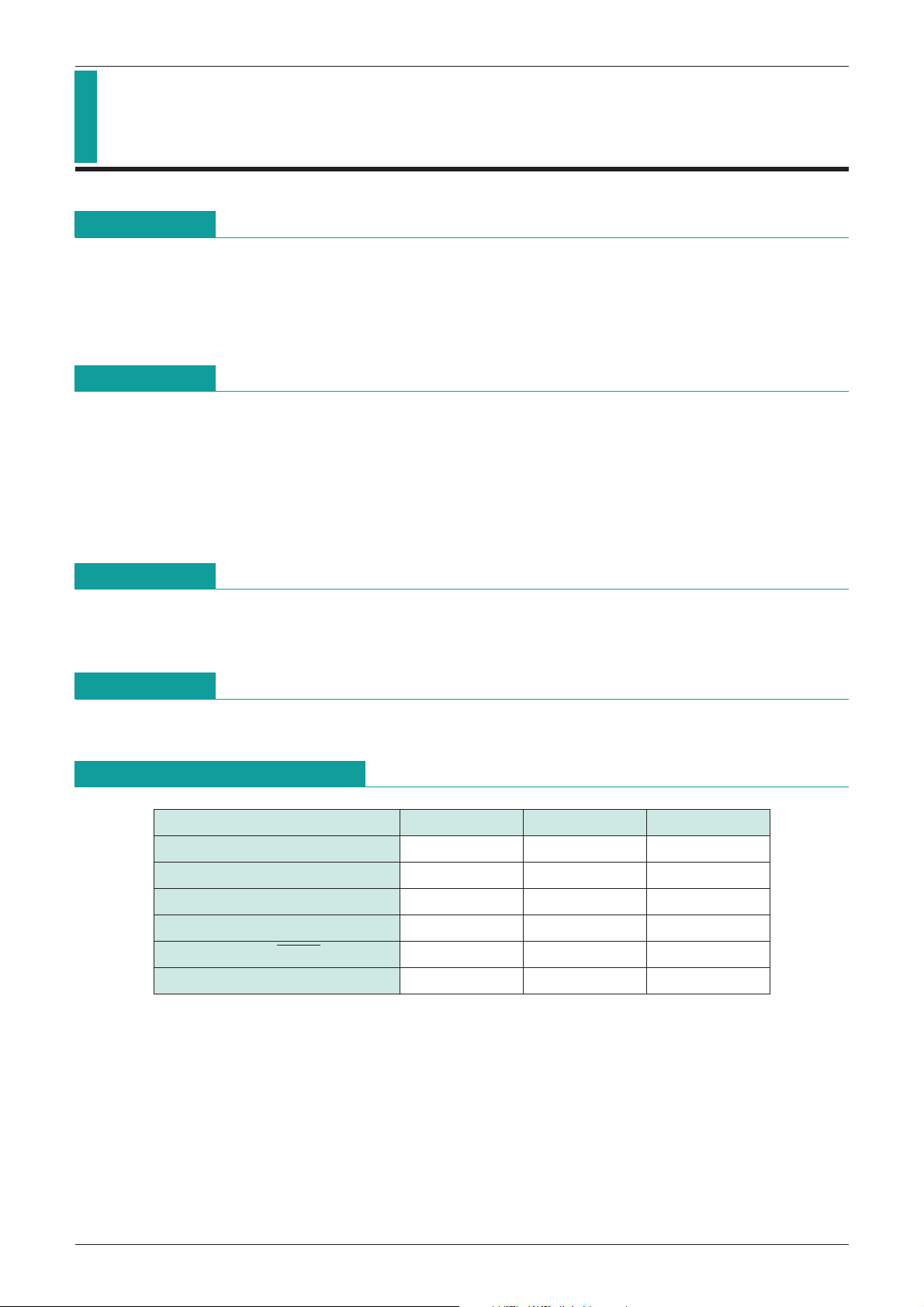
Absolute Maximum Ratings
Item Symbol Rating Units
Storage temperature T
Operating temperature T
Power supply voltage V
Voltage applied to VS & CK pins V
Voltage applied to RESET, RESET pin
Allowable loss Pd 400 mW
(Ta=25°C)
STG
OPR
CC max.
VS & VCK
VOH
-
40~+125
-
20~+70
-
0.3~+10 V
-
0.3~+10 V
-
0.3~+10 V
°
C
°
C
Page 2
MITSUMI
System Reset (with built-in watchdog timer) MM1035
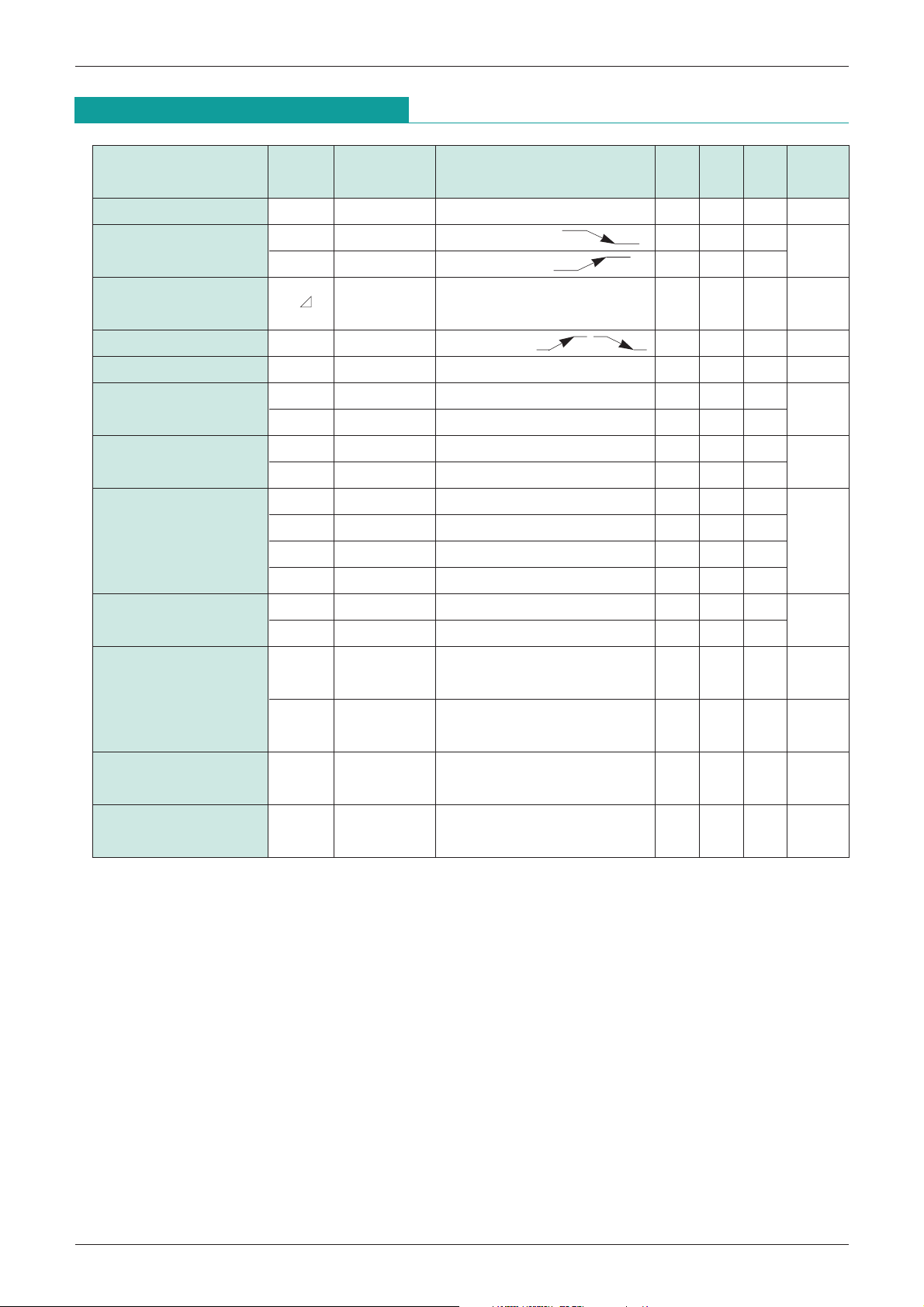
Electrical Characteristics 1 (DC)
Item Symbol
Consumption current I
Detection voltage
Detection voltage
temperature coefficient
Hysteresis voltage V
CK input threshold V
CK input current
Output voltage (High)
Output voltage (Low)
V
S/ T 1 ±0.01 %/°C
V
V
V
V
V
Measurement
circuit
CC 1
V
SL 1 4.05 4.20 4.35
SH 1 4.15 4.30 4.45
V
HYS 1 50 100 150 mV
TH 1 0.8 1.2 2 V
I
IH 1VCK=5V 0 1
IL 1VCK=0V
I
OH11 I=
OH21 IRESET=
OL1 1 I =3mA, VS=0V 0.2 0.4
OL2 1 I =10mA, VS=0V 0.3 0.5
OL31 IRESET=0.5mA, VS=OPEN 0.2 0.4
(Except where noted otherwise, Ta=25°C, VCC=5V, measurement circuit 1)
Measurement conditions Min. Typ. Max. Units
During watchdog timer operation
VS=OPEN, VCC
0.7 1.0 mA
V
VS=OPEN, VCC
VSH-VSL, VCC
µA
-
-----------------------------------------
RESET
20-10
-
5µA, VS=OPEN 4.5 4.8
-
3
V
-
5µA, VS=0V 4.5 4.8
-----------------------------------------
RESET
-----------------------------------------
RESET
V
V
OL41 IRESET=1mA, VS=OPEN 0.3 0.5
I
OL1 1 V =1.0V, VS=0V 10 16
Output sink current
I
OL21 VRESET=1.0V, VS=OPEN 1 2
CT11
I
C
T charge current
ICT21
Minimum operating power
supply voltage to ensure RESET
------------------------------------------------
VCCL1 1 0.8 1.0 V
Minimum operating power
supply voltage to ensure RESET
------------------------------------------------
VCCL21
-------------------------------------------
RESET
VTC= 1.0V during watchdog
timer operation
VTV= 1.0V during power
on reset operation
--------------------------------------------
RESET
V =0.4V
------------------------------------------------
RESET
I =0.2mA
I
RESET=VCC
R
L
2 (between Pin 2 and GND) =1MΩ
-
0.1V
-
8
-
12-24 µA
-
0.8-1.2-2.4 µA
0.8 1.0 V
mA
Page 3
MITSUMI
System Reset (with built-in watchdog timer) MM1035
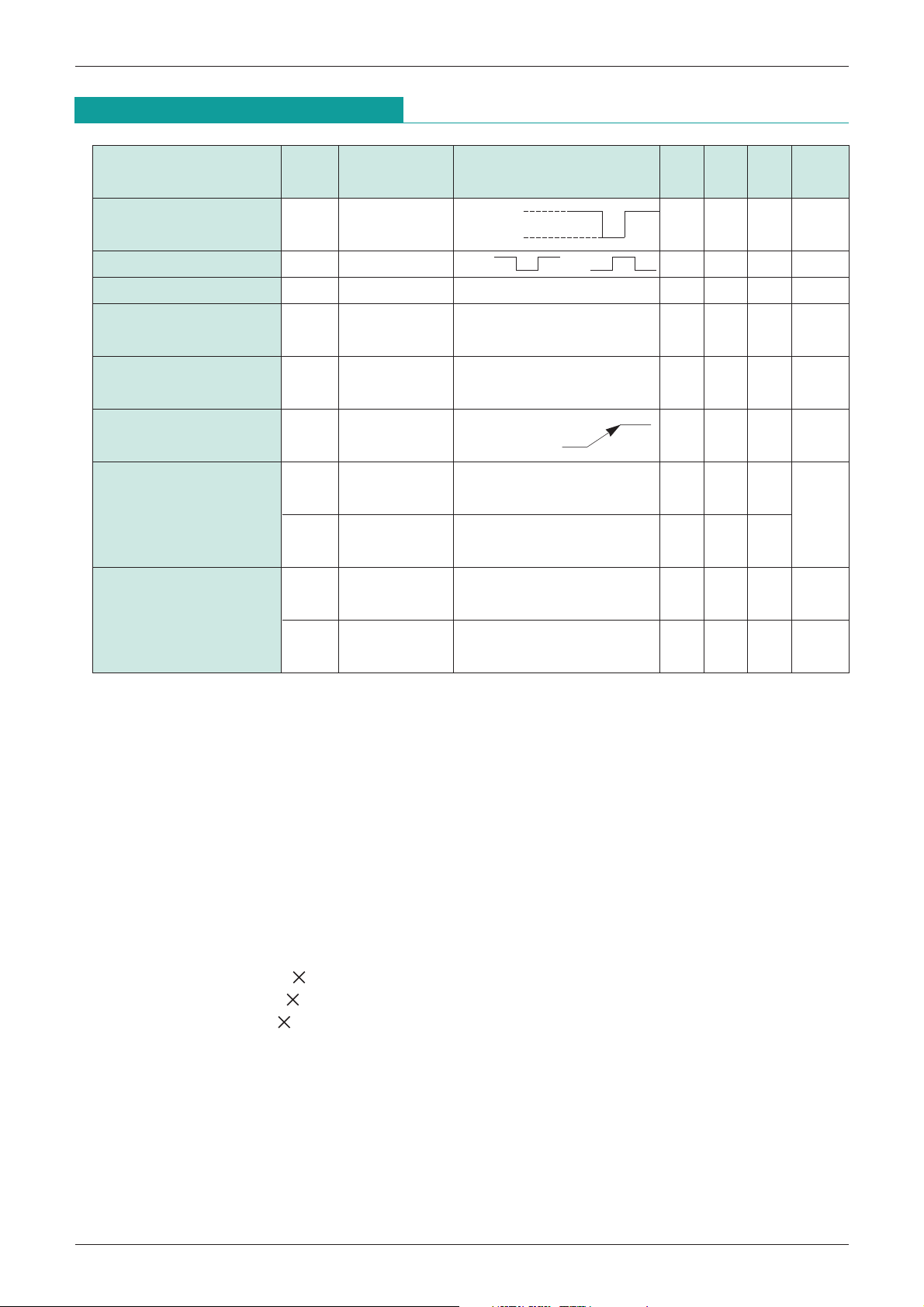
Electrical Characteristics 2 (AC)
(Except where noted otherwise, Ta=25°C, VCC=5V, measurement circuit 2)
Measurement
Item Symbol
Measurement conditions Min. Typ. Max. Units
circuit
5V
CC input pulse width TPI 28µS
V
VCC
4V
CK input pulse width T
CK input cycle T
CKW 23µS
CK 220µS
CK or
Watchdog timer
WD 2CT=0.1µF 5 10 15 mS
monitoring time
1
*
T
Reset time for
WR 2CT=0.1µF 1 2 3 mS
watchdog timer
2
*
T
Reset hold time for
power supply rise
Output delay time from V
3
*
CC
T
PD12
T
CT=0.1µF, VCC
---------------------------------------
RESET
pin
RL1=2.2kΩ, CL1=100pF
210
PR 2 50 100 150 mS
µS
4
*
Output rise time
5
*
PD22
T
R12
t
R22
t
RESET pin
L2=10kΩ, CL2=20pF
R
----------------------------------------
RESET
pin
RL1=2.2kΩ, CL1=100pF
RESET pin
L2=10kΩ, CL2=20pF
R
310
1.0 1.5
µS
1.0 1.5 µS
Notes :
1: Monitoring time is the time from the last pulse (negative edge) of the timer clear clock pulse, until reset
*
pulse output. In other words, reset output is output if a clock pulse is not input during this time.
2: Reset time means reset pulse width. However, this does not apply to power on reset.
*
3: Reset hold time is the time from when VCC exceeds detection voltage (VSH) during power on reset, until
*
---------------------------------------
RESET
4: Output delay time is the time from when power supply voltage drops below detection voltage (VSL), until
*
---------------------------------------
RESET
5: Voltage range when measuring output rise and fall is 10~90%.
*
6: Watchdog timer monitoring time (TWD), watchdog timer reset time (TWR) and reset hold time (TPR) during
*
power supply rise can be changed by varying C
formulae. The recommended range for C
output goes high (reset release).
output goes low (reset status).
PR (mS)
T
T
WD (mS)
T
WR (mS)
.
=. 1000 CT (µF) Example : When CT=0.1µF
.
=. 100 CT (µF) TPR.=. 100mS
.
=. 20 CT (µF) TWD
T capacitance. The times are expressed by the following
T is 0.001~10µF.
.
=. 10mS
.
T
WR
=. 2mS
Page 4

MITSUMI
VCC
CK
C
T
RESET
RESET
V
SH
VSL
TCK
TPR
TWD
TWR
1432
8567
Block Diagram
System Reset (with built-in watchdog timer) MM1035
Note 1: CP = 0.1µF approx.
Note 2: C 1000pF.
~
-
Note 3: The watchdog timer can be stopped by connecting the RCT pin to GND.
(Then it functions as a voltage detection circuit.)
Timing Chart
Pin Assignment
1 TC
2 RESET
3 CK
4 GND
5 V
CC
6 RCT
7 V
S
-----------------------------------------
8 RESET
Page 5

MITSUMI
Pin Description
Pin No. Pin Name Function
System Reset (with built-in watchdog timer) MM1035
1 T
2 RESET Reset output pin (High output)
3 CK Clock input pin (inputs clock from logic system)
4 GND Reset output pin (High output)
5 V
6 RCT
7 VS
8
---------------------------------------------------------------
RESET
Measuring Circuit
Measuring Circuit 1 (DC)
C
TWD, TWR, TPR variable pins. (TWD, TWR and TPR times are determined by
the external capacitor.)
CC 4.2V detection voltage
Watchdog timer stop pin
Operation modes: Operation OPEN, Stop connect to GND
Detection voltage variable pin
Variation modes : Lower pull up resistance, Raise pull down
Reset output pin (Low output)
Measuring Circuit 2 (AC)
Page 6

MITSUMI
System Reset (with built-in watchdog timer) MM1035
Measuring Circuit 1
Item
Consumption current I
Detection voltage
SW Table 6-1-2. SW&Power Supply Table 1
Symbol
SW1 SW2 SW3 SW4 SW5 SW6 SW7 VCC VCK VCT IIRESET VM, IM Notes
CC OFF OFF OFF ON B B ON 5V 5V 0V
SL OFF OFF ON ON B B ON
V
VSH OFF OFF ON ON B B ON
CK input threshold VTH OFF OFF OFF ON B B ON 5V
IH OFF OFF OFF ON B B ON 5V 5V 0V
CK input current
Output voltage (High)
Output voltage (Low)
Output sink current
I
IIL OFF OFF OFF ON B B ON 5V 0V 0V
OH1 ON OFF ON ON B B ON 5V 5V 3V
V
V
OH2 OFF ON ON ON C B ON 5V 5V 3V
OL1 ONONONON B B ON 5V 5V 3V 3mA
V
OL2 ON ON ON ON B B ON 5V 5V 3V 10mA
V
V
OL3 OFF OFF ON ON C B ON 5V 5V 3V
OL4 OFF OFF ON ON C B ON 5V 5V 3V
V
OL1 OFF ON ON ON B C ON 5V 5V 3V
I
IOL2 OFF OFF ON ON B A ON 5V 5V 3V
CT charge current 1 ITC1 OFF OFF OFF ON B B OFF 5V
CT charge current 2 ITC2 OFF OFF ON ON B B OFF 5V
Minimum operating power supply
voltage to ensure reset
Minimum operating power supply
voltage to ensure reset
CCL1 ON OFF ON ON B B ON
V
CCL2 OFF ON ON ON A B ON
V
5V 0V
4V 5V
0V 2V
0V 2V
3V 3V
3V 3V
0V 3V
-
-
0V 0V
0V 0V
1V
1V
1V
----------------------------------------
RESET
--
--
--
--
--
--
-
5µA
--
-
-
--
--
--
--
--
ICC
VO1, CRT1
VO1, CRT1
ICK
ICK
ICK
-
VO1
5µA VO2
-
VO1
-
VO1
0.5mA VO2
1mA VO2
IO1
IO2
ITC
ITC
-
VO1, V
VO2, V
VOO=1V
VOO=1V
CC
CC
Measuring Circuit 2
Item
V
CC input pulse width TPI CB
CK input pulse width T
CK input cycle T
Watchdog timer
monitoring time
Reset time for
watchdog timer
Reset hold time
for power supply rise
Output delay time
CC
from V
Output rise time
Output fall time
Symbol
T
TPD2C A
SW Table 6-2-2. SW&Power Supply Table 2
SW1 SW2 VCCA VCC VCKA VCK CRT Notes
CKW AB 5V
CK AB 5V
WD A A 5V 5V CRT1,2,3
T
WR A A 5V 5V CRT1,2,3
T
PR B A A 5V 5V CRT1,2,3
T
PD1C A
R1 A A 5V 5V CRT1
T
T
R2 A A 5V 5V CRT2
P1 A A 5V 5V CRT1
T
P2 A A 5V 5V CRT2
T
5V
4V
5V
0V
5V
0V
T1
1.4V
-0V
1.4V
0V
1.4V
T2 T3
T2
or
T2 T3
T2
0V
-
-
CRT1,2,3 T1=8µS
-
CRT1,2,3 T2=3µS
-
CRT1,2,3 T3=20µS
0V CRT1,3
0V CRT2,3
Page 7

MITSUMI
Vs pin external resistance
(R1) (kΩ)
4.0
3.5
3.0
100 200 300 400 500 600
V
SH value
V
SL value
Detection voltage
(Vs) (V)
5.0
4.5
100 200 300 400 500 600
Detection voltage
(Vs) (V)
Vs pin external resistance
(R1) (kΩ)
VSH value
V
SL value
System Reset (with built-in watchdog timer) MM1035
Detection Voltage Variation 1
Graph 1. Detection voltage change using MM1035 external resistor
(lowering detection voltage)
Detection voltage can be changed by connecting
resistor R1 externally to MM1035 Vs pin. Determine
R1 according to graph 1 when changing Vs.
Detection Voltage Variation 2
Graph 2. Detection voltage change using MM1035 external resistor
(raising detection voltage)
Detection voltage can be changed by connecting
resistor R2 externally to MM1035 Vs pin. Determine
R2 according to graph 2 when changing Vs.
Page 8

MITSUMI
Clock pulse input time
1.4
1.2
1.0
0.8
0.6
0.4
0.2
1.0 2.0 3.0 4.0 5.0 6.0 7.0 8.0 9.0 10.0
Power supply current Icc
(mA)
Power supply voltage VCC (V)
7.0
6.0
5.0
4.0
3.0
2.0
1.0
1.0 2.0 3.0 4.0 5.0 6.0 7.0 8.0
Ta=20°C.25°C.75°C
PULL UP resistance 10kΩ
Power supply current Icc
(mA)
Power supply voltage VCC (V)
Ta=-25°C
Ta=25
°
C
Ta=75
°
C
7.0
6.0
5.0
4.0
3.0
2.0
1.0
1.0 2.0 3.0 4.0 5.0 6.0 7.0 8.0
PULL UP resistance 2.2kΩ
Output voltage VRESET (V)
Power supply voltage VCC (V)
4.50
4.40
4.30
4.20
4.10
4.00
3.00
-40-
20 0 20 40 60 80 100
Ambient temperature Ta (°C)
VSH
VSL
Detection voltage (V)
Ta=75°C
Ta=25
°
C
Ta=
-
25°C
500
400
300
200
100
0.2 0.4 0.6 0.8 1.0 1.2 1.4 1.6 1.8
Output saturation voltage
V
OL (mV)
Output sink current IOL (mA)
500
400
300
200
100
2 4 6 8 10 12 14 16 18
Ta=75°C
Ta=25
°
C
Ta=
-
25°C
Output saturation voltage
V
OL (mV)
Output sink current IOL (mA)
Characteristics
System Reset (with built-in watchdog timer) MM1035
Power supply current-Power supply voltage
Output voltage-Power supply voltage (RESET
------------------------------------------------------------------
pin)
Output voltage-Power supply voltage (RESET pin)
Detection voltage (V
SL
, VSH) temperature (RESET, RESET
---------------------------------------------------------------------------
pins)
Output saturation voltage-Output sink current (RESET
----------------------------------------------------------------
pin)
Output saturation voltage-Output sink current (RESET
------------------------------------------------------------------------------
pin)
Page 9

MITSUMI
5.0
4.8
4.6
4.4
4.2
4.0
3.8
-2-4-6-8-10-12-14-16-
18
High level output voltage
V
OM (V)
High level output current IOM (µA)
5.0
4.8
4.6
4.4
4.2
4.0
3.8
-2-4-6-8-10-12-14-16-
18
High level output voltage
V
OM (V)
High level output current IOM (µA)
160
140
120
100
80
60
40
-40-
20 0 20 40 60 80 100
VCC=5V (Cr=0.1µF)
Reset hold time temperature during
power supply rise T
PR (mS)
Ambient temperature Ta (°C)
16
14
12
10
8
6
4
-40-
20 0 20 40 60 80 100
VCC=5V (Cr=0.1µF)
Watchdog timer monitoring time
temperature T
WD (mS)
Ambient temperature Ta (°C)
3.5
3.0
2.5
2.0
1.5
1.0
0.5
-40-
20 0 20 40 60 80 100
VCC=5V (Cr=0.1µF)
Reset time TWR (mS)
Ambient temperature Ta (°C)
10
5
10
4
10
3
10
2
10
1
10
-
310-
210-
1100
10
0
10
1
Hold time TWD (mS)
CT capacitance (µF)
System Reset (with built-in watchdog timer) MM1035
High level output voltage-High level
output current (RESET pin)
Reset hold time temperature during power
supply rise
High level output voltage - High level output current
------------------------------------------------
(RESET
pin)
Watchdog timer monitoring time temperature
Reset time temperature (for watchdog timer)
CTvalue for reset hold time during power supply rise
Page 10

MITSUMI
10
3
10
2
10
1
10
0
10
-
1
10
-
2
10
-
310-
210-1100101
Reset time TWR (mS)
CT capacitance (µF)
10
4
10
3
10
2
10
1
10
0
10
-1
10
-
310-
210-
1100101
Timer monitoring time TWD (mS)
CT capacitance (µF)
System Reset (with built-in watchdog timer) MM1035
CTvalue for reset time (for watchdog timer)
CTvalue for watchdog timer monitoring time
 Loading...