

Page 1

MITSUMI
S Video Amplifier MM1029
S Video Amplifier
Monolithic IC MM1029
Outline
This is a video amp IC that supports S and also has a superimpose function.
Amp gain is as follows : 6dB for Y signal amplification, 10dB for C signal amplification and 6dB for composite
signal amplification. A 75Ω driver is built in.
Features
1. Supports S-VHS
2. Built-in superimpose function
3. Built-in Y-C mix circuit
4. Vertical/horizontal sync signal output pin
5. Amp gain : 6dB for Y signal, 10dB for C signal and 6dB for composite signal
6. Built-in clamp circuit (for Y signal only)
7. Built-in monitor cut function
8. 75Ω driver built in
9. Frequency response Y : 7MHz
C : 5MHz
10.Power supply voltage 4.7V~5.3V
Package
SOP-16A (MM1029AF)
Applications
1. TV
2. VCR
3. VCR with camera
4. Other video equipment
Page 2
MITSUMI
S Video Amplifier MM1029
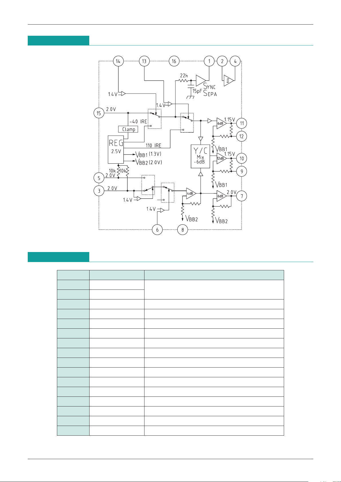
Block Diagram
Pin Description
Pin no. Pin name Function
1 R
Integrates sync signal and inputs to Schmidt circuit
2 C
3 PB
IN Chroma signal input pin for other than playback
4 V
SYNC OUT Vertical sync signal output pin
5 PB
IN Chroma signal input pin for playback
6 Chroma mute input Chroma mute signal input pin
7 C
HROMA OUT Chroma signal output pin
8 GND
9 SUG Anti-sag pin
10 V
IDEO OUT Composite video signal output pin
11 Y
OUT Y (luminance) signal output pin
12 SUG Anti-sag pin
13 Character input Character input pin for superimpose
14 Monitor cut V insert Monitor cut V insert pin
15 Y
OR VIDEO IN Luminance or video signal input pin
16 V
CC
Page 3

MITSUMI
S Video Amplifier MM1029
Absolute Maximum Ratings
(Ta=25°C)
Electrical Characteristics
(Except where noted otherwise, Ta=25°C, VCC=5.0V, pulse level 0V, SW1 : A, SW2 : B)
Item Symbol Ratings Units
Storage temperature T
STG
-
40~+125 °C
Operating temperature T
OPR
-
20~+75 °C
Power supply voltage V
CC max. 7 V
Allowable loss Pd 350 mW
Item
Symbol
Measurement
Measurement conditions Min. Typ. Max. Units
circuit
Operating power supply voltage
VCC VCC 4.7 5.0 5.3 V
Consumption current Id
-
SG-1, SG-2, SG-3 : No signal
25.0 33.0 mA
Measure with DC ammeter.
Y amp output
Voltage gain G
V1 TP11 SG
-
1 Sweep signal 1VP
-
P, 0.1MHz 5.5 6.0 6.5 dB
Differential gain DG1 TP10
SG
-
1 Staircase wave 1VP
-
P
1.0 3.0 %
APL=10, 50, 90%
Differential phase DP1 TP10
SG
-
1 Staircase wave 1VP
-
P
1.0 3.0 deg
APL=10, 50, 90%
Frequency characteristic fc1 TP11
SG
-
1 Sweep signal 1VP
-
P
-
1.0 0 1.0 dB
5MHz/0.1MHz
*
1
Video amp output
Voltage gain G
V2 TP8 SG
-
1 Sweep signal 1VP
-
P, 0.1MHz 5.5 6.0 6.5 dB
Differential gain DG2 TP9
SG
-
1 Staircase wave 1VP
-
P
1.0 3.0 %
APL=10, 50, 90%
Differential phase DP2 TP9
SG
-
1 Staircase wave 1VP
-
P
1.0 3.0 deg
APL=10, 50, 90%
Frequency characteristic fc2 TP8
SG
-
1 Sweep signal 1VP
-
P
-
1.0 0 1.0 dB
5MHz/0.1MHz
*
1
Chroma amp output
Voltage gain G
V3 TP7
SG-2 Sine wave 0.2V
P-P
, 0.1MHz
9.0 10.0 11.0 dB
Frequency characteristic fc3 TP7
SG
-
2 Sine wave 0.2VP
-
P
-
1.0 0 1.0 dB
5MHz/0.1MHz
*
1
Crosstalk
Crosstalk 1 Y
IN COUT CT1 TP7
SG-1 Sine wave 1.0V
P-P
, 4MHz *2
-
36-30 dB
Crosstalk 2 P
B YOUT
CT2 TP11
SG-2 Sine wave 0.2V
P-P
, 4MHz *3
-
42-36 dB
Crosstalk 3 P
B YOUT CT3 TP11
SG-3 Sine wave 0.2V
P-P
, 4MHz *3
-
42-36 dB
Crosstalk 4 P
B COUT CT4 TP7
SG-1 Sine wave 0.2V
P-P
, 4MHz *4
-
50-40 dB
Superimpose
V insertion level Y V
MCY TP10
SG-1 Staircase wave (no chroma signal) 1V
P-P
-
45-40-35 IRE
TP13 Pulse level 5V
V insertion level V V
MCV TP9
SG-1 Staircase wave (no chroma signal) 1V
P-P
-
45-40-35 IRE
TP13 Pulse level 5V
Character level Y V
CHY TP10
SG-1 Staircase wave (no chroma signal) 1V
P-P
105 110 115 IRE
TP12 Pulse level 5V
Character level V V
CHV TP9
SG-1 Staircase wave (no chroma signal) 1V
P-P
105 110 115 IRE
TP12 Pulse level 5V
Input threshold voltage
V insertion input V
TH1 TP13
SG-1 Staircase wave (no chroma signal) 1V
P-P
0.7 1.4 2.1 V
TP13 Pulse level L H
*
5
Character input V
TH2 TP12
SG-1 Staircase wave (no chroma signal) 1V
P-P
0.7 1.4 2.1 V
TP12 Pulse level L H
*
5
Chroma mute input V
TH3 TP5
SG-2 Sine wave 0.1V
P-P
, 4MHz
0.7 1.4 2.1 V
TP5 Pulse level L H
*
6
Sync separation
Sync separation level V
SEPA TP14
SG-1 Staircase wave (no chroma signal) 1V
P-P
55 110 165 mV
SG-1 SYNC level, max min *7
Schmitt trigger VTH4H
TP1
TP1 DC voltage 0V H
*
8 1.9 2.1 2.3 V
threshold voltage V
TH4L TP1 DC voltage 5V L
*
8 1.1 1.3 1.5 V
Vertical sync output voltage
V
VH
TP3
TP1 DC voltage 5V L
*
9 4.8 5.0 V
V
VL TP1 DC voltage 0V H
*
9 0.2 0.4 V
Page 4

MITSUMI
S Video Amplifier MM1029
Notes :
*
1 1. Voltage gain GV1, GV2, GV3
Given SG-1 input as V1 and TP11 output signal as V2, G
V1 is obtained as follows.
The same applies for G
V2 and GV3.
V2
G
V1=20LOG [dB]
V1
2. Frequency response f
C1, fC2, fC3
For the same conditions as the G
V1 measurement, given TP11 output for 0.1MHz as V3, and
for 5MHz as V1, F
C1 is obtained as follows. The same applies for fC2 and fC3.
V4
F
C1=20LOG [dB]
V3
*
2 Crosstalk Yin COUT CT1
Given TP14 input signal as V5 and TP7 output signal as V6, C
T1 is obtained as follows.
V6
C
T1=20LOG [dB]
V5
*
3 Crosstalk PB, PB YOUT CT2, CT3
Give TP2 and TP4 input signals as V7, and TP11 output signal as V8, C
T2 and CT3 are obtained
as follows.
V8
*
1
C
T2=20LOG
-
4 [dB]
V7
*
1 When C is input to compare between YIN COUT and CIN YOUT, subtract the 4dB amp
portion from crosstalk.
*
4 Crosstalk PB COUT CT4
Given TP4 input signal as V9 and TP7 output signal as V10, CT4 is obtained as follows.
V10
C
T4=20LOG [dB]
V9
*
5 Input threshold voltage V insert input, character input VTH1, VTH2
For the same conditions as V
MCY and VCHY measurement, raise TP13 and TP12 pulse levels
gradually. TP13 and TP12 pulse levels when V insert signal and character signal appear on TP11
are, respectively, V
TH1 and VTH2.
*
6 Input threshold voltage Chroma mute input VTH3
Gradually raise TP5 pulse level. TP5 pulse level when a sine wave is no longer output on TP7 is
V
TH3.
*
7 Sync separation level VSEPA
Gradually reduce SG-1 SYNC level from maximum to minimum. Measure the SYNC signal level at
TP14 when a sync separation signal is no longer output on TP15 to obtain V
SEPA.
*
8 Schmidt trigger threshold level VTH4H, VTH4L
Impress external DC voltage on TP1 and gradually raise from 0V. TP1 level when TP3 level goes
from high to low is V
TH4H. Gradually lower from 5V. TP1 level when TP3 level goes from low to
high is V
TH4L.
*
9 Vertical sync output voltage VVH, VVL
TP3 low level for TTH4H measurement is VVL, and TP3 high level for VTH4L is VVH.
Page 5

MITSUMI
S Video Amplifier MM1029
Measuring Circuit
Application Circuits
 Loading...