

Page 1
MITSUMI
System Reset (with battery back-up) MM1025, 1174
System Reset (with battery back-up)
Monolithic IC MM1025, 1174
Outline
These ICs were developed for D-RAM and dummy S-RAM battery back-up. D-RAM and dummy S-RAM
power supplies differ from that of S-RAMs because 5V or 3.3V of power supply is required even during
battery back-up. Therefore, these ICs provide voltage from a stable power supply during both normal
operation and back-up. Also, the internal stable power supply switches automatically to battery back-up if the
main power supply voltage goes down for any reason.
Features
1. Battery back-up
MM1025
Current consumption 600µA typ.
Input/output voltage difference I
Output current 40mA max.
MM1174
Current consumption 300µA typ.
Input/output voltage difference I
Output current 40mA max.
2. Normal operation
MM1025
Input/output voltage difference I
Output current V
External transistor drive current V
Current consumption 900µA max.
MM1174 (for external transistor)
Input/output voltage difference I
Output current Depends on external transistor
External transistor drive current (no built-in TR) V
Current consumption 500µA max.
L=40mA 0.25V typ.
L=40mA 0.13V typ.
L=80mA (built-in transistor) 0.29V typ.
CC=6V 80mA typ.
CC= 6V 15mA typ.
L=200mA 0.13V typ.
CC=3.6V 10mA typ.
3. Switching voltage from V
MM1025 4.9V typ.
MM1174 3.25V typ.
4. V
CC-Battery forced switching and detection voltage adjustment possible
CC to Battery VCC=High Low
Package
SOP-8A
Applications
1. Memory cards (D-RAM cards, other)
2. PCs, word processors and other equipment with D-RAMs
3. Fax machines, photocopiers and other office equipment with D-RAMs
Page 2
MITSUMI
1432
8567
SOP-8P (A)
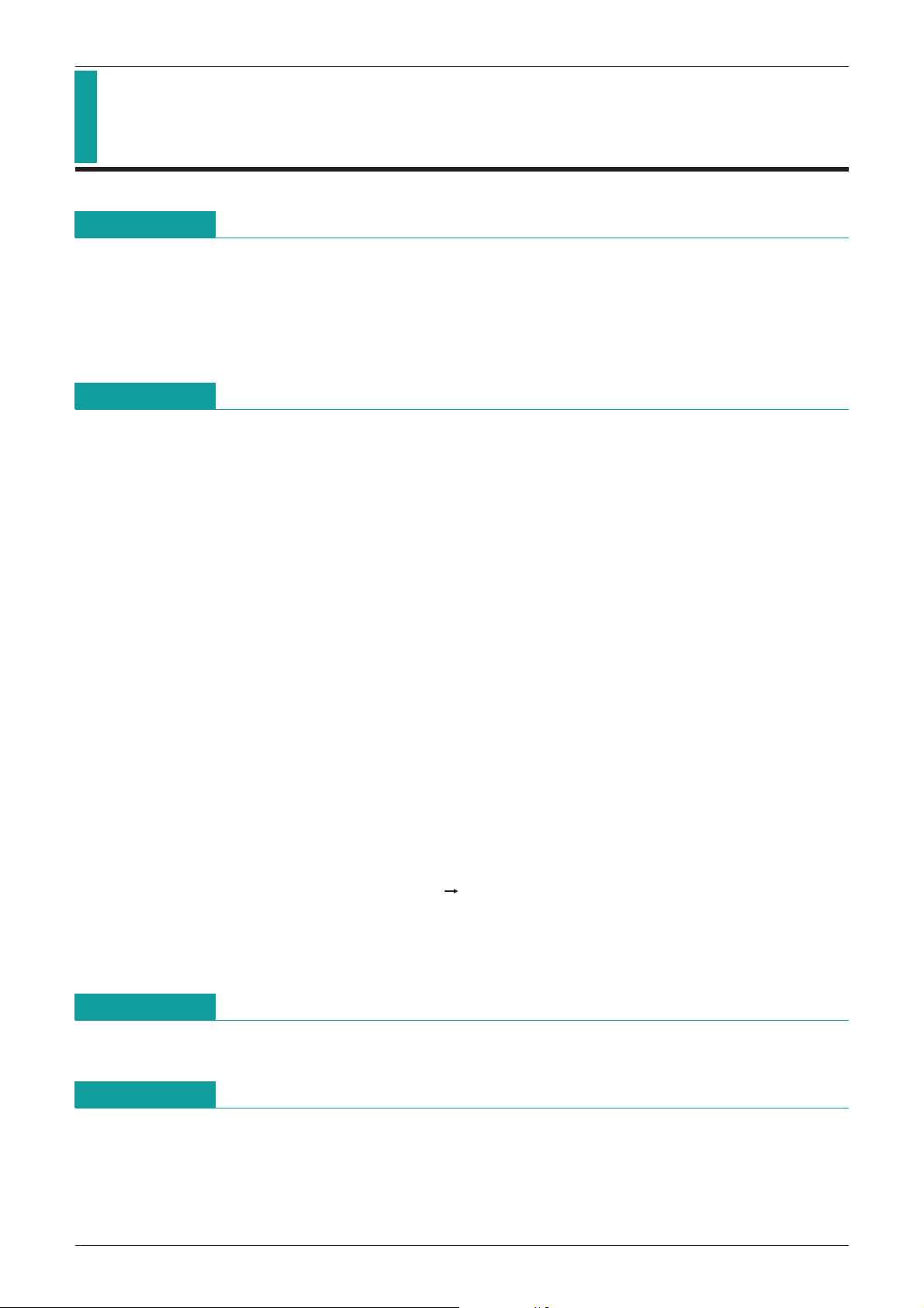
Pin Assignment
System Reset (with battery back-up) MM1025, 1174
1
2 GND
3 GND
4 CS
Pin Description
Pin No. Pin name Function
1 Forced switching and detection voltage adjustment
2 GND
3 GND
4 CS
5 V
6 VOUT
7 VCC
8 TRB External transistor drive
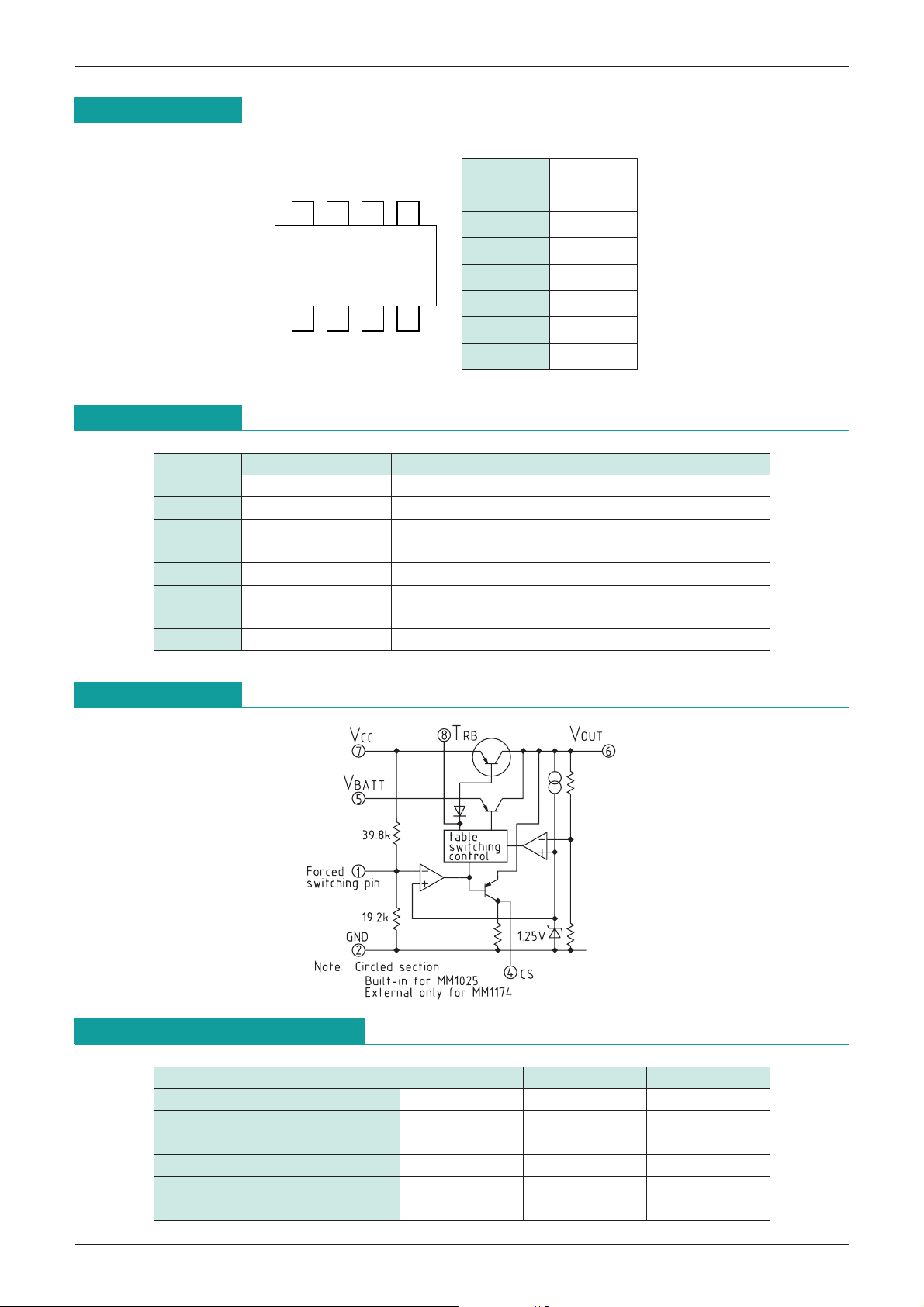
Block Diagram
BATT
5 V
BATT
6 VOUT
7 VCC
8 TRB
Absolute Maximum Ratings
Item Symbol Rating Units
Operating temperature T
Storage temperature T
Maximum output current 1 I
Maximum output current 2 I
Power supply voltage V
Power consumption Pd 300 mW
(Ta=25°C)
OPR
STG 40~+125
L max. 80 mA
L max. 40 mA
CC
-
20~+70
-
0.3~+18 V
°
C
°
C
Page 3

MITSUMI
VCC
VBATT
VOUT
CS
VCC
VCC
VOUT
VCSL
VHYS
VTHI
VOUT- VCSH
System Reset (with battery back-up) MM1025, 1174
Electrical Characteristics
(Ta=25°C)
Item Symbol Measurement conditions Min. Typ. Max. Units
Consumption MM1025
current 1 MM1174 V
I/O voltage MM1025
V
difference 1
1 MM1174 VCC=3.0V, VBATT=0V, IL=200mA 0.13 020
*
Consumption MM1025
I
current 2 MM1174 V
I/O voltage MM1025
V
difference 2 MM1174 V
MM1025
Output voltage
VOUT
MM1174 V
Load fluctuation
MM1025
REG
rate MM1174 VCC=0V, VBATT=3.6V, IL=0~20mA 0.05
Input fluctuation
MM1025
REG
rate MM1174 V
Output voltage MM1025
TC
emperature coefficient
MM1174 VCC or VBATT=3.6V, IL=3mA 0.01
CC
I
SAT1
BATT
SAT2
VO
VCC=6V, VBATT=0V, IL=0mA 0.6 0.9 1.20
mA
CC=3.6V, VBATT=0V, IL=0mA 0.25 0.50 1.00
CC=5V, VBATT=0V, IL=80mA 0.15 0.29 0.40
V
V
VCC=0V, VBATT=6V, IL=0mA 400 600 780
µA
CC=0V, VBATT=3.6V, IL=0mA 150 300 600
V
CC=0V, VBATT=5V, IL=40mA 0.15 0.25 0.40
V
CC=0V, VBATT=3.0V, IL=20mA 0.13 0.20
VCC=6V or VBATT=6V, IL=5mA 4.8 5.0 5.2
V
CC=3.6V or VBATT=3.6V, IL=3mA 3.14 3.27 3.40
-
L
V
-
IN
CC or VBATT=5.5~10V, IL=5mA 0.05
CC or VBATT=3.6V~10V, IL=3mA 0.05
VCC or VBATT=6V, IL=5mA 0.01
VCC: IL=0-80mA, V
BATT
: IL=0-40mA
0.05
%/mA
%/V
°
C
%/
Switching voltage
MM1025
(H L) MM1174 V
Hysteresis MM1025
voltage MM1174 V
Maximum base MM1025
I
driving current MM1174 V
CS output MM1025
voltage H MM1174 V
CS output MM1025
voltage L MM1174 V
Timing Chart
TH1
V
HYS
V
B max.
CSH
V
CSL
V
V
CC=6V 4V, VBATT=6V, IL=40mA 4.8 4.9 5.1
CC=4V 3V, VBATT=3.6V, IL=3mA 3.1 3.25 3.4
VCC=4V 6V, VBATT=6V, IL=40mA 100 200 400
CC=3V 4V, VBATT=3.6V, IL=3mA 15 30 60
V
CC=6V, VCC Ampere meter 8PIN 9.0 15.0 20.0
CC=3.6V, VCC Ampere meter 8PIN 5.0 10.0 20.0
VCC=6V, VBATT=6V, VOUT-VCS 0.10 0.50
CC=3.6V, VBATT=3.6V, VOUT
-
VCS 0.10 0.50
VCC=4V, VBATT=6V 0.50
CC=3.0V, VBATT=3.6V 0.50
V
mV
mA
V
V
Page 4

MITSUMI
IBATT
(mA)
1.000
1000
0000
0000
/div
10.00
VBATT 1.000/div (V)
.0000
5.000
.5000
/div
(V)
V
OUT
(RL=120Ω)
VOUT
ICC
IBATT
(mA)
100.0
10.00
.0000
.0000
/div
V
BATT 1.000/div (V)
.0000
5.000
.5000
/div
(R
L=120Ω)
(V)
V
OUT
10.00
VOUT
ICC
10.00
I
CC
(mA)
2.000
2000
.0000
.0000
/div
VCC 1.000/div (V)
.0000
5.000
.5000
/div
(RL=∞)
(V)
V
OUT
VOUT
ICC
ICC
(mA)
100.0
10.00
.0000
/div
10.00
.0000
VBATT 1.000/div (V)
(R
L=∞)
.0000
5.000
.5000
/div
(V)
V
OUT
VOUT
ICC
6.000
V
OUT
(V)
5.000
.5000
.0000
4.0000
/div
VCC .2000/div (V)
.0000
100.0
10.00
/div
(mA)
I
CC
(Ta = ambient temperature)
System Reset (with battery back-up) MM1025, 1174
Characteristics
(MM1025 series)
Output voltage and current consumption
CC voltage supply
for V
Output voltage and current consumption
CC voltage supply
for V
Output voltage and current consumption for
battery voltage supply
Output voltage and current consumption for
battery voltage supply
Power supply switching voltage
Page 5

MITSUMI
5.0
4.8
4.6
0 500 1000
V
CC=6.0V
V
BATT=0V
IL (mA)
Output voltage (V)
External Tr 2SA1020Y
200406070
4.6
4.8
5.0
IL (mA)
VCC=0V
V
BATT=6.0V
Output voltage (V)
0
4.6
4.8
5.0
50 100
IL (mA)
VCC=6.0V
V
BATT=0V
Output voltage (V)
(No external power transistor)
Current consumption 2
-
25 0 25 50 75
500
450
400
350
300
Current consumption (µA)
Temperature (°C)
Current consumption 1
50 100 150 200 250
IOUT (mA)
3.0
2.8
2.6
2.4
2.2
2.0
Output voltage (V)
2.87V
2.85V
2.80V
I
L=-20mA
3.0
2.8
2.6
-
25 0 25 50 75
Output voltage (V)
Temperature (°C)
VOUT=3mA
3.3
3.2
3.1
-
25 0 25 50 75
Output voltage (V)
Temperature (°C)
VCC output current (external power transistor)
VBATT output current
VCC output current (no external power transistor)
System Reset (with battery back-up) MM1025, 1174
Characteristics
Current consumption 1-2 temperatures
Input/output voltage difference 2 temperature
(MM1174 series)
Input/output voltage difference 1
temperature (external transistor 2SA1020)
Output voltage-Temperature
Page 6

MITSUMI
20
15
10
5
-
25 0 25 50 75
Base current (mA)
Temperature (°C)
CS output voltage L
CS output voltage H
3.3
3.2
3.1
-
25 0 25 50 75
100
(mV)
CS output voltage H (V)
Temperature (°C)
CS output voltage L
IBUFF
IBUFF (mA)
20.00
2.000/div
.0000
.0000 10.00
1.000/div
V
CC (V)
IBATT
IBATT
ICC
ICC
IBUTT (mA)
5.000
.5000/div
.0000
2.750
I
CC
(mA)
5.000
.5000/div
.0000
2.950
.0200/div
V
CC (V)
VCS
(V)
5.0000
.500/div
.0000
0.0000
10.00
1.000/div
V
CC (V)
VOUT (V)
5.0000
.5000/div
.0000
V
OUT
VOUT
VCS
System Reset (with battery back-up) MM1025, 1174
Maximum base drive current-Temperature
Base drive current
CS output voltage H-L temperature
VCC-ICC, IBATT
VCC-VOUT, VCS
 Loading...