

Datasheet ML4825IS, ML4825IP, ML4825IQ, ML4825CQ, ML4825CP Datasheet (Micro Linear Corporation)
...Page 1

May 1997
ML4825*
High Frequency Power Supply Controller
GENERAL DESCRIPTION
The ML4825 High Frequency PWM Controller is an IC
controller optimized for use in Switch Mode Power
Supply designs running at frequencies to 1MHz.
Propagation delays are minimal through the comparators
and logic for reliable high frequency operation while slew
rate and bandwidth are maximized on the error amplifier.
This controller is designed to work in either voltage or
current mode and provides for input voltage feed forward.
FEATURES
■ Practical operation at switching frequencies to 1.0MHz
■ High current (2A peak) dual totem pole outputs
■ Wide bandwidth error amplifier
■ Fully latched logic with double pulse suppression
■ Pulse-by-pulse current limiting
■ Soft start and maximum duty cycle control
■ Under voltage lockout with hysteresis
A 1V threshold current limit comparator provides cycleby-cycle current limit while exceeding a 1.4V threshold
initiates a soft-start cycle. The soft start pin doubles as a
maximum duty cycle clamp. An under-voltage lockout
circuit with 800mV of hysteresis assures low startup
current and drives the outputs low.
This controller is similar in architecture and performance
to the UC1825 controller, however the ML4825 includes
many features not found on the 1825. These features are
set in
Italics
.
■ Precision trimmed 5.1V bandgap reference
■ Pin compatible improved replacement for UC1825
■
Fast shut down path from current limit to outputs
■
Outputs preset to known condition after under voltage
lockout
■
Soft start latch ensures full soft start cycle
■
Outputs pull low for undervotage lockout
BLOCK DIAGRAM (Pin configuration shown for 16-pin version) *Some Packages Are Obsolete or End Of Life
R
T
5
C
T
6
OSC
CLOCK OUT
4
RAMP
7
E/A OUT
3
NI
2
INV
1
SS
8
I
LIM
9
/SD
1V
1.4V
1.25V
+
ERROR
AMP
+
–
–
+
+
–
9µA
COMP
+
–
C
V+
R
S
Q
TF.F.
Q
P
–
+
1V
Q
UNDER
VOLTAGE
LOCKOUT
R
S
Q
PWR V
C
13
OUT A
11
POWER GND
POWER V
ENABLE
V
REF
9V
–
+
V
REF
GEN
INTERNAL
BIAS
C
PWR GND
+
4V
–
1.5V V
SIGNAL GND
OUT B
REF
V
CC
14
12
16
15
10
1
Page 2

ML4825
PIN CONFIGURATION
ML4825
16-Pin PDIP
ML4825
20-Pin PLCC
16-Pin SOIC
INV
E/A OUT
CLOCK
RAMP
1
NI
2
3
4
R
5
T
C
6
T
7
SS
8
TOP VIEW
16
15
14
13
12
11
10
9
5.1V REF
V
CC
OUT B
V
C
PWR GND
OUT A
GND
I
/SD
LIM
E/A OUT
CLOCK
NC
R
C
NI
INVNC5.1V REF
3212019
4
5
6
7
T
8
T
910111213
SS
RAMP
TOP VIEW
PIN DESCRIPTION (Pin number in parentheses is for PLCC version)
PIN NAME FUNCTION PIN NAME FUNCTION
1 (2) INV Inverting input to error amp.
2 (3) NI Non-inverting input to error amp.
3 (4) E/A OUT Output of error amplifier and input
to main comparator
4 (5) CLOCK Oscillator output
9 (12) I
/SD Current limit sense pin. Normally
LIM
connected to current sense resistor.
10 (13) GND Analog signal ground
11 (14) OUT A High current totem pole output. This
output is the first one energized after
power on reset
NC
/SD
LIM
I
CC
V
18
17
16
15
14
GND
OUT B
V
C
NC
PWR GND
OUT A
5 (7) R
T
Timing resistor for oscillator—
sets charging current for oscillator
timing capacitor (pin 6)
6 (8) C
T
Timing capacitor for oscillator
7 (9) RAMP Non-inverting input to main
comparator. Connected to CT for
voltage mode operation or to current
sense resistor for current mode
8 (10) SS Normally connected to soft start
capacitor
12 (15) PWR GND Return for the high current totem
pole outputs
13 (17) V
C
Positive supply for the high current
totem pole output
14 (18) OUT B High current totem pole output
15 (19) V
CC
Positive supply for the IC
16 (20) 5.1V REF Buffered output for the 5.1V voltage
reference
2
Page 3

ABSOLUTE MAXIMUM RATINGS
ML4825
Absolute maximum ratings are those values beyond which
the device could be permanently damaged. Absolute
maximum ratings are stress ratings only and functional
device operation is not implied.
Supply Voltage (V
) ........................................... 30V
C, VCC
Output Current, Source or Sink (OUT A, OUT B)
Junction Temperature
ML4825IX, ML4825CX ....................................... 150°C
Storage Temperature Range ..................... –65°C to 150°C
Lead Temperature (soldering 10 sec.) ..................... 260°C
Thermal Resistance (θ
)
JA
Plastic DIP or SOIC ......................................... 65°C/W
Plastic Chip Carrier (PCC) ................................ 60°C/W
DC ....................................................................... 0.5A
Pulse (0.5µs) ......................................................... 2.0A
Analog Inputs
OPERATING CONDITIONS
(INV, NI, RAMP)................................ GND –0.3V to 7V
(SS, I
CLOCK Output Current ...........................................–5mA
E/A OUT Output Current .......................................... 5mA
Soft Start Sink Current ............................................ 20mA
) ........................................... GND –0.3V to 6V
LIM
Temperature Range
ML4825CX ................................................ 0°C to 70°C
ML4825IX .............................................. –40°C to 85°C
RT Charging Current ................................................–5mA
ELECTRICAL CHARACTERISTICS
Unless otherwise specified, R
PARAMETER CONDITIONS MIN TYP MAX UNITS
OSCILLATOR
Initial Accuracy T
Voltage Stability 10V < VCC < 30V, T
Temperature Stability 5%
Total Variation Line, temperature 340 460 kHz
Clock Out High 3.9 4.5 V
Clock Out Low 2.3 2.9 V
Ramp Peak 2.6 2.8 3.0 V
Ramp Valley 0.7 1.0 1.25 V
Ramp Valley to Peak 1.6 1.8 2.0 V
REFERENCE
Output Voltage T
Line Regulation 10V < VCC < 30V –20 2 20 mV
Load Regulation 1mA < IO < 10mA –20 5 20 mV
Temperature Stability –55°C < TJ < 150°C 0.2 0.4 %
Total Variation Line, load, temperature C suffix 4.95 5.25 V
Output Noise Voltage 10Hz to 10kHz 50 µV
Long Term Stability T
Short Circuit Current V
ERROR AMPLIFIER
Input Offset Voltage C suffix –15 15 mV
Input Bias Current 0.6 3 µA
Input Offset Current 0.1 1 µA
Open Loop Gain 1 < VO < 4V 60 96 dB
= 3.65kΩ, C
T
= 1000pF, TA = Operating Temperature Range, VCC = 15V (Note 1).
T
= 25°C 360 400 440 kHz
J
= 25°C –2 0.2 2 %
A
= 25°C, I
J
= 125°C, 1000 hours 5 25 mV
J
= 0V –15 –50 –100 mA
REF
I suffix –15 15 mV
= 1mA C suffix 5.00 5.10 5.20 V
O
I suffix 5.00 5.10 5.20 V
I suffix 4.95 5.25 V
3
Page 4

ML4825
ELECTRICAL CHARACTERISTICS (Continued)
PARAMETER CONDITIONS MIN TYP MAX UNITS
ERROR AMPLIFIER (Continued)
CMRR 1.5V < VCM < 5.5V C suffix 75 95 dB
I suffix 75 95 dB
PSRR 10V < VCC < 30V C suffix 80 110 dB
I suffix 80 110 dB
Output Sink Current V
Output Source Current V
Output High Voltage I
Output Low Voltage I
EA OUT A
EA OUT A
EA OUT A
EA OUT A
Unity Gain Bandwidth 3 5.5 MHz
Slew Rate 612 V/µs
PWM COMPARATOR
Ramp Bias Current V
RAMP
Duty Cycle Range C suffix 85 100 %
E/A OUT Zero DC Threshold V
RAMP
Delay to Output 50 80 nS
SOFT START
Charge Current SS = 0.5V –3 –9 –20 µA
Discharge Current SS = 1V 1 mA
CURRENT LIMIT/SHUTDOWN
I
Bias Current 0V < V
LIM
Current Limit Threshold 0.9 1 1.1 V
Shutdown Threshold T
A
T
A
Delay to Output 40 70 ns
OUTPUT
Output Low Level I
Output High Level I
Collector Leakage V
OUT
I
OUT
OUT
I
OUT
C
Rise/Fall Time CL = 1000pF 30 60 ns
UNDERVOLTAGE LOCKOUT
Start Threshold 8.8 9.2 9.6 V
UVLO Hysteresis 0.3 0.8 1.2 V
SUPPLY
Start Up Current VCC = 8V C suffix 0.1 1.1 2.5 mA
I
CC
V
INV, VRAMP, VI(LIM)/SD
VNI = 1V, T
Note 1: Limits are guaranteed by 100% testing, sampling, or correlation with worst-case test conditions.
= 1.0V 1 2.5 mA
= 4.0V –0.5 –1.3 mA
= –0.5mA 4.0 4.7 5.0 V
= 1mA 0 0.5 1.0 V
= 0V, T
> 0°C C suffix –1 –5 µA
A
I suffix –5 µA
I suffix 80 100 %
= 0V 1.1 1.25 1.7 V
< 0.5V C suffix –10 10 µA
I(LIM)
I suffix –10 10 µA
> 0°C 1.25 1.4 1.55 V
< 0°C 1.25 1.4 1.60 V
= 20mA 0.25 0.4 V
= 200mA 1.2 2.2 V
= –20mA 13.0 13.5 V
= –200mA 12.0 13.0 V
= 30V 100 500 µA
I suffix 0.1 3.5 mA
= 0V, 10 26 33 mA
= 25°C
A
4
Page 5
ML4825
FUNCTIONAL DESCRIPTION
OSCILLATOR
The ML4825 oscillator charges the external capacitor (CT)
with a current (I
voltage reaches the upper threshold (Ramp Peak), the
comparator changes state and the capacitor discharges to
the lower threshold (Ramp Valley) through Q1. While the
capacitor is discharging, Q2 provides a high pulse.
The oscillator period can be described by the following
relationship:
t
= t
OSC
where:
t
=
RAMP
and:
t
DEADTIME
) equal to 3/R
SET
+ t
RAMP
C Ramp Valley to Peak
DEADTIME
()
I
SET
C Ramp Valley to Peak
()
=
I
. When the capacitor
SET
Q
1
100k
100nF
47nF
22nF
0nF
10k
(Ω)
T
R
4.7nF
2.2nF
1nF
470pF
1k
100 1k 10k
FREQUENCY (Hz)
100k
1M
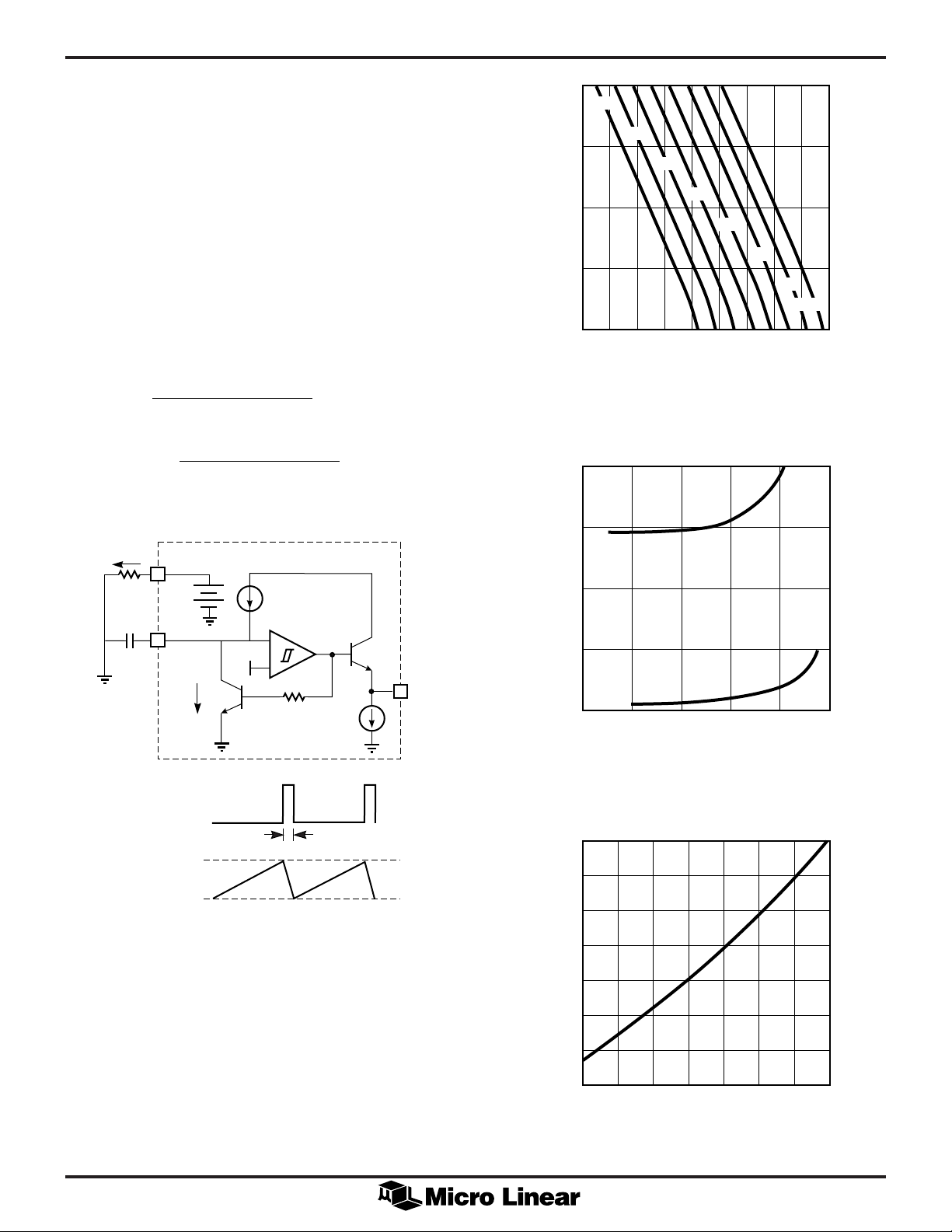
Figure 2. Oscillator Timing Resistance vs Frequency
160
140
1.0nF
I
SET
5
R
T
3V
6
I
Q1
C
T
CLOCK
RAMP PEAK
RAMP VALLEY
Q1
t
D
C
T
5.1V
I
SET
+
–
Figure 1. Oscillator Block Diagram
120
(ns)
D
T
100
4
80
10k 100k 1M
470pF
FREQUENCY (Hz)
Figure 3. Oscillator Deadtime vs Frequency
4.70
2.20
1.00
(µs)
D
0.47
T
0.22
0.10
0.047
1.0 4.7 4710.0
0.47 2.2 100
CT (nF)
Figure 4. Oscillator Deadtime vs C
22
(3kΩ ≤ RT ≤ 100kΩ)
T
5
Page 6

ML4825
ERROR AMPLIFIER
The ML4825 error amplifier is a 5.5MHz bandwidth 12V/µs
slew rate op-amp with provision for limiting the positive
output voltage swing (Output Inhibit line) for ease in
implementing the soft start function.
OUTPUT DRIVER STAGE
The ML4825 Output Driver is a 2A peak output high
speed totem pole circuit designed to quickly switch the
gates of capacitive loads, such as power MOSFET
transistors.
5
4
V
IN
3
(V)
V
OUT
SOFT START AND CURRENT LIMIT
The ML4825 employs two current limits. When the
voltage at I
/SD exceeds 1V, the outputs are
LIM
immediately shut off and the cycle is terminated for the
remainder of the oscillator period by resetting the RS flip
flop.
If the output current is rising quickly such that the voltage
on I
/SD reaches 1.4V before the outputs have turned
LIM
off, a soft start cycle is initiated. The soft start capacitor is
discharged and outputs are held “off” until the voltage at
SS reaches 1V, ensuring a complete soft start cycle. The
duty cycle on start up is limited by limiting the output
voltage of the error amplifier voltage to the voltage at SS.
100
80
AV (dB)
60
40
20
AV
2
1
0 0.2
0.4
TIME (µs)
0.6
Figure 5. Unity Gain Slew Rate
V
CC
POWER V
Q2
OUT A
OUT B
Q1
POWER
0.8
GND
0
0
–90
–180
1.0
0
0
–20
1k 100k 100M1M
100 10k 10M
FREQUENCY (Hz)
Figure 6. Open Loop Frequency Response
3
C
13
2
11
14
12
(V)
V
SAT
SOURCE
1
SINK
0
0 1.5
0.5
I
OUT
(A)
1.0
Figure 7. Simplified Schematic Figure 8. Saturation Curves
6
Page 7

ML4825
15
(V)
OUT
10
V
5
0
040
80
TIME (ns)
120
160
Figure 9. Rise/Fall Time (CL = 1000pF)
40
35
30
200
0.2
I
L
0
–0.2
(A)
15
(V)
OUT
10
V
5
0
0 100
200
TIME (ns)
300
400
Figure 10. Rise/Fall Time (CL = 10,000pF)
500
2
I
(A)
L
0
–2
25
20
15
— SUPPLY CURRENT
CC
I
10
5
0
–60 20 100 140
–20 60
–40 40
0 80 120
TEMPERATURE (°C)
Figure 11. Supply Current vs. Temperature
7
Page 8

PHYSICAL DIMENSIONS inches (millimeters)
Package: P16
16-Pin PDIP
0.740 - 0.760
(18.79 - 19.31)
16
ML4825
0.02 MIN
(0.50 MIN)
(4 PLACES)
0.170 MAX
(4.32 MAX)
0.125 MIN
(3.18 MIN)
16
PIN 1 ID
1
0.055 - 0.065
(1.40 - 1.65)
0.016 - 0.022
(0.40 - 0.56)
0.400 - 0.414
(10.16 - 10.52)
0.240 - 0.260
(6.09 - 6.61)
0.100 BSC
(2.54 BSC)
0.015 MIN
(0.38 MIN)
SEATING PLANE
Package: S16W
16-Pin Wide SOIC
0.295 - 0.325
(7.49 - 8.26)
0º - 15º
0.008 - 0.012
(0.20 - 0.31)
0.024 - 0.034
(0.61 - 0.86)
(4 PLACES)
0.090 - 0.094
(2.28 - 2.39)
1
PIN 1 ID
0.050 BSC
(1.27 BSC)
0.012 - 0.020
(0.30 - 0.51)
0.291 - 0.301
(7.39 - 7.65)
0.095 - 0.107
(2.41 - 2.72)
SEATING PLANE
0.398 - 0.412
(10.11 - 10.47)
0.005 - 0.013
(0.13 - 0.33)
0º - 8º
0.022 - 0.042
(0.56 - 1.07)
0.009 - 0.013
(0.22 - 0.33)
11
Page 9

ML4825
PHYSICAL DIMENSIONS inches (millimeters) (Continued)
Package: Q20
20-Pin PLCC
0.385 - 0.395
(8.89 - 10.03)
0.350 - 0.356
(8.89 - 9.04)
1
0.042 - 0.056
(1.07 - 1.42)
0.025 - 0.045
(0.63 - 1.14)
(RADIUS)
0.042 - 0.048
(1.07 - 1.22)
PIN 1 ID
6
0.050 BSC
(1.27 BSC)
0.026 - 0.032
(0.66 - 0.81)
0.013 - 0.021
(0.33 - 0.53)
11
SEATING PLANE
0.350 - 0.356
16
(8.89 - 9.04)
0.165 - 0.180
(4.19 - 4.57)
0.385 - 0.395
(8.89 - 10.03)
0.146 - 0.156
(3.71 - 3.96)
0.009 - 0.011
(0.23 - 0.28)
0.100 - 0.110
(2.54 - 2.79)
0.200 BSC
(5.08 BSC)
0.290 - 0.330
(7.36 - 8.38)
ORDERING INFORMATION
PART NUMBER TEMPERATURE RANGE PACKAGE
ML4825CP 0°C to 70°C 16-Pin PDIP (P16)
ML4825CS 0°C to 70°C 16-Pin Wide SOIC (S16W)
ML4825CQ0°C to 70°C20-Pin PLCC (Q20) (End Of Life)
ML4825IP–40°C to 85°C16-Pin PDIP (P16) (End Of Life)
ML4825IS–40°C to 85°C16-Pin Wide SOIC (S16W) (End Of Life)
ML4825IQ–40°C to 85°C20-Pin PLCC (Q20) (Obsolete)
© Micro Linear 1997 is a registered trademark of Micro Linear Corporation
Products described in this document may be covered by one or more of the following patents, U.S.: 4,897,611; 4,964,026; 5,027,116; 5,281,862; 5,283,483; 5,418,502; 5,508,570; 5,510,727; 5,523,940;
5,546,017; 5,559,470; 5,565,761; 5,592,128; 5,594,376; Japan: 2598946; 2619299. Other patents are pending.
Micro Linear reserves the right to make changes to any product herein to improve reliability, function or design.
Micro Linear does not assume any liability arising out of the application or use of any product described herein,
neither does it convey any license under its patent right nor the rights of others. The circuits contained in this
data sheet are offered as possible applications only. Micro Linear makes no warranties or representations as to
whether the illustrated circuits infringe any intellectual property rights of others, and will accept no responsibility
or liability for use of any application herein. The customer is urged to consult with appropriate legal counsel
before deciding on a particular application.
9
2092 Concourse Drive
San Jose, CA 95131
Tel: 408/433-5200
Fax: 408/432-0295
DS4825-01
 Loading...