

Page 1
www.fairchildsemi.com
ML4824
Power Factor Correction and PWM Controller
Combo
Features
• Internally synchronized PFC and PWM in one IC
• Low total harmonic distortion
• Reduces ripple current in the storage capacitor between
the PFC and PWM sections
• Average current, continuous boost leading edge PFC
• Fast transconductance error amp for voltage loop
• High efficiency trailing edge PWM can be configured for
current mode or voltage mode operation
• Average line voltage compensation with brownout
control
• PFC overvoltage comparator eliminates output
“runaway” due to load removal
• Current fed gain modulator for improved noise immunity
• Overvoltage protection, UVLO, and soft start
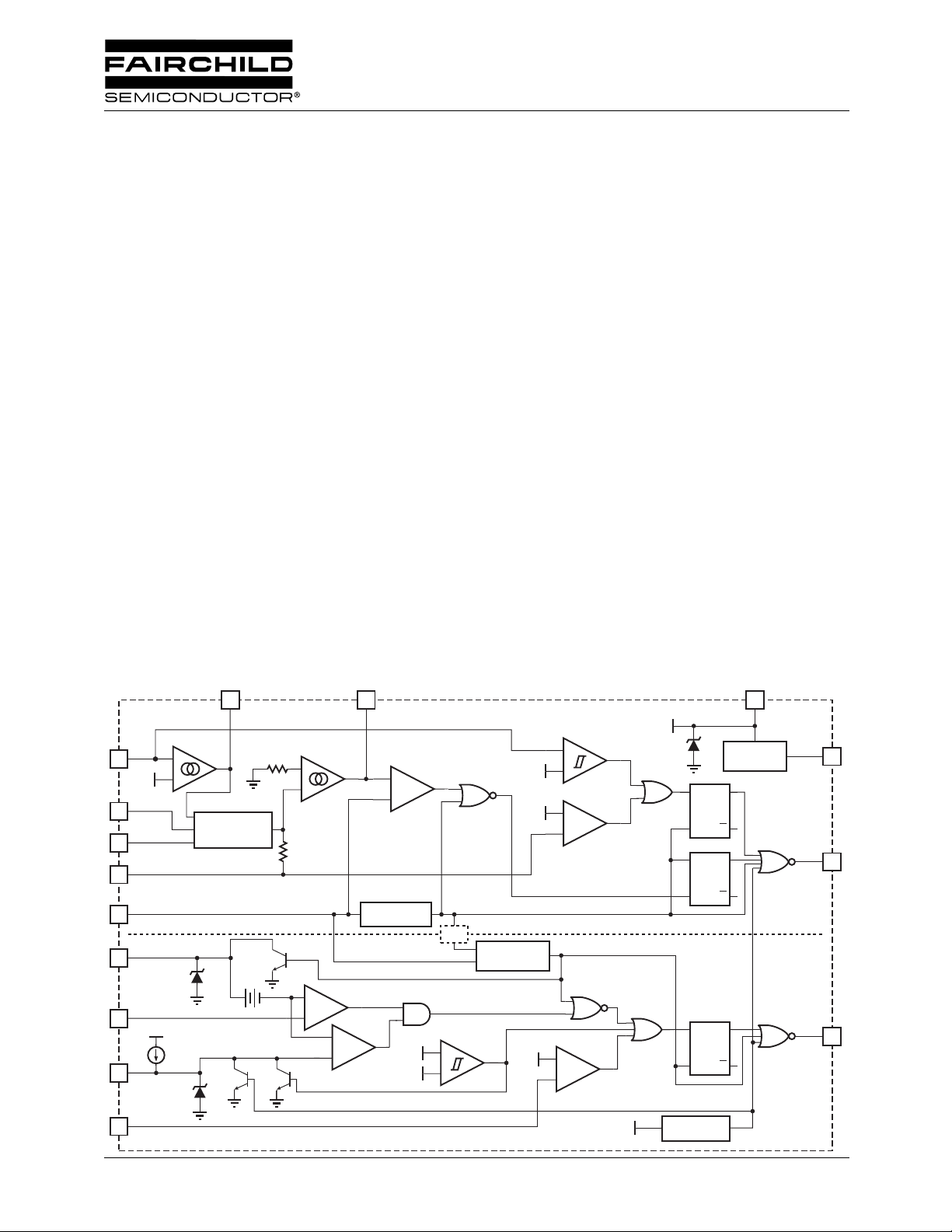
Block Diagram
15
2
4
3
7
8
6
5
9
V
FB
2.5V
I
AC
V
RMS
I
SENSE
RAMP 1
RAMP 2
V
DC
V
CC
SS
DC I
LIMIT
VEA
–
+
8V
50µA
8V
16
VEAO
GAIN
MODULATOR
1.25V
3.5kΩ
IEA
+
–
3.5kΩ
–
+
1
IEAO
(-2 VERSION ONLY)
–
+
POWER FACTOR CORRECTOR
+
–
OSCILLATOR
V
2.5V
x 2
–
FB
+
PULSE WIDTH MODULATOR
General Description
The ML4824 is a controller for power factor corrected,
switched mode power supplies. Power Factor Correction
(PFC) allows the use of smaller, lower cost bulk capacitors,
reduces power line loading and stress on the switching FETs,
and results in a power supply that fully complies with
IEC1000-2-3 specification. The ML4824 includes circuits
for the implementation of a leading edge, average current,
“boost” type power factor correction and a trailing edge,
pulse width modulator (PWM).
The device is av ailable in two versions; the ML4824-1 (f
= f
) and the ML4824-2 (f
PFC
switching frequency of the PWM allows the user to design
with smaller output components while maintaining the best
operating frequency for the PFC. An over-voltage comparator shuts down the PFC section in the event of a sudden
decrease in load. The PFC section also includes peak current
limiting and input voltage brown-out protection. The PWM
section can be operated in current or voltage mode at up to
250kHz and includes a duty cycle limit to prevent transformer saturation.
OVP
+
2.7V
–
–1V
+
–
PFC I
LIMIT
DUTY CYCLE
LIMIT
VIN OK
1V
–
+
DC I
LIMIT
V
CCZ
V
CCZ
13.5V
PWM
= 2 x f
SRQ
SRQ
SRQ
UVLO
). Doubling the
PFC
13
V
CC
7.5V
REFERENCE
Q
Q
PWM OUT
Q
PFC OUT
V
REF
PWM
14
12
11
REV. 1.0.6 11/7/03
Page 2
ML4824 PRODUCT SPECIFICATION
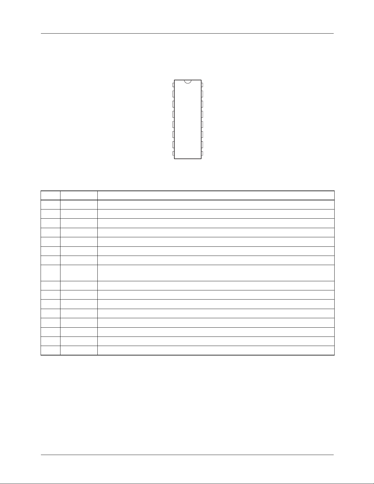
Pin Configuration
ML4824
16-Pin PDIP (P16)
16-Pin Wide SOIC (S16W)
IEAO
I
AC
I
SENSE
V
RMS
SS
V
DC
RAMP 1
RAMP 2
1
2
3
4
5
6
7
8
TOP VIEW
16
VEAO
15
V
FB
14
V
REF
13
V
CC
12
PFC OUT
11
PWM OUT
10
GND
9
DC I
LIMIT
Pin Description
PIN NAME FUNCTION
1 IEAO PFC transconductance current error amplifier output
2I
3I
4V
AC
SENSE
RMS
5 SS Connection point for the PWM soft start capacitor
6V
DC
7 RAMP 1 Oscillator timing node; timing set by R
8 RAMP 2 When in current mode, this pin functions as as the current sense input; when in voltage
9 DC I
LIMIT
10 GND Ground
11 PWM OUT PWM driver output
12 PFC OUT PFC driver output
13 V
14 V
15 V
CC
REF
FB
16 VEAO PFC transconductance voltage error amplifier output
PFC gain control reference input
Current sense input to the PFC current limit comparator
Input for PFC RMS line voltage compensation
PWM voltage feedback input
C
T
T
mode, it is the PWM input from PFC output (feed forward ramp).
PWM current limit comparator input
Positive supply (connected to an internal shunt regulator)
Buffered output for the internal 7.5V reference
PFC transconductance voltage error amplifier input
2
REV. 1.0.6 11/7/03
Page 3
∆
∆
Ω
PRODUCT SPECIFICATION ML4824
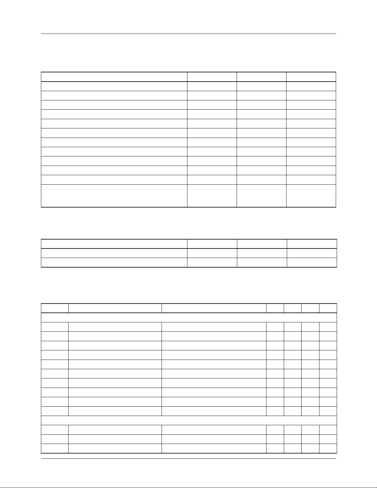
Absolute Maximum Ratings
Absolute maximum ratings are those values beyond which the device could be permanently damaged. Absolute maximum
ratings are stress ratings only and functional device operation is not implied.
Parameter Min. Max. Units
V
Shunt Regulator Current 55 mA
CC
I
Voltage on Any Other Pin GND – 0.3 V
I
I
Peak PFC OUT Current, Source or Sink 500 mA
Peak PWM OUT Current, Source or Sink 500 mA
PFC OUT, PWM OUT Energy Per Cycle 1.5 µJ
Junction Temperature 150 °C
Storage Temperature Range –65 150 °C
Lead Temperature (Soldering, 10 sec) 260 °C
Thermal Resistance ( θ
Plastic DIP
Plastic SOIC
Voltage –35 V
SENSE
+ 0.3 V
CCZ
REF
Input Current 10 mA
AC
)
JA
20 mA
80
105
°C/W
°C/W
Operating Conditions
Temperature Range
Parameter Min. Max. Units
ML4824CX 0 70 °C
ML4824IX –40 85 °C
Electrical Characteristics
Unless otherwise specified, I
Symbol Parameter Conditions Min. Typ. Max. Units
Voltage Error Amplifier
Input Voltage Range 0 7 V
Transconductance V
Feedback Reference Voltage 2.46 2.53 2.60 V
Input Bias Current Note 2 -0.3 –1.0 µA
Output High Voltage 6.0 6.7 V
Output Low Voltage 0.6 1.0 V
Source Current
Sink Current
Open Loop Gain 60 75 dB
Power Supply Rejection Ratio V
Current Error Amplifier
Input Voltage Range –1.5 2 V
Transconductance V
Input Offset Voltage 0 8 15 mV
= 25mA, R
CC
= 52.3k Ω , C
T
NON INV
V
IN
V
IN
CCZ
NON INV
= 470pF, T
T
= V
INV
= ±0.5V, V
= ±0.5V, V
- 3V < V
= V
INV
= Operating Temperature Range (Note 1)
A
, VEAO = 3.75V 50 85 120 µ
= 6V –40 –80 µA
OUT
= 1.5V 40 80 µA
OUT
< V
CC
, VEAO = 3.75V 130 195 310 µ
- 0.5V 60 75 dB
CCZ
Ω
REV. 1.0.6 11/7/03
3
Page 4

∆
∆
∆
ML4824 PRODUCT SPECIFICATION
Input Bias Current –0.5 –1.0 µA
Output High Voltage 6.0 6.7 V
Output Low Voltage 0.6 1.0 V
Source Current
Sink Current
V
= ±0.5V, V
IN
V
= ±0.5V, V
IN
= 6V –40 –90 µA
OUT
= 1.5V 40 90 µA
OUT
Open Loop Gain 60 75 dB
Power Supply Rejection Ratio V
CCZ
- 3V < V
CC
< V
- 0.5V 60 75 dB
CCZ
OVP Comparator
Threshold Voltage 2.6 2.7 2.8 V
Hysteresis 80 115 150 mV
PFC I
Comparator
LIMIT
Threshold Voltage –0.8 –1.0 –1.15 V
(PFC I
LIMIT
V
TH
- Gain
100 190 mV
Modulator Output)
Delay to Output 150 300 ns
DC I
Comparator
LIMIT
Threshold Voltage 0.97 1.02 1.07 V
Input Bias Current ±0.3 ±1 µA
Delay to Output 150 300 ns
V
OK Comparator
IN
Threshold Voltage 2.4 2.5 2.6 V
Hysteresis 0.8 1.0 1.2 V
Gain Modulator
Gain (Note 3) I
= 100µA, V
AC
I
= 50µA, V
AC
I
= 50µA, V
AC
I
= 100µA, V
AC
RMS
RMS
RMS
RMS
= V
= 0V 0.36 0.55 0.66
FB
= 1.2V, V
= 1.8V, V
= 3.3V, V
= 0V 1.20 1.80 2.24
FB
= 0V 0.55 0.80 1.01
FB
= 0V 0.14 0.20 0.26
FB
Bandwidth IAC = 100µA 10 MHz
Output Voltage I
= 250µA, V
AC
V
= 0V
FB
RMS
= 1.15V,
0.74 0.82 0.90 V
Oscillator
Initial Accuracy T
Voltage Stability V
= 25°C 717681kHz
A
CCZ
- 3V < V
CC
< V
- 0.5V 1 %
CCZ
Temperature Stability 2 %
Total Variation Line, Temp 68 84 kHz
Ramp Valley to Peak Voltage 2.5 V
Dead Time PFC Only 270 370 470 ns
C
T
4
REV. 1.0.6 11/7/03
Page 5
PRODUCT SPECIFICATION ML4824
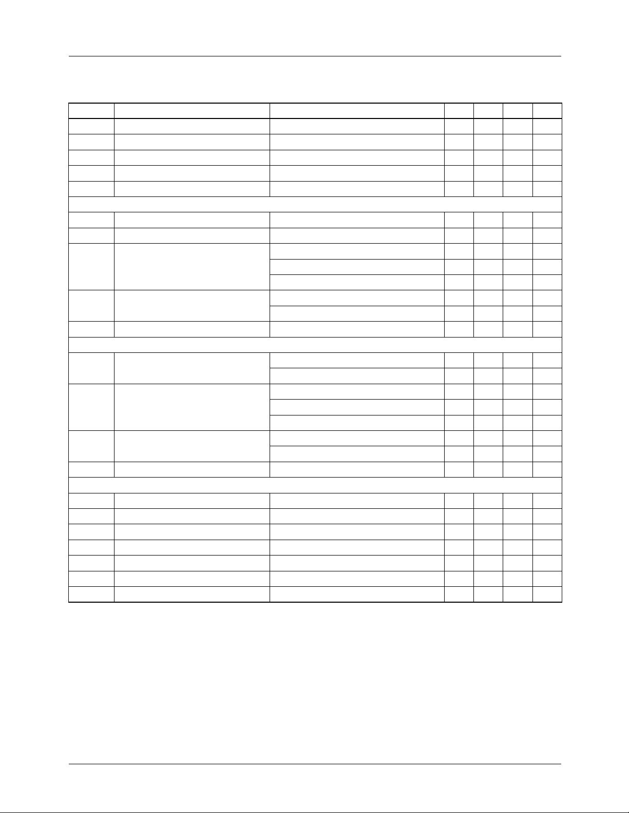
Electrical Characteristics (continued)
Unless otherwise specified, ICC = 25mA, RT = 52.3kΩ, CT = 470pF, TA = Operating Temperature Range (Note 1)
Symbol Parameter Conditions Min. Typ. Max. Units
Line Regulation V
Load Regulation 1mA < I(V
Temperature Stability 0.4 %
Total Variation Line, Load, Temp 7.35 7.65 V
Long Term Stability T
PFC
Minimum Duty Cycle V
Maximum Duty Cycle V
Output Low Voltage I
Output High Voltage I
Rise/Fall Time CL = 1000pF 50 ns
PWM
Duty Cycle Range ML4824-1 0-44 0-47 0-50 %
Output Low Voltage I
Output High Voltage I
Rise/Fall Time CL = 1000pF 50 ns
Supply
Shunt Regulator Voltage (V
V
Load Regulation 25mA < ICC < 55mA ±100 ±300 mV
CCZ
V
Total Variation Load, Temp 12.4 14.6 V
CCZ
) 12.8 13.5 14.4 V
CCZ
Start-up Current VCC = 11.8V, CL = 0 0.7 1.0 mA
Operating Current VCC < V
Undervoltage Lockout Threshold 12 13 14 V
Undervoltage Lockout Hysteresis 2.7 3.0 3.3 V
Notes
1. Limits are guaranteed by 100% testing, sampling, or correlation with worst-case test conditions.
2. Includes all bias currents to other circuits connected to the V
3. Gain = K x 5.3V; K = (I
GAINMOD
- I
OFFSET
) x IAC x (VEAO - 1.5V)-1.
- 3V < VCC < V
CCZ
) < 20mA 2 15 mV
REF
= 125˚C, 1000 Hours 5 25 mV
J
> 4.0V 0 %
IEAO
< 1.2V 90 95 %
IEAO
= -20mA 0.4 0.8 V
OUT
I
= -100mA 0.8 2.0 V
OUT
I
= 10mA, VCC = 8V 0.7 1.5 V
OUT
= 20mA 10 10.5 V
OUT
I
= 100mA 9.5 10 V
OUT
- 0.5V 2 10 mV
CCZ
ML4824-2 0-37 0-40 0-45 %
= -20mA 0.4 0.8 V
OUT
I
= -100mA 0.8 2.0 V
OUT
I
= 10mA, VCC = 8V 0.7 1.5 V
OUT
= 20mA 10 10.5 V
OUT
I
= 100mA 9.5 10 V
OUT
- 0.5V, CL = 0 16 19 mA
CCZ
pin.
FB
REV. 1.0.6 11/7/03 5
Page 6
ML4824 PRODUCT SPECIFICATION
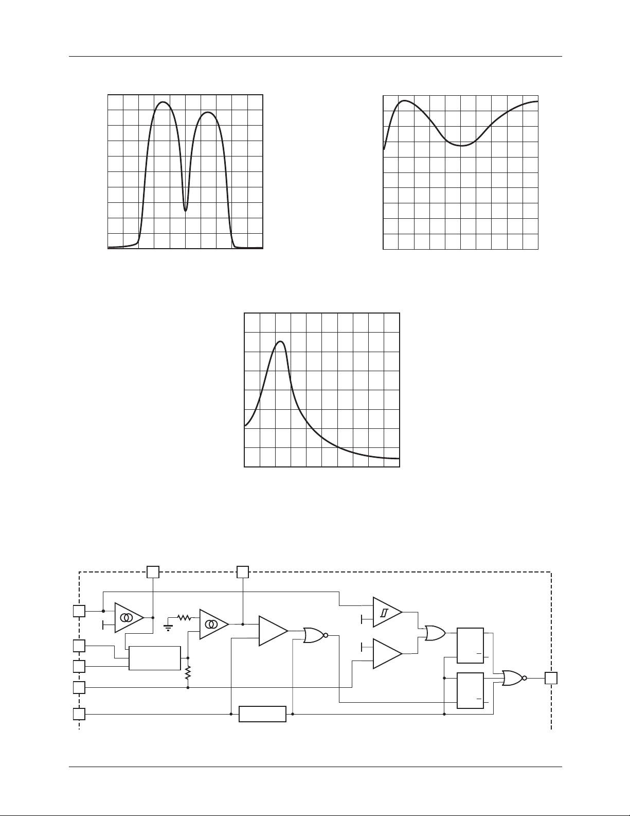
Typical Performance Characteristics
250
200
Ω
250
200
Ω
150
100
TRANSCONDUCTANCE (µ )
50
0
053
142
VFB (V)
Voltage Error Amplifier (VEA) Transconductance (g
VARIABLE GAIN BLOCK CONSTANT - K
400
300
200
100
0
053142
150
100
TRANSCONDUCTANCE (µ )
50
0
–500 5000
IEA INPUT VOLTAGE (mV)
)
m
V
RMS
Current Error Amplifier (IEA) Transconductance (g
(mV)
)
m
Gain Modulator Transfer Characteristic (K)
15
2
4
3
7
V
FB
2.5V
I
AC
V
RMS
I
SENSE
RAMP 1
VEAO
VEA
–
+
MODULATOR
16
GAIN
3.5kΩ
IEA
+
–
3.5kΩ
IEAO
1
+
–
OSCILLATOR
2.7V
–1V
OVP
+
–
+
–
PFC I
LIMIT
SRQ
SRQ
Q
PFC OUT
12
Q
Figure 1. PFC Section Block Diagram.
6 REV. 1.0.6 11/7/03
Page 7

PRODUCT SPECIFICATION ML4824
Functional Description
The ML4824 consists of an average current controlled,
continuous boost Power Factor Corrector (PFC) front end
and a synchronized Pulse Width Modulator (PWM) back
end. The PWM can be used in either current or voltage
mode. In voltage mode, feedforward from the PFC output
buss can be used to improve the PWM’s line regulation. In
either mode, the PWM stage uses conventional trailing-edge
duty cycle modulation, while the PFC uses leading-edge
modulation. This patented leading/trailing edge modulation
technique results in a higher useable PFC error amplifier
bandwidth, and can significantly reduce the size of the PFC
DC buss capacitor.
The synchronization of the PWM with the PFC simplifies the
PWM compensation due to the controlled ripple on the PFC
output capacitor (the PWM input capacitor). The PWM
section of the ML4824-1 runs at the same frequency as the
PFC. The PWM section of the ML4824-2 runs at twice the
frequency of the PFC, which allows the use of smaller PWM
output magnetics and filter capacitors while holding down
the losses in the PFC stage power components.
In addition to power factor correction, a number of protection features have been built into the ML4824. These include
soft-start, PFC over-voltage protection, peak current limiting, brown-out protection, duty cycle limit, and undervoltage lockout.
Power Factor Correction
Power factor correction makes a non-linear load look like a
resistive load to the AC line. For a resistor, the current drawn
from the line is in phase with and proportional to the line
voltage, so the power factor is unity (one). A common class
of non-linear load is the input of most power supplies, which
use a bridge rectifier and capacitive input filter fed from the
line. The peak-charging effect which occurs on the input
filter capacitor in these supplies causes brief high-amplitude
pulses of current to flow from the power line, rather than a
sinusoidal current in phase with the line voltage. Such
supplies present a power factor to the line of less than one
(i.e. they cause significant current harmonics of the power
line frequency to appear at their input). If the input current
drawn by such a supply (or any other non-linear load) can be
made to follow the input voltage in instantaneous amplitude,
it will appear resistive to the A C line and a unity po wer factor
will be achieved.
and back to zero. By forcing the boost converter to meet two
simultaneous conditions, it is possible to ensure that the
current which the converter draws from the power line
agrees with the instantaneous line voltage. One of these
conditions is that the output voltage of the boost converter
must be set higher than the peak value of the line voltage.
A commonly used value is 385VDC, to allow for a high line
of 270VAC
the converter is allowed to draw from the line at any given
instant must be proportional to the line voltage. The first of
these requirements is satisfied by establishing a suitable
voltage control loop for the converter, which in turn drives a
current error amplifier and switching output driver. The
second requirement is met by using the rectified AC line
voltage to modulate the output of the voltage control loop.
Such modulation causes the current error amplifier to
command a power stage current which varies directly with
the input voltage. In order to prevent ripple which will
necessarily appear at the output of the boost circuit (typically
about 10VAC on a 385V DC level) from introducing distortion back through the voltage error amplifier, the bandwidth
of the voltage loop is deliberately kept low. A final refinement is to adjust the overall gain of the PFC such to be
proportional to 1/V
of the system as the AC input voltage varies.
Since the boost converter topology in the ML4824 PFC is of
the current-averaging type, no slope compensation is
required.
. The other condition is that the current which
rms
2
, which linearizes the transfer function
IN
PFC Section
Gain Modulator
Figure 1 shows a block diagram of the PFC section of the
ML4824. The gain modulator is the heart of the PFC, as it is
this circuit block which controls the response of the current
loop to line voltage waveform and frequency, rms line
voltage, and PFC output voltage. There are three inputs to
the gain modulator. These are:
1. A current representing the instantaneous input voltage
(amplitude and waveshape) to the PFC. The rectified AC
input sine wave is converted to a proportional current
via a resistor and is then fed into the gain modulator at
IAC. Sampling current in this way minimizes ground
noise, as is required in high power switching power
conversion environments. The gain modulator responds
linearly to this current.
To hold the input current draw of a device drawing power
from the AC line in phase with and proportional to the input
voltage, a way must be found to prevent that device from
loading the line except in proportion to the instantaneous line
voltage. The PFC section of the ML4824 uses a boost-mode
DC-DC converter to accomplish this. The input to the
converter is the full wave rectified AC line voltage. No bulk
filtering is applied following the bridge rectifier, so the
input voltage to the boost converter ranges (at twice line
frequency) from zero volts to the peak value of the AC input
REV. 1.0.6 11/7/03 7
2. A voltage proportional to the long-term rms AC line
voltage, derived from the rectified line voltage after
scaling and filtering. This signal is presented to the gain
modulator at V
inversely proportional to V
low values of V
takes over, to limit power dissipation of the circuit
components under heavy brownout conditions). The
relationship between V
illustrated in the Typical Performance Characteristics.
. The gain modulator’s output is
RMS
where special gain contouring
RMS
RMS
2
(except at unusually
RMS
and gain is called K, and is
Page 8
ML4824 PRODUCT SPECIFICATION
3. The output of the voltage error amplifier, VEAO. The
gain modulator responds linearly to variations in this
voltage.
V
REF
The output of the gain modulator is a current signal, in the
form of a full wave rectified sinusoid at twice the line
frequency. This current is applied to the virtual-ground
(negative) input of the current error amplifier. In this way
the gain modulator forms the reference for the current error
loop, and ultimately controls the instantaneous current draw
of the PFC from the power line. The general form for the
output of the gain modulator is:
I
GAINMOD
IACVEAO×
--------------------------------
V
RMS
2
1V×≅
(1)
More exactly, the output current of the gain modulator is
PFC
OUTPUT
15
2
4
3
V
FB
2.5V
I
AC
V
RMS
I
SENSE
VEAO
VEA
–
+
MODULATOR
16
GAIN
1
IEAO
IEA
+
–
+
–
given by:
I
GAINMOD
where K is in units of V
K VEAO 1.5V–()× IAC×≅
-1
.
Note that the output current of the gain modulator is limited
to ≅ 200µA.
Current Error Amplifier
The current error amplifier’s output controls the PFC duty
cycle to keep the average current through the boost inductor
a linear function of the line voltage. At the inverting input to
the current error amplifier, the output current of the gain
modulator is summed with a current which results from a
negative voltage being impressed upon the I
(current into I
voltage on I
SENSE
SENSE
≅ V
/3.5kΩ). The negative
SENSE
represents the sum of all currents flowing
SENSE
in the PFC circuit, and is typically derived from a current
sense resistor in series with the negative terminal of the input
bridge rectifier. In higher power applications, two current
transformers are sometimes used, one to monitor the ID of
the boost MOSFET(s) and one to monitor the IF of the boost
diode. As stated above, the inverting input of the current
error amplifier is a virtual ground. Given this fact, and the
arrangement of the duty cycle modulator polarities internal
to the PFC, an increase in positive current from the gain
modulator will cause the output stage to increase its duty
cycle until the voltage on I
is adequately negative to
SENSE
cancel this increased current. Similarly, if the gain modulator’s output decreases, the output duty c ycle will decrease, to
achieve a less negative voltage on the I
SENSE
pin.
pin
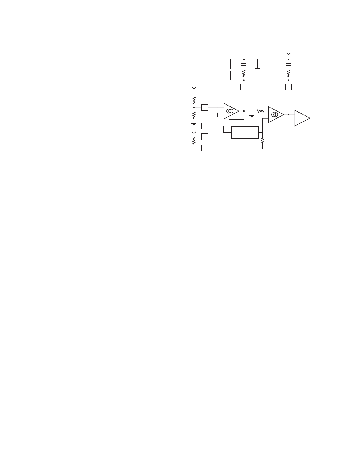
Figure 2. Compensation Network Connections for the
Overvoltage Protection
Voltage and Current Error Amplifiers
The OVP comparator serves to protect the power circuit
from being subjected to excessive v oltages if the load should
suddenly change. A resistor divider from the high voltage
DC output of the PFC is fed to VFB. When the voltage on
VFB exceeds 2.7V, the PFC output driver is shut down. The
PWM section will continue to operate. The OVP comparator
has 125mV of hysteresis, and the PFC will not restart until
the voltage at VFB drops below 2.58V. The VFB should be
set at a level where the active and passive external power
components and the ML4824 are within their safe operating
voltages, but not so low as to interfere with the boost v oltage
regulation loop.
Error Amplifier Compensation
The PWM loading of the PFC can be modeled as a negative
resistor; an increase in input voltage to the PWM causes a
decrease in the input current. This response dictates the
proper compensation of the two transconductance error
amplifiers. Figure 2 shows the types of compensation
networks most commonly used for the voltage and current
error amplifiers, along with their respective return points.
The current loop compensation is returned to V
REF
to
produce a soft-start characteristic on the PFC: as the
reference voltage comes up from zero volts, it creates a
differentiated voltage on IEAO which prevents the PFC
from immediately demanding a full duty cycle on its boost
converter.
Cycle-By-Cycle Current Limiter
The I
pin, as well as being a part of the current
SENSE
feedback loop, is a direct input to the cycle-by-cycle current
limiter for the PFC section. Should the input voltage at this
pin ever be more negative than -1V, the output of the PFC
will be disabled until the protection flip-flop is reset by the
clock pulse at the start of the next PFC power cycle.
There are two major concerns when compensating the
voltage loop error amplifier; stability and transient response.
Optimizing interaction between transient response and
stability requires that the error amplifier’s open-loop
crossover frequency should be 1/2 that of the line frequency,
or 23Hz for a 47Hz line (lowest anticipated international
power frequency). The gain vs. input voltage of the
8 REV. 1.0.6 11/7/03
Page 9

PRODUCT SPECIFICATION ML4824
ML4824’s voltage error amplifier has a specially shaped
nonlinearity such that under steady-state operating conditions the transconductance of the error amplifier is at a local
minimum. Rapid perturbations in line or load conditions will
cause the input to the voltage error amplifier (V
) to devi-
FB
ate from its 2.5V (nominal) value. If this happens, the
transconductance of the voltage error amplifier will increase
significantly, as shown in the Typical Performance Characteristics. This raises the gain-bandwidth product of the voltage loop, resulting in a much more rapid voltage loop
response to such perturbations than would occur with a conventional linear gain characteristic.
The current amplifier compensation is similar to that of the
voltage error amplifier with the exception of the choice of
crossover frequency. The crossover frequency of the current
amplifier should be at least 10 times that of the voltage
amplifier, to prevent interaction with the voltage loop. It
should also be limited to less than 1/6th that of the switching
frequency, e.g. 16.7kHz for a 100kHz switching frequency.
There is a modest degree of gain contouring applied to the
transfer characteristic of the current error amplifier, to
increase its speed of response to current-loop perturbations.
However, the boost inductor will usually be the dominant
factor in overall current loop response. Therefore, this contouring is significantly less marked than that of the voltage
error amplifier. This is illustrated in the Typical Performance
Characteristics.
For more information on compensating the current and
voltage control loops, see Application Notes 33 and 34.
Application Note 16 also contains valuable information for
the design of this class of PFC.
Oscillator (RAMP 1)
The oscillator frequency is determined by the values of RT
and CT, which determine the ramp and off-time of the
oscillator output clock:
f
OSC
-------------------------------------------------- -=
t
RAMPtDEADTIME
1
+
(2)
The deadtime of the oscillator is derived from the following
equation:
1.25–
V
REF
at V
t
RAMP
REF
t
RAMP
CTRT× In
= 7.5V:
CTRT× 0.51×=
------------------------------- -
×=
V
3.75–
REF
(3)
The deadtime of the oscillator may be determined using:
2.5V
t
DEADTIME
----------------- -
5.1mA
The deadtime is so small (t
C
× 490 CT×==
T
>> t
RAMP
DEADTIME
(4)
) that the
operating frequency can typically be approximated by:
f
OSC
1
----------------=
t
RAMP
(5)
EXAMPLE:
For the application circuit shown in the data sheet, with the
oscillator running at:
==
f
t
100kHz
OSC
RAMPCTRT
× 0.51× 110
1
---------------t
RAMP
5–
×==
Solving for RT x CT yields 2 x 10⁻⁴. Selecting standard
components values, CT = 470pF, and RT = 41.2kΩ.
The deadtime of the oscillator adds to the Maximum PWM
Duty Cycle (it is an input to the Duty Cycle Limiter). With
zero oscillator deadtime, the Maximum PWM Duty Cycle is
typically 45%. In many applications, care should be taken
that CT not be made so large as to extend the Maximum
Duty Cycle beyond 50%. This can be accomplished by using
a stable 470pF capacitor for CT.
PWM SECTION
Pulse Width Modulator
The PWM section of the ML4824 is straightforward, but
there are several points which should be noted. Foremost
among these is its inherent synchronization to the PFC
section of the device, from which it also derives its basic
timing (at the PFC frequency in the ML4824-1, and at twice
the PFC frequency in the ML4824-2). The PWM is capable
of current-mode or voltage mode operation. In current-mode
applications, the PWM ramp (RAMP 2) is usually derived
directly from a current sensing resistor or current transformer in the primary of the output stage, and is thereby
representative of the current flowing in the con v erter’ s output
stage. DC I
limiting, is typically connected to RAMP 2 in such applications. For voltage-mode operation or certain specialized
applications, RAMP 2 can be connected to a separate RC
timing network to generate a voltage ramp against which
VDC will be compared. Under these conditions, the use of
voltage feedforward from the PFC buss can assist in line
regulation accuracy and response. As in current mode
operation, the DC I
overcurrent protection.
No voltage error amplifier is included in the PWM stage of
the ML4824, as this function is generally performed on the
output side of the PWM’s isolation boundary. To facilitate
the design of optocoupler feedback circuitry, an offset has
been built into the PWM’ s RAMP 2 input which allo ws VDC
to command a zero percent duty cycle for input voltages
below 1.25V.
PWM Current Limit
The DC I
current limiter for the PWM section. Should the input
voltage at this pin ever exceed 1V, the output of the PWM
will be disabled until the output flip-flop is reset by the clock
pulse at the start of the next PWM power cycle.
, which provides cycle-by-cycle current
LIMIT
input is used for output stage
LIMIT
pin is a direct input to the cycle-by-cycle
LIMIT
REV. 1.0.6 11/7/03 9
Page 10
ML4824 PRODUCT SPECIFICATION
VIN OK Comparator
The V
and inhibits the PWM if this voltage on V
OK comparator monitors the DC output of the PFC
IN
is less than
FB
its nominal 2.5V. Once this voltage reaches 2.5V, which
corresponds to the PFC output capacitor being charged to its
rated boost voltage, the soft-start begins.
PWM Control (RAMP 2)
When the PWM section is used in current mode, RAMP 2 is
generally used as the sampling point for a voltage representing the current in the primary of the PWM’s output transformer, derived either by a current sensing resistor or a
current transformer. In voltage mode, it is the input for a
ramp voltage generated by a second set of timing components (R
RAMP2
, C
), which will have a minimum
RAMP2
value of zero volts and should have a peak value of approximately 5V. In voltage mode operation, feedforward from the
PFC output buss is an excellent way to derive the timing
ramp for the PWM stage.
Soft Start
Start-up of the PWM is controlled by the selection of the
external capacitor at SS. A current source of 50µA supplies
the charging current for the capacitor, and start-up of the
PWM begins at 1.25V. Start-up delay can be programmed by
the following equation::
50µA
--------------- -
C
SStDELAY
×=
1.25V
where CSS is the required soft start capacitance, and t
is the desired start-up delay.
It is important that the time constant of the PWM soft-start
allow the PFC time to generate sufficient output power for
the PWM section. The PWM start-up delay should be at least
5ms.
Solving for the minimum value of CSS:
50µA
C
SS
Caution should be exercised when using this minimum soft
start capacitance value because premature charging of the SS
capacitor and activation of the PWM section can result if
VFB is in the hysteresis band of the VIN OK comparator at
start-up. The magnitude of V
line voltage and nominal PFC output voltage. Typically, a
1.0µF soft start capacitor will allow time for V
out to reach their nominal values prior to activation of the
PWM section at line voltages between 90Vrms and
265Vrms.
GENERATING V
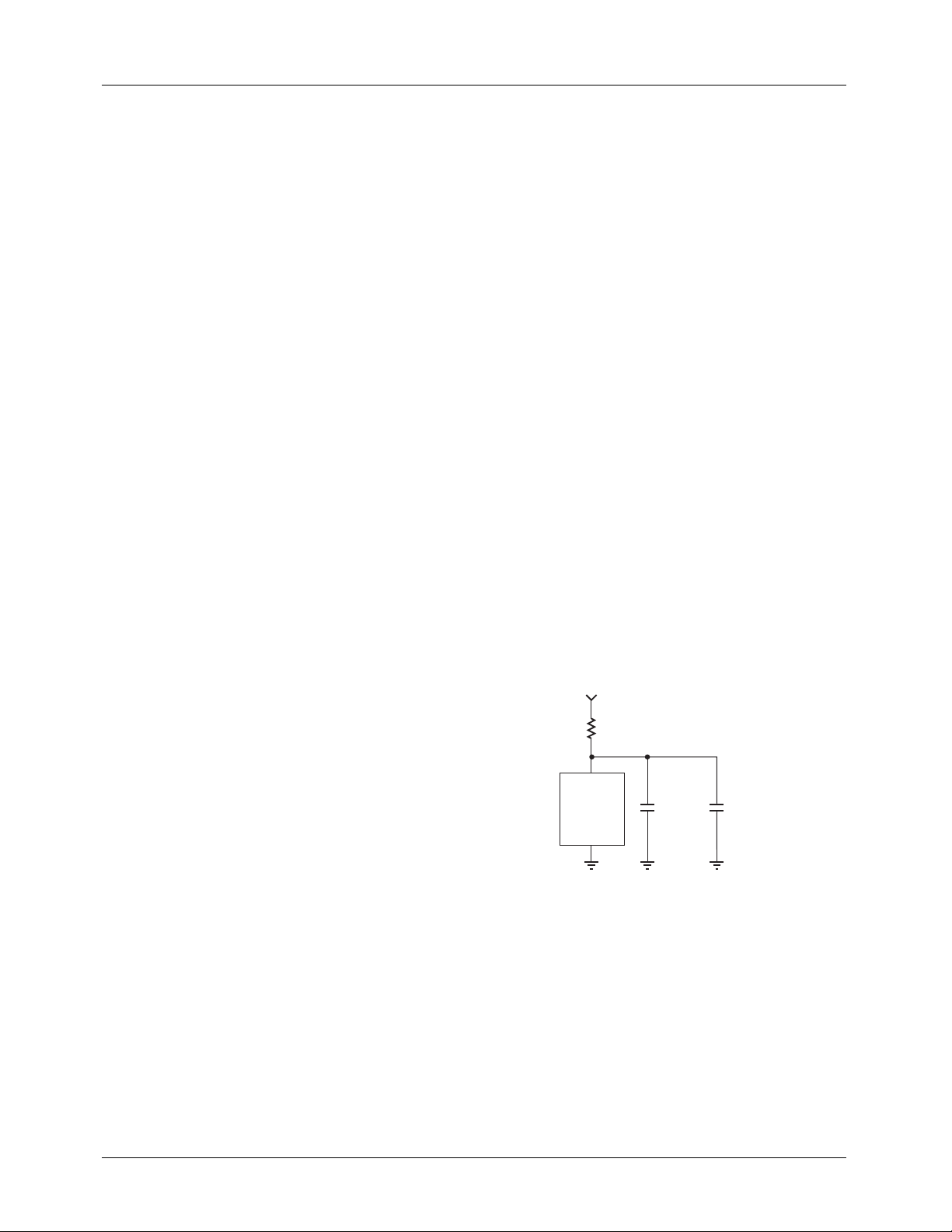
The ML4824 is a current-fed part. It has an internal shunt
voltage regulator, which is designed to regulate the voltage
internal to the part at 13.5V. This allows a low po wer dissipation while at the same time delivering 10V of gate drive at
the PWM OUT and PFC OUT outputs. It is important to
--------------- -
5ms
× 200nF==
1.25V
CC
at start-up is related both to
FB
FB
(6)
DELAY
and PFC
limit the current through the part to avoid overheating or
destroying it. This can be easily done with a single resistor in
series with the Vcc pin, returned to a bias supply of typically
18V to 20V. The resistor’s value must be chosen to meet the
operating current requirement of the ML4824 itself (19mA
max) plus the current required by the two gate driver outputs.
EXAMPLE:
With a V
of 20V, a VCC limit of 14.6V (max) and the
BIAS
ML4824 driving a total gate charge of 110nC at 100kHz
(e.g., 1 IRF840 MOSFET and 2 IRF830 MOSFETs), the
gate driver current required is:
I
GATEDRIVE
R
BIAS
100kHz 100nC× 11mA==
20V 14.6V–
-------------------------------------- - 180Ω==
19mA 11mA+
To check the maximum dissipation in the ML4824, find the
current at the minimum V
20V 12.4V–
I
-------------------------------- - 42.2mA==
CC
180Ω
(12.4V)::
CC
The maximum allowable ICC is 55mA, so this is an acceptable design.
The ML4824 should be locally bypassed with a 10nF and a
1µF ceramic capacitor. In most applications, an electrolytic
capacitor of between 100µF and 330µF is also required
across the part, both for filtering and as part of the start-up
bootstrap circuitry.
V
BIAS
R
BIAS
V
CC
ML4824
GND
Figure 3. External Component Connections to V
10nF
CERAMIC
1µF
CERAMIC
Leading/Trailing Modulation
Conventional Pulse Width Modulation (PWM) techniques
employ trailing edge modulation in which the switch will
turn on right after the trailing edge of the system clock.
The error amplifier output voltage is then compared with the
modulating ramp. When the modulating ramp reaches the
level of the error amplifier output voltage, the switch will be
turned OFF . When the switch is ON, the inductor current will
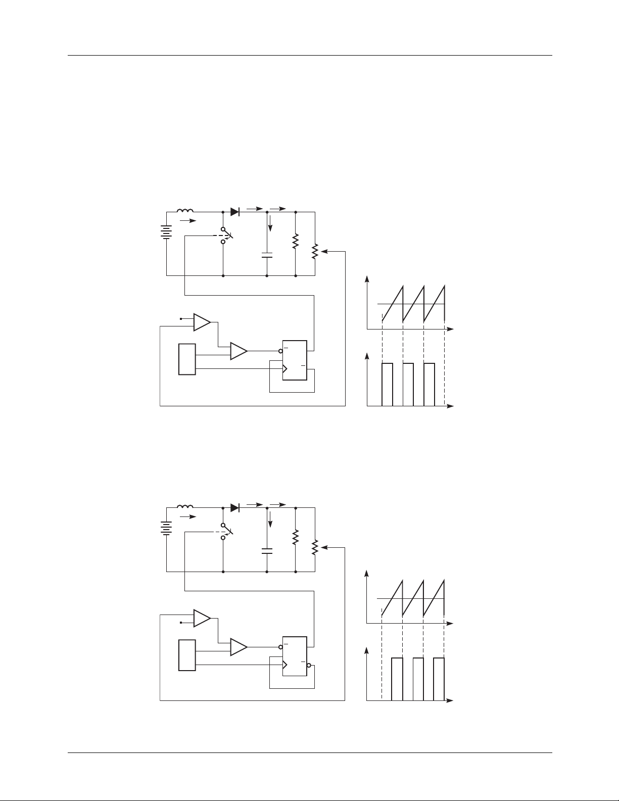
ramp up. The effective duty cycle of the trailing edge modulation is determined during the ON time of the switch. Figure
4 shows a typical trailing edge control scheme.
(7)
(8)
(9)
CC
10 REV. 1.0.6 11/7/03
Page 11
PRODUCT SPECIFICATION ML4824
In the case of leading edge modulation, the switch is turned
OFF right at the leading edge of the system clock. When the
modulating ramp reaches the level of the error amplifier
output voltage, the switch will be turned ON. The effective
duty-cycle of the leading edge modulation is determined
during the OFF time of the switch. Figure 5 shows a leading
edge control scheme.
+
DC
VIN
L1
I1
REF
OSC
U4
U3
+
EA
–
RAMP
CLK
SW2
SW1
+
–
U1
I3
I2
I4
C1
DFF
R
U2
D
CLK
One of the advantages of this control teccnique is that it
requires only one system clock. Switch 1 (SW1) turns off
and switch 2 (SW2) turns on at the same instant to minimize
the momentary “no-load” period, thus lowering ripple
voltage generated by the switching action. With such
synchronized switching, the ripple voltage of the first stage
is reduced. Calculation and evaluation have shown that the
120Hz component of the PFC’s output ripple voltage can be
reduced by as much as 30% using this method.
RL
RAMP
VEAO
TIME
Q
Q
VSW1
+
DC
VIN
Figure 4. Typical Trailing Edge Control Scheme.
L1
I1
REF
OSC
U4
U3
+
EA
–
RAMP
CLK
SW2
SW1
VEAO
+
–
CMP
U1
I3
I2
I4
RL
C1
DFF
R
Q
D
U2
Q
CLK
TIME
RAMP
VEAO
TIME
VSW1
TIME
Figure 5. Typical Leading Edge Control Scheme.
REV. 1.0.6 11/7/03 11
Page 12
ML4824 PRODUCT SPECIFICATION
TYPICAL APPLICATIONS
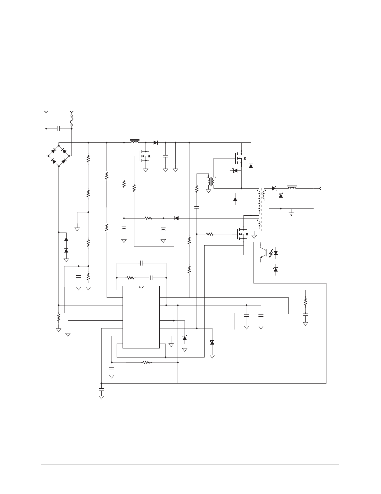
Figure 6 is the application circuit for a complete 100W
power factor corrected power supply, designed using the
methods and general topology detailed in Application
Note 33.
AC INPUT
85 TO 265VAC
C3
470nF
C2
470nF
F1
3.15A
R2A
357kΩ
R2B
357kΩ
D12
1A, 50V
D13
1A, 50V
C19
1µF
R1A
499kΩ
R1B
499kΩ
R3
75kΩ
R4
13kΩ
R27
39kΩ
C30
330µF
1
2
3
4
5
6
7
8
3.1mH
Q1
IRF840
R12
27kΩ
IEAO
I
AC
I
SENSE
V
RMS
SS
V
DC
RAMP 1
RAMP 2
L1
R21
22Ω
220pF
ML4824
8A, 600V
R28
180Ω
C7
1nF
VEAO
V
PFC OUT
PWM OUT
DC I
10nF
C12
10µF
C6
V
REF
V
GND
LIMIT
D1
CC
Q2
C4
D3
50V
100µF
R7A
178kΩ
R7B
178kΩ
C5
R15
3Ω
C20
1µF
R14
33Ω
IRF830
Q3
IRF830
L2
33µH
12VDC
16
15
FB
14
13
C13
100nF
C14
1µF
R11
750kΩ
12
11
10
9
D8
1A, 20V
D10
1A, 20V
C1
470nF
BR1
4A, 600V
R5
300mΩ
1W
C11
10nF
C18
470pF
R6
41.2kΩ
R10
6.2kΩ
Figure 6. 100W Power Factor Corrected Power Supply, Designed Using Micro Linear Application Note 33.
12 REV. 1.0.6 11/7/03
Page 13
PRODUCT SPECIFICATION ML4824
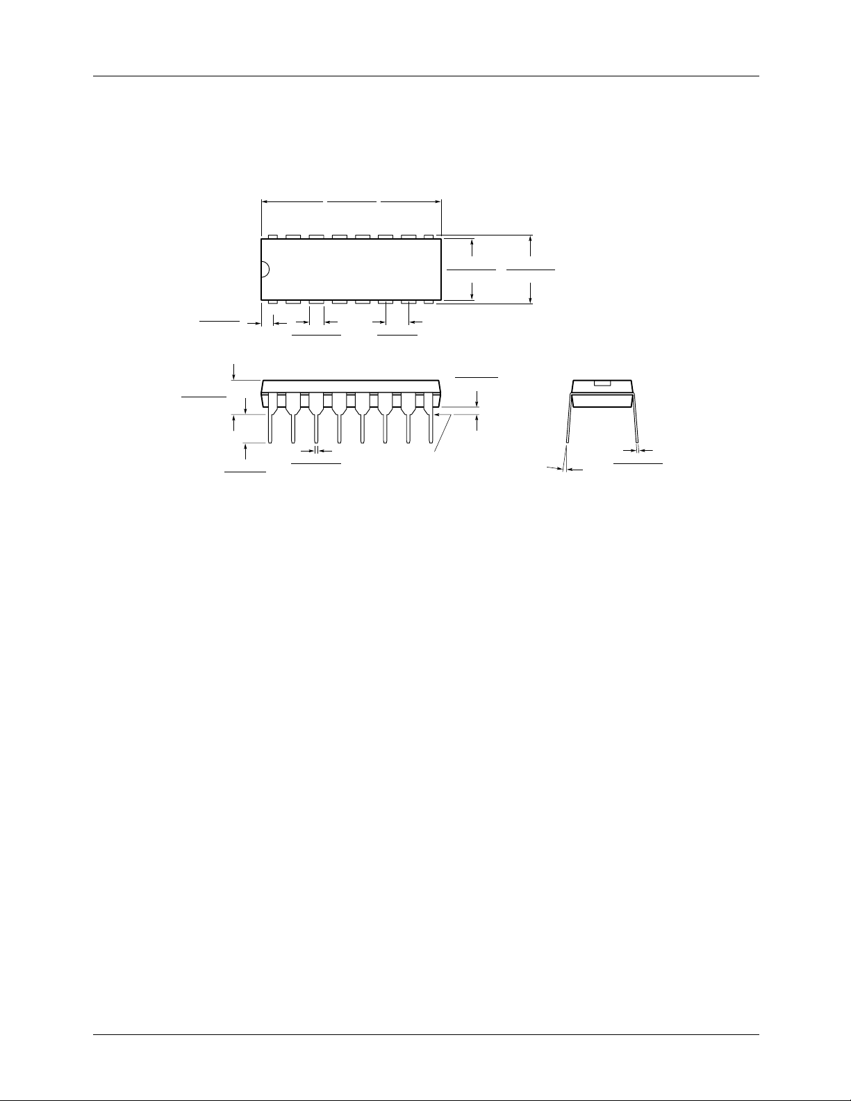
Mechanical Dimensions inches (millimeters)
Package: P16
16-Pin PDIP
0.740 - 0.760
(18.79 - 19.31)
16
0.02 MIN
(0.50 MIN)
(4 PLACES)
0.170 MAX
(4.32 MAX)
0.125 MIN
(3.18 MIN)
PIN 1 ID
1
0.055 - 0.065
(1.40 - 1.65)
0.016 - 0.022
(0.40 - 0.56)
0.100 BSC
(2.54 BSC)
SEATING PLANE
0.240 - 0.260
(6.09 - 6.61)
0.015 MIN
(0.38 MIN)
0.295 - 0.325
(7.49 - 8.26)
0° - 15°
0.008 - 0.012
(0.20 - 0.31)
REV. 1.0.6 11/7/03 13
Page 14
ML4824 PRODUCT SPECIFICATION
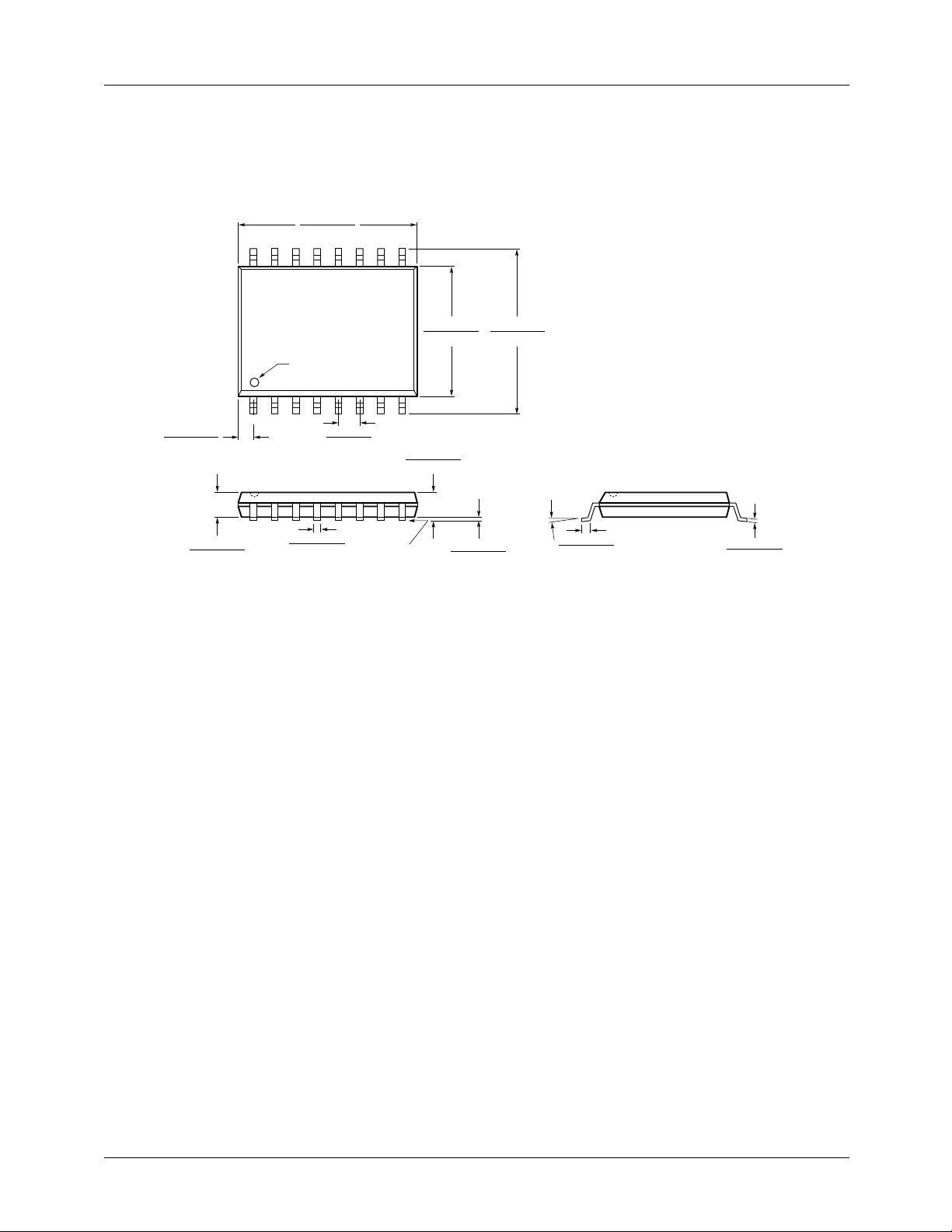
Mechanical Dimensions inches (millimeters)
Package: S16W
16-Pin Wide SOIC
0.400 - 0.414
16
(10.16 - 10.52)
0.024 - 0.034
(0.61 - 0.86)
(4 PLACES)
0.090 - 0.094
(2.28 - 2.39)
1
PIN 1 ID
0.050 BSC
(1.27 BSC)
0.012 - 0.020
(0.30 - 0.51)
0.291 - 0.301
(7.39 - 7.65)
0.095 - 0.107
(2.41 - 2.72)
SEATING PLANE
0.398 - 0.412
(10.11 - 10.47)
0.005 - 0.013
(0.13 - 0.33)
0° - 8°
0.022 - 0.042
(0.56 - 1.07)
0.009 - 0.013
(0.22 - 0.33)
14 REV. 1.0.6 11/7/03
Page 15

ML4824 PRODUCT SPECIFICATION
Ordering Information
Part Number PWM Frequency Temperature Range Package
ML4824CP1 1 x PFC 0°C to 70°C 16-Pin PDIP (P16)
ML4824CP2 2 x PFC 0°C to 70°C 16-Pin PDIP (P16)
ML4824CS1 1 x PFC 0°C to 70°C 16-Pin Wide SOIC (S16W)
ML4824CS2 2 x PFC 0°C to 70°C 16-Pin Wide SOIC (S16W)
ML4824IP1 1 x PFC –40°C to 85°C 16-Pin PDIP (P16)
ML4824IS1 1 x PFC –40°C to 85°C 16-Pin Wide SOIC (S16W)
ML4824IS2 2 x PFC –40°C to 85°C 16-Pin Wide SOIC (S16W)
DISCLAIMER
FAIRCHILD SEMICONDUCTOR RESERVES THE RIGHT TO MAKE CHANGES WITHOUT FURTHER NOTICE TO
ANY PRODUCTS HEREIN TO IMPROVE RELIABILITY, FUNCTION OR DESIGN. FAIRCHILD DOES NOT ASSUME
ANY LIABILITY ARISING OUT OF THE APPLICATION OR USE OF ANY PRODUCT OR CIRCUIT DESCRIBED HEREIN;
NEITHER DOES IT CONVEY ANY LICENSE UNDER ITS PATENT RIGHTS, NOR THE RIGHTS OF OTHERS.
LIFE SUPPORT POLICY
FAIRCHILD’S PRODUCTS ARE NOT AUTHORIZED FOR USE AS CRITICAL COMPONENTS IN LIFE SUPPORT DEVICES
OR SYSTEMS WITHOUT THE EXPRESS WRITTEN APPROVAL OF THE PRESIDENT OF FAIRCHILD SEMICONDUCTOR
CORPORATION. As used herein:
1. Life support devices or systems are devices or systems
which, (a) are intended for surgical implant into the body,
or (b) support or sustain life, and (c) whose failure to
perform when properly used in accordance with
instructions for use provided in the labeling, can be
reasonably expected to result in a significant injury of the
user.
www.fairchildsemi.com
2. A critical component in any component of a life support
device or system whose failure to perform can be
reasonably expected to cause the failure of the life support
device or system, or to affect its safety or effectiveness.
11/7/03 0.0m 003
© 2003 Fairchild Semiconductor Corporation
Stock#DS30004824
 Loading...