

Page 1

www.fairchildsemi.com
ML4821
Power Factor Controller
Features
• Average current sensing for lowest possible harmonic
distortion
• Average line compensation with brown-out control
• Precision buffered 5V reference
• 1A peak current totem-pole output drive
• Overvoltage comparator eliminates output “runaway” due
to load removal
• Wide common mode range in current sense comparators
for better noise immunity
• Large oscillator amplitude for better noise immunity
• Output driver internally limited to 17V
• “Sleep mode” shutdown input
Block Diagram
General Description
The ML4821 provides complete control for a “boost” type
power factor correction system using the average current
sensing method. Special care has been taken in the design of
the ML4821 to increase system noise immunity. The circuit
includes a precision reference, gain modulator, average
current error amplifier, output error amplifier, over-voltage
protection comparator, shutdown logic, as well as a high
current output. In addition, start-up is simplified by an undervoltage lockout circuit.
In a typical application, the ML4821 controls the AC input
current by adjusting the pulse width of the output MOSFET.
This modulates the line current so that its shape conforms to
the shape of the input voltage. The reference for the current
regulator is a product of the sinusoidal line voltage times the
output of the error amplifier which is regulating the output
DC voltage. Average line voltage compensation is provided
in the gain modulator to ensure constant loop gain over a
wide input voltage range. This compensation includes a
special “brown-out” control which reduces output power
below 90V RMS input.
OVP
11
I
LIM
1
IA OUT
2
IA–
3
IA+
4
I
SINE
5
V
RMS
8
EA OUT
6
EA–
7
SOFT START
9
+
V
REF
–
+
–
+
OUT
GAIN
MODULATOR
–
V
REF
+
–
–
+
V
REF
0.7V
+
–
R
S
Q
OSC
SLEEP
UNDER
VOLTAGE
LOCKOUT
V
LIMIT
17V
V
REF
GND
V
OUT
PGND
SYNC
16
18
CC
15
14
13
R
T
12
10
C
T
17
REV. 1.0.2 6/19/01
Page 2

ML4821 PRODUCT SPECIFICATION
Pin Connection
18-Pin PDIP (P18) 20-Pin SOIC (S20)
SOFT START
Pin Description
Pin Number
11I
2 2 IA OUT Output and compensation node of the average current error amplifier
33IA– Inverting input of the average current error amplifier
4 4 IA+ Non-Inverting input of the average current error amplifier and output of the
55I
6 6 EA OUT Output of output voltage error amplifier
7 7 INV Inverting input to error amplifier
88V
9 9 SOFT
10 12 SYNC Oscillator synchronization input
11 13 OVP Inhibits output pulses when the voltage at this pin exceeds 5V. Also,
12 14 R
13 15 PWR
14 16 OUT High current totem pole output
15 17 V
16 18 V
17 19 C
18 20 GND Analog signal ground
I
LIM
IA OUT
IA–
IA+
I
SINE
EA OUT
EA–
V
RMS
1
2
3
4
5
6
7
8
9
TOP VIEW
Name Function18-Pin DIP 20-Pin SOIC
LIM
SINE
RMS
START
GND
CC
REF
18
GND
17
C
T
V
16
REF
V
15
CC
OUT
14
13
PGND
12
R
T
OVP
11
10
SYNC
I
LIM
IA OUT
IA–
IA+
I
SINE
EA OUT
EA–
V
RMS
SOFT START
N/C
1
2
3
4
5
6
7
8
9
10
20
19
18
17
16
15
14
13
12
11
GND
C
T
V
REF
V
CC
OUT
PGND
R
T
OVP
SYNC
N/C
TOP VIEW
Peak cycle-by-cycle current limit input
gain modulator
Gain modulator input
Input for average line voltage compensation
Normally connected to soft start capacitor
when the voltage at this pin is less than 0.7V, the IC goes into low current
shut-down mode.
Timing resistor for the oscillator
T
Return for the high current totem pole output
Positive supply for the IC
Buffered output for the 5V voltage reference
Timing capacitor for the oscillator.
T
2
REV. 1.0.2 6/19/01
Page 3

PRODUCT SPECIFICATION ML4821
Absolute maximum ratings
Absolute maximum ratings are those values beyond which the device could be permanently damaged. Absolute maximum
ratings are stress ratings only and functional device operation is not implied.
Parameter Min Max Units
Supply Current (I
OUT Current, Source or Sink 1.0 A
Output Energy (capacitive load per cycle) 5 µJ
I
Input Current 1.2 mA
SINE
EA OUT Source Current 50 mA
Oscillator Charge Current 2 mA
Input Voltage GND –0.3V 5.5 V
Junction Temperature 150 °C
Storage Temperature Range –65 150 °C
Lead Temperature (Soldering 10 sec.) 260 °C
Thermal Resistance ( θ
Plastic DIP
Plastic SOIC
) 35 mA
CC
)
JA
75
95
°C/W
°C/W
Operating Conditions
Temperature Range Min Max Units
ML4821CX 0 70 °C
Electrical Characteristics
Unless otherwise specified, R
Parameter Conditions Min. Typ. Max. Units
Oscillator
Initial accuracy T
Voltage stability 12V < V
Temperature stability 2 %
Total Variation Line, Temperature 85 115 kHz
Ramp Valley to Peak 4.7 5.2 5.6 V
R
Voltage 4.8 5.0 5.2 V
T
Discharge Current C
SYNC Input Threshold 1.5 2.0 3.0 V
Reference
Output Voltage T
Line regulation 12V < V
Load regulation 1mA < I
Temperature stability .4 %
Total Variation line, load, temp 4.9 5.1 V
Output Noise Voltage 10Hz to 10kHz 50 µV
Long Term Stability T
Short Circuit Current V
= 6.2k Ω , C
T
= 720pF, T
T
= 25°C 90 100 110 kHz
A
CC
= 2V, R
T
= 25°C, I
A
CC
O
= 125°C, 1000 hrs 5 25 mV
A
= 0V –30 –85 –180 mA
REF
= Operating Temperature Range, V
A
< 18V 1 %
= Open 7.8 8.4 9.3 mA
T
= 1mA 4.95 5.00 5.05 V
O
< 24V 2 10 mV
< 20mA 2 15 mV
= 15V (Notes 1 & 2).
CC
REV. 1.0.2 6/19/01
3
Page 4

ML4821 PRODUCT SPECIFICATION
Electrical Characteristics
Unless otherwise specified, R
= 6.2k Ω , C
T
(continued)
= 720pF, T
T
= Operating Temperature Range, V
A
= 15V (Notes 1 & 2).
CC
Parameter Conditions Min. Typ. Max. Units
Voltage Error Amplifier
Input Offset Voltage 0 –15 mV
Input Bias Current –50 –800 nA
Open Loop Gain 2 < EA OUT < 6V 60 75 dB
PSRR 12V < V
< 24V 70 100 dB
CC
Output Sink Current EA OUT = 4V, INV = 5.5V 300 500 µA
Output Source Current EA OUT
Output High Voltage I
Output Low Voltage I
PIN6
PIN6
= 4.0V, INV
= –5mA, V
= 4.8V –10 –30 mA
= 4.8V 7.0 7.5 V
PIN7
= 0, EA– = 5.5V 0 0.5 V
Unity Gain Bandwidth 1.0 MHz
Soft Start Charge Current V
= 4V –22 –38 –50 µA
PIN9
Current Error Amplifier
Input Offset Voltage –50 5mV
Input Bias Current –0.15 –1µA
Input Offset Current 400 nA
Open Loop Gain 2 < EA OUT < 7V 80 100 dB
PSRR 12V < V
Output Voltage Low I
Output Voltage High I
= 300µA 0 0.5 V
OL
= –10mA 7.0 7.5 V
OH
< 24V 65 85 dB
CC
Input Common Mode Range –0.3 2.5 V
Gain Modulator
Gain V
Output Current V
Output Current Limit V
I
Comparator
LIM
INV
V
INV
V
INV
V
INV
INV
INV
V
RMS
= 4.8V, V
= 4.8V, V
= 4.8V, V
= 4.8V, V
= 5.2V, V
= 4.8V, I
= 1.75V
= 0V
RMS
= 1.75V
RMS
= 2.6V
RMS
= 5.2V
RMS
= 5.2V –2 –4µA
RMS
= 500 µ A,
SINE
0.75
3.1
1.25
0.22
1.2
3.88
1.75
0.38
1.3
4.5
2.15
0.50
360 395 420 µA
Input Offset Voltage +15 mV
Input Bias Current –100 –200 µA
OVP Comparator
Input Offset Voltage Output Off –25 5 mV
Hysteresis Output On 85 105 130 mV
Input Bias Current –0.3 –3µA
Propagation Delay 150 ns
Shutdown Threshold 0.4 0.7 1.0 V
PWM Comparator
Input Common Mode Range 0 8 V
Propagation Delay 150 ns
4
REV. 1.0.2 6/19/01
Page 5
PRODUCT SPECIFICATION ML4821
Electrical Characteristics
Unless otherwise specified, R
= 6.2k Ω , C
T
(continued)
= 720pF, T
T
= Operating Temperature Range, V
A
= 15V (Notes 1 & 2).
CC
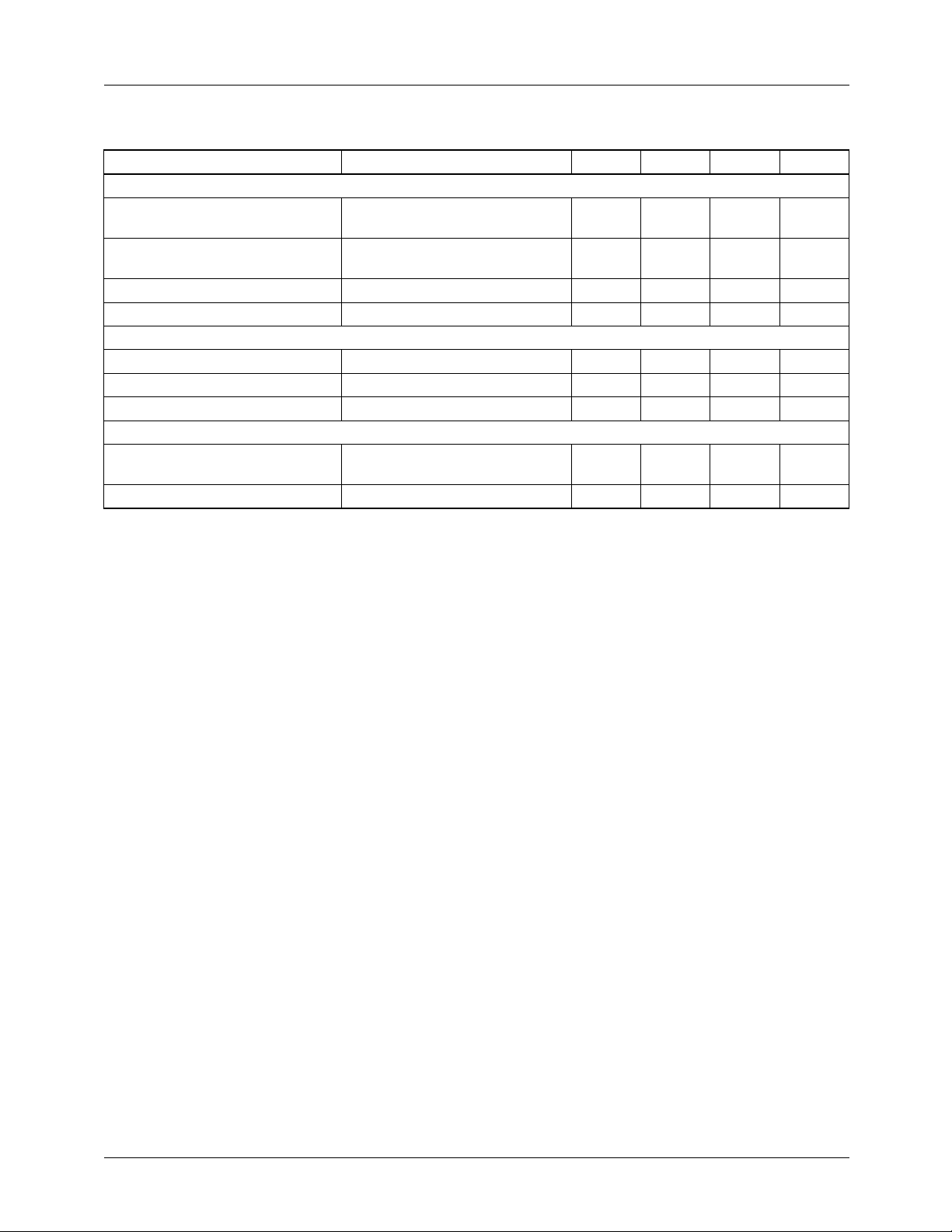
Parameter Conditions Min. Typ. Max. Units
Output
Output Voltage Low I
Output Voltage High I
Output Voltage Low in UVLO I
Output Rise/Fall Time C
= 20mA
OUT
I
= 200mA
OUT
= –20mA
OUT
I
= –200mA
OUT
= –5mA, V
OUT
= 1000pF 50 ns
L
= 8V 0.1 0.8 V
CC
13
12
0.1
1.6
13.5
13.4
0.4
2.4
Undervoltage Lockout
Start-up Threshold 14.5 16.5 V
Shut-Down Threshold 8.5 11.0 V
V
Good Threshold 4.4 V
REF
Supply
Supply Current Start-up, V
Operating, T
Internal Shunt Zener Voltage I
Notes:
1. Limits are guaranteed by 100% testing, sampling or correlation with worst case test conditions.
2. V
3. Gain Modulator gain is defined as:
is raised above the start-up threshold first to activate the IC, then returned to 15V
CC
= 35mA 25 27 35 V
CC
I
OUTIA+
------------------------
I
INEAOUT
= 14V, T
CC
= 25°C
A
= 25°C
A
0.6
26
1.2
32
V
V
V
V
mA
mA
REV. 1.0.2 6/19/01
5
Page 6
ML4821 PRODUCT SPECIFICATION
Functional Description
Oscillator
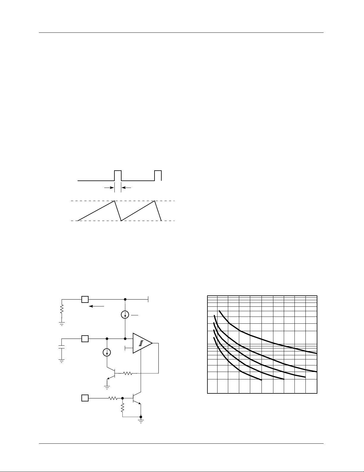
The ML4821 oscillator charges the external capacitor
connected to C
capacitor voltage reaches the upper threshold, the comparator changes state and the capacitor discharges to the lower
threshold through Q1.
The oscillator period can be described by the following
relationship:
T
OSC
= T
where:
T
RAMP
and:
T
DISCHARGE
CLOCK
RAMP PEAK
RAMP VALLEY
with a current equal to 2.5/RT. When the
T
+ T
RAMP
DISCHARGE
= C(Ramp Valley to Peak) ÷ (IRT/2)
= C(Ramp Valley to Pk) ÷ (8.4mA – IRT/2)
t
D
C
T
The ML4821 oscillator includes a SYNC input for synchronizing to an external frequency source. A positive pulse on
this pin of 2V (typ) resets the oscillators comparator and
initiates a discharge cycle for CT. The RT and CT component
values which set the ML4821 oscillator frequency should be
selected to produce a lower frequency than the external
frequency source.
VOLTAGE and Current ERROR Amplifiers
The ML4821 voltage error amplifier is a high open loop
gain, wide bandwidth amplifier with a class A output. The
soft start circuit controls the input to this amplifier for closed
loop soft start operation.
The current error amplifier (IA) is similar to the voltage error
amplifier but is designed for very low offsets to allow the
selection of a low value resistor for R
SENSE
.
Output Driver Stage
The ML4821 Output Driver is a 1A peak output high speed
totem pole circuit designed to quickly drive capacitive loads,
such as power MOSFET gates. The driver circuit’s output
voltage is internally limited to 17V.
Gain Modulator
The ML4821 gain modulator responds linearly to current
injected into the I
to voltage on the V
pin, the gain modulator enforces a power limit, or ”brownout protection”, upon the overall PFC circuit (Figures 6 and
7). The rectified line input sine wave is converted to a current
for the I
input via a dropping resistor. In this way, most
SINE
ground noise produces an insignificant effect on the reference to the PWM comparator. This gives the ML4821 a high
degree of immunity to the disturbances common in highpower switching circuits.
pin, and in an inverse-square fashion
SINE
pin. At very low voltages on the V
RMS
RMS
R
T
R
T
C
T
C
T
8.4mA
SYNC
I
R
T
Q1
2kΩ
1kΩ
V
REF
I
R
T
2
+
–
Q2
1000
100
FREQUENCY (kHz)
1nF
10
01020
150pF
RT (kΩ)
330pF
680pF
30 40
470pF
50
Figure 2. Oscillator Timing Resistance vs. Frequency
Figure 1. Oscillator Block Diagram
6 REV. 1.0.2 6/19/01
Page 7
PRODUCT SPECIFICATION ML4821
INV
7
+8V
–
EA OUT
S.S
+8V
9
+
V
REF
6.2kΩ
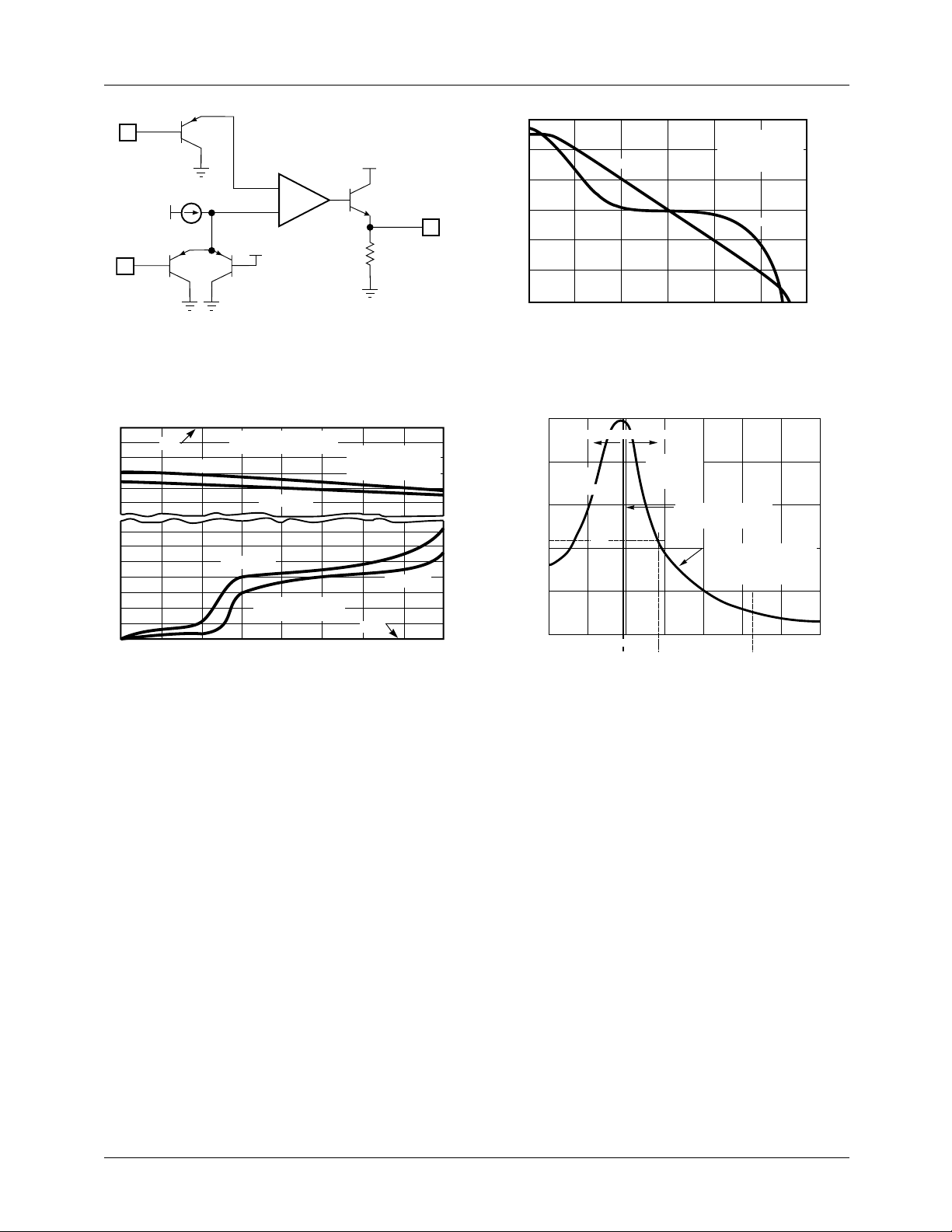
Figure 3. Error and Current Amplifier Configuration
0
.0
.0
.0
.0
.0
0
V
CC
TA = 25°C
0 200 400 600 800
, OUTPUT LOAD CURRENT (mA)
I
O
SATURATION
TA = –55°C
TA = –55°C
SOURCE
SINK
SATURATION
V
= 15V
CC
80µs PULSED
LOAD
TA = 25°C
GND
100
80
60
40
6
20
0
, OPEN-LOOP VOLTAGE GAIN (dB)
VOL
–20
A
10 100 1.0k 10k 100k 1.0M 10M
GAIN
f, FREQUENCY (Hz)
VCC = 15V
= 1.0V TO 5.0V
V
O
= 100kΩ
R
L
= 25°C
T
A
PHASE
0
–30
60
90
120
PHASE (DEGREES)
150
180
Figure 4. Error Amplifier Open-loop Gain and
Phase vs. Frequency.
0.5
OPERATING BOUNDRY
2
85VAC
DESIGN
FOR
NORMAL
OPERATIONS
THIS IS THE MINIMUM
OPERATING
VOLTAGE POINT
120VAC
V
RMS
THIS GAIN CURVE TAKES
OUT THE 1/(V
DEPENDENCY OF THE
VOLTAGE CONTROL LOOP
220VAC
2
)
IN
0.4
DESIGN
FOR
BROWNOUT
0.3
K
0.2
0.1
0
0.23
1357460
Figure 5. Output Saturation Voltage vs. Output Current. Figure 6. K-factor. Gain Modulator gain with respect to
The output of the gain modulator is a current which appears
on IA+ to form the reference for the current error amplifier
and is given as:
the voltage at V
Figure 6 shows the gain adjustor (K) with respect to the
voltage at V
. The curve has been separated in two parts.
RMS
The right hand part is for operation under normal conditions
RMS
.
in the voltage range from minimum line voltage to maximum
IGM = K × I
× (VEA – 0.8)
SINE
line voltage (90VAC to 260VAC). 85VAC on the curve has
been chosen to account for tolerances. Under normal operat-
where:
is the current in the dropping resistor, VEA is the
I
SINE
output of the error amplifier and K is a constant determined by the V
input.
RMS
I
GM MAX()
2.5
--------=
R
T
The output current of the gain modulator is limited to:
ing conditions as input voltage decreases the gain increases
compensating for the drop in the loop gain.
Under brownout conditions (below 85VAC) the gain
decreases to limit the amount of current that is drawn from
the line thus preventing an overload condition. This is a very
useful feature since in many cases the load for a PFC is a
constant power load. The input current has to go high to
compensate for a drop in the input voltage.
This sets the system current limit.The multiplier output
current is converted into the reference voltage for the current
(IA) amplifier through a resistor to ground on IA+.
REV. 1.0.2 6/19/01 7
Page 8
ML4821 PRODUCT SPECIFICATION
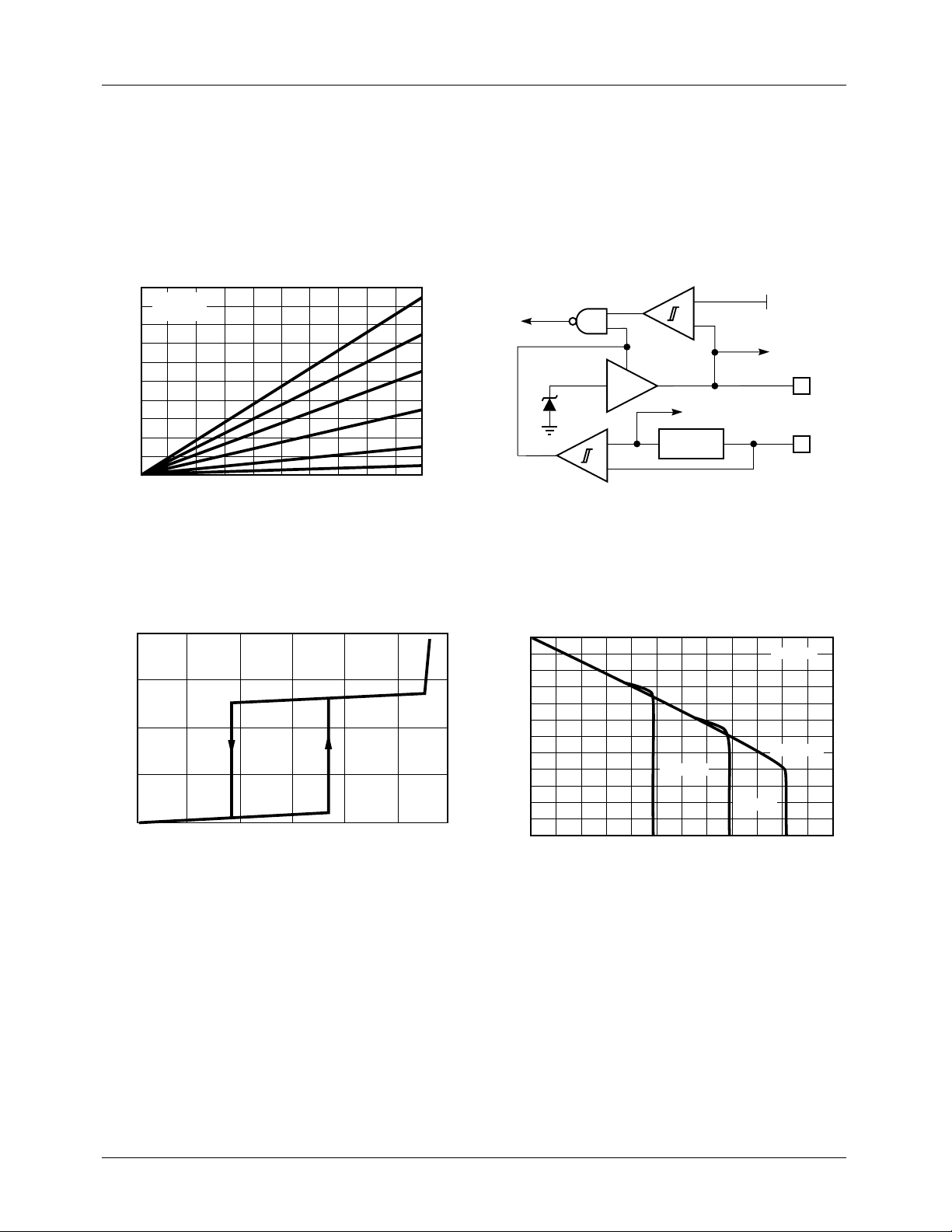
Under Voltage Lockout, OVP and Current Limit
On power-up the ML4821 remains in the UVLO condition;
output low and quiescent current low. The IC becomes
operational when VCC reaches 16V. When VCC drops below
9V, the UVLO condition is imposed. During the UVLO
condition, the V
for starting up a down-stream PWM converter.
500
RT = 5kΩ
V
RMS
400
300
200
100
MULTIPLIER OUTPUT CURRENT (µA)
0
0 100 300 400 500
Figure 7. Gain Modulator Linearity. Figure 8. Under-Voltage Lockout Block Diagram.
pin is “off”, making it usable as a “flag”
REF
= 3V
200
SINE INPUT CURRENT (µA)
5.5
E/A OUTPUT VOLTAGE
4.5
3.5
2.5
1.5
1.0
OVP, Shutdown, and IC Bias
When the input to the OVP comparator exceeds V
output of the ML4821 is inhibited. The OVP input also
functions as a “sleep” input, putting the IC into the low
quiescent UVLO state when the OVP pin is pulled below
0.7V.
–
+
ENABLE
V
REF
9V
–
+
INTERNAL
BIAS
4.4V
LOGIC
POWER
V
REF
V
CC
REF
, the
16
15
40
30
20
10
SUPPLY CURRENT (mA)
CC
I
0
0102030
V
SUPPLY VOLTAGE (V)
CC
Figure 9. Total Supply Current vs. Supply Voltage.
TA = 25°C
0
–4.0
–8.0
–12
–16
–20
, REFERENCE VOLTAGE CHANGE (mV)
REF
–24
∆V
0 20 40 60 80 100 120
, REFERENCE SOURCE CURRENT (mA)
I
REF
TA = 125°C
VCC = 15V
TA = –55°C
TA = 25°C
Figure 10. Reference Load Regulation.
8 REV. 1.0.2 6/19/01
Page 9
PRODUCT SPECIFICATION ML4821
Off-line Start-up and Bias Supply Generation
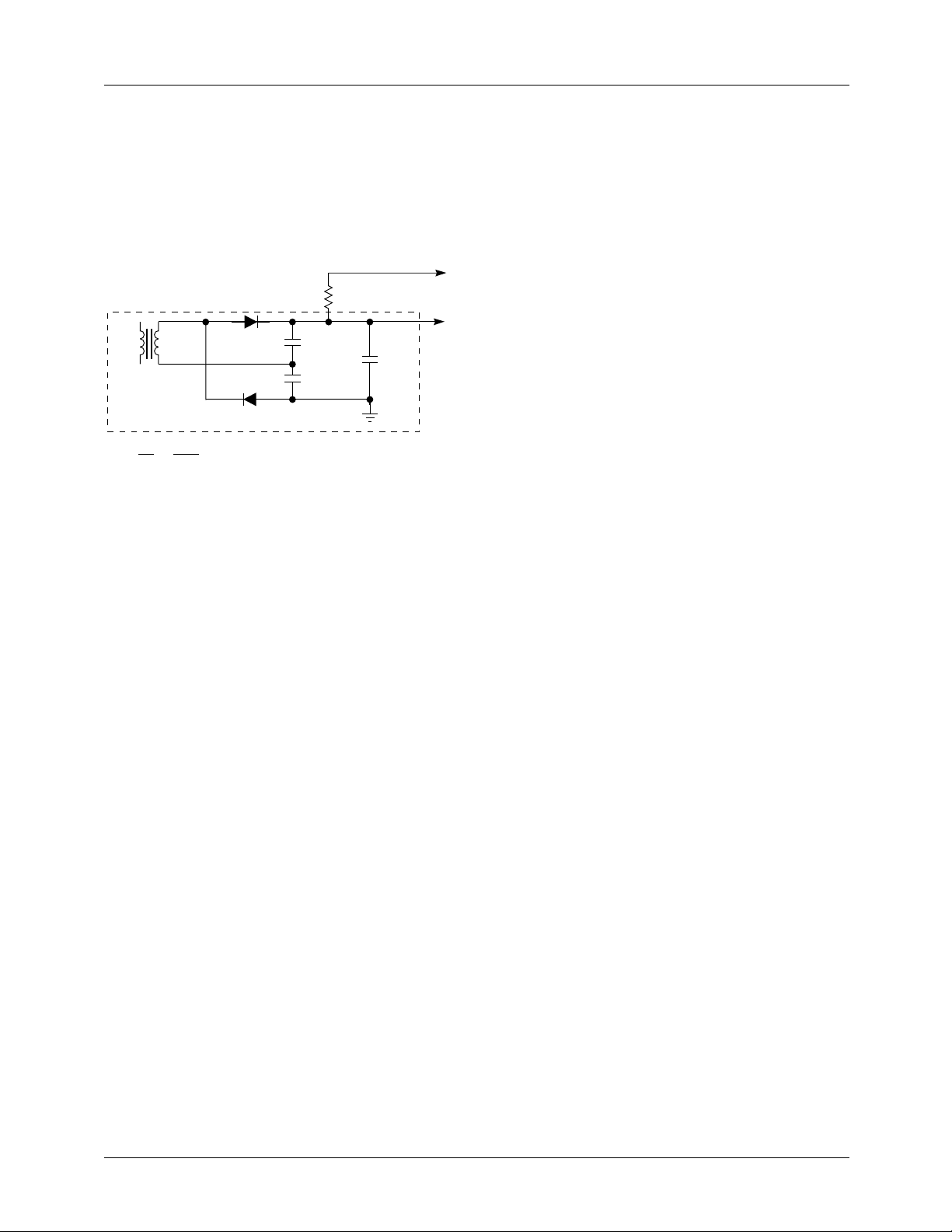
The circuit in Figure 11 supplies VCC power to the ML4821.
Start-up current is delivered via R10. The IC starts when
VCC reaches 15.5V. After that time running power is
delivered through the tap on L1. The configuration shown
delivers a voltage proportional to the PFC output bus
voltage.
R10
39kΩ
2W
L1
N
N
P
S
N
V
P
OUT
≈
N
14V
S
1µF
1µF
1000µF
TO B+
TO IC
PIN 15
Figure 11. Bias and Start-up Circuit.
REV. 1.0.2 6/19/01 9
Page 10
ML4821 PRODUCT SPECIFICATION
F1
AC IN
90-264
VAC
5A, 250V
C1
1µF
D1
D3
D2
D4
R10
39kΩ
R7
560kΩ
L1
D7
1N4934
D8
1N4934
C12
1µF
C13
1µF
R11
8.2kΩ
C14
470µF
D1
1N5406
D10
MUR850
C14
470µF
C19
270µF
450V
+
DC OUT
382V
–
R8
910kΩ
R9
91kΩ
R6
2.7kΩ
C2
120pF
R5
2kΩ
R13
20kΩ
C5
1.5nF
C3
0.1µF
91kΩ
R15
27kΩ
1N5406
1N5406
D5
D6
R1
0.25Ω
R12
2.7kΩ
C4
1.5nF
1
I
LIM
2
IA OUT
3
IA–
4
IA+
5
I
SINE
6
EA OUT
7
EA–
8
V
RMS
9
SOFT START
R14
C7
0.47µF
ML4821
C6
43nF
GND
C
V
REF
V
CC
OUT
PGND
R
OVP
SYNC
T
T
R21
6.2kΩ
18
17
16
15
14
13
12
11
10
R22
7.3Ω
C8
C10
0.1µF
R20
825kΩ
R19
10.2kΩ
C11
750pF
R18
825kΩ
R17
10.5kΩ
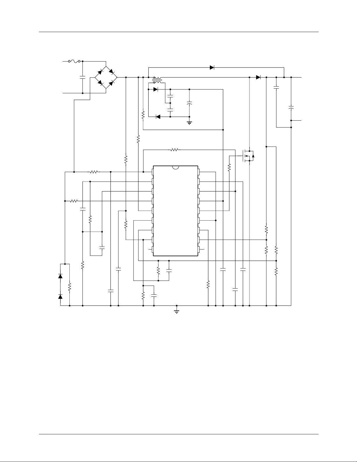
Figure 12. 200W Output PFC Circuit
10 REV. 1.0.2 6/19/01
Page 11
PRODUCT SPECIFICATION ML4821
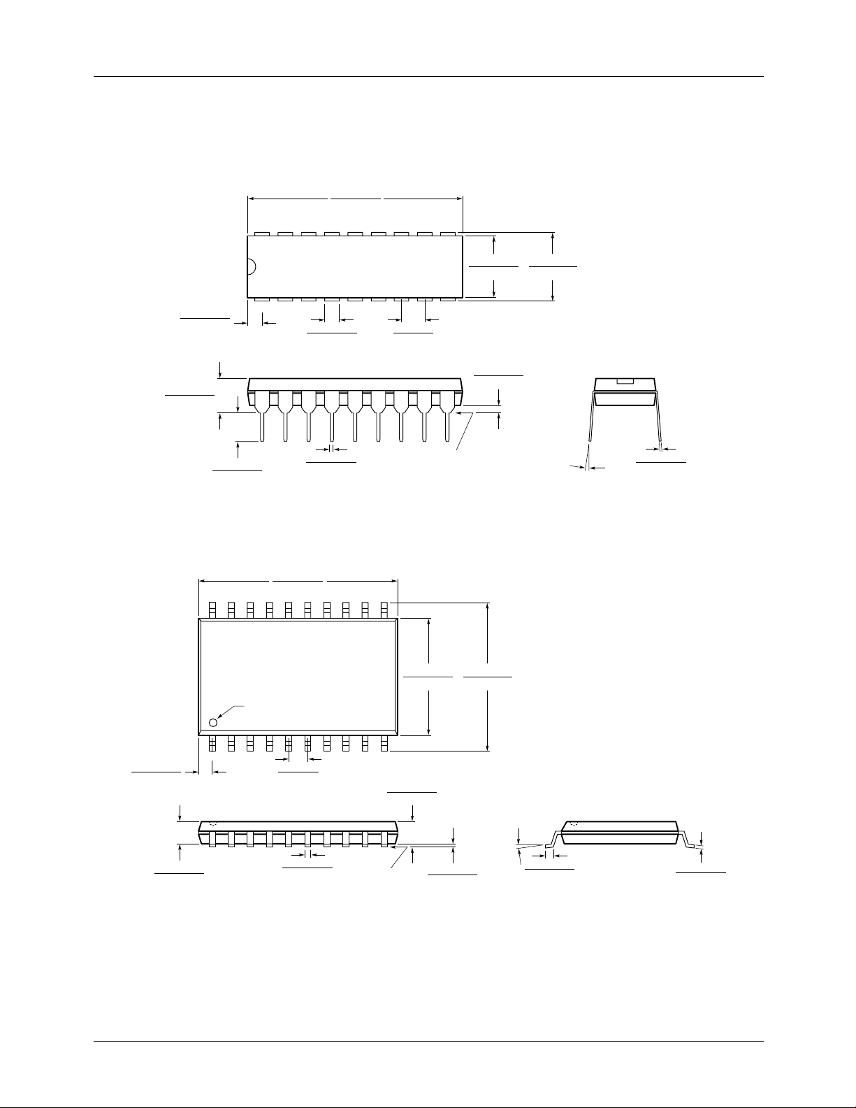
Mechanical Dimensions inches (millimeters)
Package: P18
18-Pin PDIP
0.890 - 0.910
(22.60 - 23.12)
18
0.045 MIN
(1.14 MIN)
(4 PLACES)
0.170 MAX
(4.32 MAX)
0.125 MIN
(3.18 MIN)
20
PIN 1 ID
1
0.498 - 0.512
(12.65 - 13.00)
0.050 - 0.065
(1.27 - 1.65)
0.016 - 0.022
(0.40 - 0.56)
0.100 BSC
(2.54 BSC)
SEATING PLANE
Package: S20
20-Pin SOIC
0.240 - 0.260
(6.09 - 6.61)
0.015 MIN
(0.38 MIN)
0.295 - 0.325
(7.49 - 8.26)
0º - 15º
0.008 - 0.012
(0.20 - 0.31)
0.024 - 0.034
(0.61 - 0.86)
(4 PLACES)
0.090 - 0.094
(2.28 - 2.39)
0.291 - 0.301
(7.39 - 7.65)
PIN 1 ID
1
0.050 BSC
(1.27 BSC)
0.012 - 0.020
(0.30 - 0.51)
0.095 - 0.107
(2.41 - 2.72)
SEATING PLANE
0.398 - 0.412
(10.11 - 10.47)
0.005 - 0.013
(0.13 - 0.33)
0º - 8º
0.022 - 0.042
(0.56 - 1.07)
0.007 - 0.015
(0.18 - 0.38)
REV. 1.0.2 6/19/01 11
Page 12

ML4821 PRODUCT SPECIFICATION
Ordering Information
Part Number Temperature Range Package
ML4821CP 0˚C to 70˚C 18-Pin PDIP (P18)
ML4821CS 0˚C to 70˚C 20-Pin SOIC (S20)
DISCLAIMER
FAIRCHILD SEMICONDUCTOR RESERVES THE RIGHT TO MAKE CHANGES WITHOUT FURTHER NOTICE TO
ANY PRODUCTS HEREIN TO IMPROVE RELIABILITY, FUNCTION OR DESIGN. FAIRCHILD DOES NOT ASSUME
ANY LIABILITY ARISING OUT OF THE APPLICATION OR USE OF ANY PRODUCT OR CIRCUIT DESCRIBED HEREIN;
NEITHER DOES IT CONVEY ANY LICENSE UNDER ITS PATENT RIGHTS, NOR THE RIGHTS OF OTHERS.
LIFE SUPPORT POLICY
FAIRCHILD’S PRODUCTS ARE NOT AUTHORIZED FOR USE AS CRITICAL COMPONENTS IN LIFE SUPPORT DEVICES
OR SYSTEMS WITHOUT THE EXPRESS WRITTEN APPROVAL OF THE PRESIDENT OF FAIRCHILD SEMICONDUCTOR
CORPORATION. As used herein:
1. Life support devices or systems are devices or systems
which, (a) are intended for surgical implant into the body,
or (b) support or sustain life, and (c) whose failure to
perform when properly used in accordance with
instructions for use provided in the labeling, can be
reasonably expected to result in a significant injury of the
user.
www.fairchildsemi.com
2. A critical component in any component of a life support
device or system whose failure to perform can be
reasonably expected to cause the failure of the life support
device or system, or to affect its safety or effectiveness.
6/19/01 0.0m 003
” 2001 Fairchild Semiconductor Corporation
Stock#DS30004821
 Loading...