

Page 1

April 1997
ML4813*
Flyback Power Factor Controller
GENERAL DESCRIPTION
The ML4813 is a PWM controller designed for use in a
discontinuous "flyback" or "buck-boost" type power factor
correction (PFC) system for low power, low cost
applications.
The circuit includes a precision reference, oscillator, error
amplifier, over-voltage comparator, over-current
comparator, and an extra op-amp as well as a high
current output. In addition, start-up is simplified by an
under-voltage lockout circuit.
In a typical application, the ML4813 functions as a
voltage mode regulator. By maintaining a constant duty
cycle, the current follows the input voltage, making the
impedance of the entire circuit appear purely resistive.
With the flyback circuit, power factors of 0.99 are easily
achievable with a small output inductor and a minimum
of external components.
BLOCK DIAGRAM
FEATURES
■ Precision buffered 5V reference
■ Extra op-amp for output voltage instrumentation
amplifier
■ Overcurrent comparator for switch protection
■ Soft start and under-voltage lockout for easy low surge
off-line starting
■ 1A peak current Totem-pole output drive
■ Overvoltage comparator eliminates output "runaway"
due to load removal
■ Large oscillator amplitude for better noise immunity
* This Part Is End Of Life As Of August 1, 2000
V
FB
4
SOFT START
2
I
LIMIT
1
OVP
5
COMP
3
C
T
16
R
T
9
SYNC
10
5V
1V
5.6V
ERROR
AMPLIFIER
+
CURRENT LIMIT
COMPARATOR
+
-
COMPARATOR
+
-
-
+
COMPARATOR
OSCILLATOR
OVP
PWM
7V
SRQ
Q
60µA
UNDERVOLTAGE
LOCKOUT
+
-
PWR GND
OA OUT
OA+
OA-
V
REF
V
CC
32V
OUT
GND
6
8
7
14
13
12
11
15
1
Page 2

ML4813
PIN CONFIGURATION
ML4813
16-Pin PDIP (P16)
16-Pin SOIC (S16W)
I
LIMIT
SOFT START
COMP
V
FB
OVP
OA OUT
OA-
OA+
PIN DESCRIPTION
PIN NAME FUNCTION
1I
LIMIT
2 SOFT START Connection for the soft start
3 COMP Output of error amplifier and input
4V
FB
5 OVP Overvoltage comparator input
Current limit sense pin which is
normally connected to the sense
resistor. When I
exceeds 1V,
LIMIT
the PWM cycle is terminated
capacitor
to the PWM comparator
Control loop feedback voltage
1
2
3
4
5
6
7
8
TOP VIEW
16
C
T
15
GND
14
V
REF
13
V
CC
12
OUT
11
PWR GND
10
SYNC
9
R
T
8 OA+ Non-inverting input of the
uncommitted op amp
PIN NAME FUNCTION
9R
T
Connection for the oscillator
timing resistor
10 SYNC Input for synchronizing the
oscillator to an external source
11 PWR GND Return for the high current output
transistors
12 OUT High current driver output
6 OA OUT Output of the uncommitted op
amp
7 OA- Inverting input of the uncommitted
op amp
2
13 V
14 V
CC
REF
Power supply input
Buffered reference output
15 GND Analog signal ground
16 C
T
Connection for the oscillator
timing capacitor
Page 3

ABSOLUTE MAXIMUM RATINGS
ML4813
Absolute maximum ratings are those values beyond
which the device could be permanently damaged.
Absolute maximum ratings are stress ratings only and
functional device operation is not implied.
Lead Temperature (Soldering, 10 sec) .....................260ºC
Thermal Resistance (qJA)
PDIP ................................................................ 88ºC/W
SOIC .............................................................. 105ºC/W
Supply Current .......................................................40mA
OUT Current .............................................................±1A
OUT Energy (capacitive load, per cycle) .................... 5µJ
OPERATING CONDITIONS
COMP Sink Current ............................................... 10mA
CT Charging Current................................................. 5mA
Analog Input Voltage (pins 1, 3-8) ....GND - 0.3V to 5.5V
Junction Temperature..............................................150ºC
Temperature Range
ML4813CX ................................................ 0ºC to 70ºC
ML4813IX ............................................... -40ºC to 85ºC
Storage Temperature Range ..................... –65ºC to 150ºC
ELECTRICAL CHARACTERISTICS
Unless otherwise specified, RT = 14kW, CT = 1nF, TA = Operating Temperature Range (Notes 1, 2)
PARAMETER CONDITIONS MIN TYP MAX UNITS
OSCILLATOR
Initial Accuracy Tj = 25ºC 90 97 104 kHz
Voltage Stability 12V < VCC < 18V 0.3 %
Temperature Stability 2%
Total Variation Line, temp 88 108 kHz
Ramp Valley 1.0 V
Ramp Peak 4.3 V
RT Voltage 4.8 5.0 5.2 V
Discharge Current Tj = 25ºC, V(CT) = 2V 7.5 8.4 9.3 mA
V(CT) = 2V 7.2 8.4 9.5 mA
SYNC Threshold 0.8 1.4 2.0 V
SYNC Bias Current 350 800 µA
REFERENCE
Output Voltage (V
Line Regulation 12V < VCC < 25V 6 20 mV
Load Regulation 1mA < I
Temperature Stability 0.4 %
Total Variation Line, load, temp 4.9 5.1 V
Output Noise 10Hz to 10kHz 50 µV
Long Term Stability Tj = 125ºC, 1000 hours 5 25 mV
Short Circuit Current V
)T
REF
< 20mA 3 20 mV
REF
= 25ºC, I
j
= GND -30 -85 -180 mA
REF
= 1mA 4.95 5.00 5.05 V
REF
3
Page 4
ML4813
ELECTRICAL CHARACTERISTICS (cont.)
PARAMETER CONDITIONS MIN TYP MAX UNITS
ERROR AMPLIFIER
Input Offset Voltage -15 15 mV
Input Bias Current -0.1 -1.0 µA
Open Loop Gain 1V < COMP < 5V 60 75 dB
PSRR 12V < VCC < 25V 60 70 dB
Output Sink Current COMP = 1.1V, VFB = 6.2V 2 12 mA
Output Source Current COMP = 5V, VFB = 4.8V -0.5 -1.0 mA
Output High Voltage I
Output Low Voltage I
Unity Gain Bandwidth 1.0 MHz
UNCOMMITTED OP AMP
Input Offset Voltage -10 10 mV
Input Bias Current -0.1 -2.0 µA
Input Offset Current -350 350 nA
Open Loop Gain 90 dB
PSRR 80 125 dB
Output High Voltage I
Output Low Voltage RL = 10kW 200 500 mV
I
COMPARATOR
LIMIT
Input Trip Point 0.8 1.0 1.2 V
Input Bias Current -2 -15 µA
Propogation Delay Time 150 ns
OVP COMPARATOR
Input Trip Point 5.4 5.55 5.7 V
= -10mA 6.5 8 V
COMP
= -0.5mA, VFB = 4.8V 5.3 6.4 V
COMP
= 2mA, VFB = 6.2V 0.5 1.0 V
COMP
Hysteresis 100 mV
Input Bias Current -0.3 3 181A
PWM COMPARATOR
Input Common Mode Range -0.2 5.5 V
Input Bias Current -2 -10 µA
Propogation Delay Time 150 ns
SOFT START
Soft Start Current V
SOFT START
= 1V 40 65 90 µA
4
Page 5

ML4813
ELECTRICAL CHARACTERISTICS (cont.)
PARAMETER CONDITIONS MIN TYP MAX UNITS
OUTPUT
Output Low Voltage I
I
= 200mA 1.2 2.2 V
OUT
VCC = 8V, I
Output High Voltage I
I
= -200mA 12 13.4 V
OUT
Rise/Fall Time CL = 1000pF 50 ns
UNDERVOLTAGE LOCKOUT
Start-up Threshold 15 16.3 17.5 V
Shutdown Threshold 9 10.1 11.2 V
V
Good Threshold 4.4 V
REF
SUPPLY
Start-up Current VCC = 14V 0.9 1.5 mA
Operating Current 20 30 mA
Shunt Regulator Voltage ICC = 30mA 25 30 34 V
Note 1: Limits are guaranteed by 100% testing, sampling, or correlation with worst-case test conditions.
Note 2: VCC is raised above the UVLO start-up threshold, then returned to 15V.
= 10mA 0.1 0.4 V
OUT
= 5mA 0.1 0.8 V
OUT
= -20mA 13 13.6 V
OUT
5
Page 6
ML4813
FUNCTIONAL DESCRIPTION
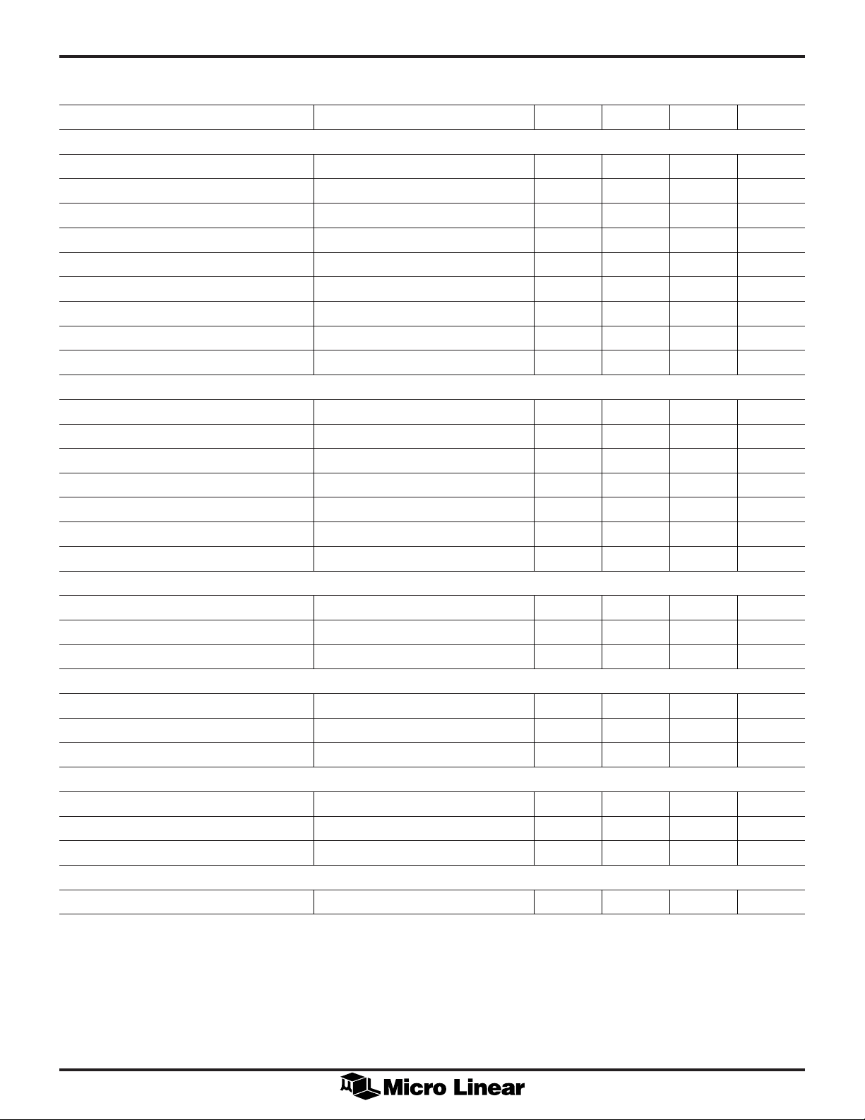
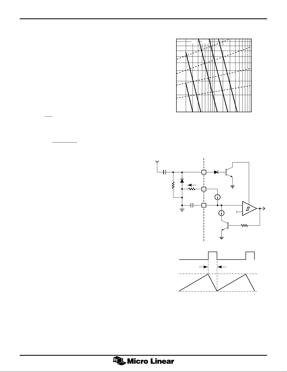
OSCILLATOR
The ML4813 oscillator charges the external capacitor (CT)
with a current (I
) equal to 5/R
SET
. When the capacitor
SET
voltage reaches the upper threshold, the comparator
changes state and the capacitor discharges to the lower
threshold through Q1. While the capacitor is discharging,
Q2 provides a high pulse.
The oscillator period can be described by:
tt t
=+
OSC RAMP DEADTIME
(1)
where:
C
t
RAMP
T
=
I
SET
(2)
and:
C
t
DEADTIME
=
T
mA I
-84.
SET
(3)
A graph showing the relationship between RT, CT, the
oscillator frequency, and maximum duty cycle is given in
Figure 1. A pulse of a duration shorter than t
DEADTIME
from an external frequency source set to a higher
frequency than f
synchronize the oscillator. R
can be applied to pin SYNC to
OSC
SYNC
and C
SYNC
shorten
longer pulses, as shown in Figure 2.
OUTPUT DRIVER STAGE
The ML4813 output driver is a 1A peak output high speed
totem-pole circuit designed to quickly drive capacitive
loads such as MOSFET gates. See Figure 3 for the output
saturation characteristics for sourcing and sinking current.
10
8
10nF
5
(kΩ)
T
R
3
20nF
2
1
10 100 1000
5nF 2nF
OSCILLATOR FREQUENCY (kHz)
90%
1nF
Figure 1. Oscillator Timing Resistance vs. Frequency
EXTERNAL
CLOCK
C
SYNC
R
SYNC
I
SET
R
C
SYNC
10
R
T
9
T
C
16
T
T
8.4mA
I
SET
5.6V
+
-
85%
MAXIMUM DUTY CYCLE (%)
80%
70%
ERROR AMPLIFIER
The ML4813 error amplifier is a high open loop gain,
wide bandwidth amplifier. See Figure 4 for the gain and
phase plot.
UN-COMMITTED OP-AMP
The ML4813 contains an uncommitted op amp which is
normally configured as a differencing amplifier to sense
the output voltage. The output voltage in the flyback
configuration is not ground referenced. The op amp in the
ML4813 is a PNP input amplifier similar to the LM324
but with an open emitter class A output stage.
REFERENCE
The reference output voltage versus output current
characteristic is shown in Figure 5.
UNDERVOLTAGE LOCKOUT
On power-up, the ML4813 is in the UVLO condition;
6
CLOCK
T
D
RAMP PEAK
V(CT)
RAMP VALLEY
Figure 2. Oscillator Block Diagram
output low and quiescent current low. The ML4813
becomes operational when VCC reaches 16V. When V
drops below 10V, the UVLO condition is re-imposed.
During UVLO, the V
pin is off, making it usable as a
REF
"flag" for starting up a down-stream PWM converter.
CC
Page 7

ML4813
15
V
CC
14
13
SOURCE SATURATION
LOAD TO GROUND
SINK SATURATION
LOAD TO V
3
2
1
OUTPUT SATURATION VOLTAGE (V)
0
0 200 400 800
CC
OUTPUT CURRENT (mA)
VCC = 15V
80µs PULSED LOAD
120Hz RATE
GND
600
Figure 3. Output Saturation Voltage vs. Output Current
0
-4
100
80
60
40
, Open Loop Gain (dB)
20
VOL
A
0
-20
25
20
100 10k 10M100k
10 1k 1M
Figure 4. Error Amplifier Open Loop
Gain and Phase vs. Frequency
Frequency (Hz)
GAIN
PHASE
0
-30
Excess Phase (degrees)
-60
-90
-120
-150
-180
-8
15
(mV)
-12
REF
∆V
-16
-20
-24
20 60 12080
0 40 100
I
(mA)
REF
(mA)
CC
I
10
5
0
0
VCC (V)
3020 4010
Figure 5. Reference Load Regulation vs. Output Current Figure 6. Supply Current vs. Supply Voltage
7
Page 8

ML4813
APPLICATIONS
The ML4813 is used to implement a discontinuous mode
flyback (buck-boost) power factor regulator as shown in
Figure 7. This topology is particularly well suited for low
power applications such as fluorescent ballasts and low
power switching supplies. It is also a useful topology
when there is a requirement for the output voltage to be
lower than the peak input voltage, or where an isolated
output is required. This is not possible with a boost
topology, where the output voltage must always be higher
than the maximum peak of the input voltage range. The
typical input range for the flyback power factor regulator
is from 90VAC to 260VAC.
The regulator operates in the discontinuous current
conduction mode. The inductor energy stored during the
ON time of the power switch Q is completely delivered
to the output capacitance during the OFF time. Under
steady state conditions, the inductor current at the
beginning of the ON time starts to ramp-up from 0 Amps
to a value that is determined by the instantaneous value
of the input full wave rectified voltage; the ON time as it
is set by the error amplifier and the PWM comparator;
and finally by the inductor itself.
The expression for the inductor peak current is given by:
Vt
q
05
q
=
IN ON
L
(4)
I
05
L
RFI
FILTER
C1
RH2
RL2
V
OUT-
V
OUT+
ML4813
CONTROLLER
RH1RL1
L1
–
V
S
+
D1
Q1
RS
Figure 7. Simplified Application Circuit
waveforms has not been preserved. Normally for 60Hz
input line and 100kHz switching frequency, each half of
the sine wave contains approximately 833 high frequency
triangular waveforms.
Where:
IL(q) = instantaneous peak inductor current
tON = Power MOSFET "ON" time
VIN(q) = VP sin q = Instantaneous input voltage
VP = Input peak voltage
Figure 8 shows the relationship between the low
frequency envelope and the high frequency inductor
current. Note that for clarity the scale between the two
The envelope of the peaks of the switch current, which in
this case represents the current drawn from the input
source, has a sinewave shape. This relationship is shown
as:
II
qq
=sin
0
5
LP
(5)
By combining (4) and (5), the following useful
relationship is obtained:
LI
t
=
ON
P
V
2
RMS
(6)
INDUCTOR CURRENT
SWITCH CURRENT
SINUSOIDAL PEAK ENVELOPE
AVERAGE CURRENT
Figure 8. Switch and Line Currents in the Flyback PFC Circuit
8
Page 9

APPLICATIONS (Continued)
ML4813
Note that VIN(q) = VP x sin(q) and that VP = 1.414 x V
The average value of the input triangular current is:
t
I
AVG
Where I
value of the current at the input of the regulator after
filtering), and T is the period of the switch cycle.
Substitution of (6) into (7) yields:
Equation (8) clearly shows that the average value of the
switch current is sinusoidal and in phase with the input
voltage. The peak value of the average current is:
Also:
Rearranging equations (9) and (10) to solve for P
For optimum performance and the lowest inductor peak
currents, the inductor current should be at the verge of
continuity at the lowest operating voltage point and at full
load. This can be satisfied if:
Finally, (11) and (12) can be combined to derive an upper
bound for the inductor value that will guarantee that the
regulator always stays in the discontinuous mode of
operation. If the regulator were to operate in the
continuous mode the average input current would not be
sinusoidal.
AVG
I
AVG
I
AVG PEAK
I
AVG PEAK
P
=
IN
I
P
L
!
FLYBACK INDUCTOR CALCULATION
Equation (13) gives the upper bound for the inductor
value for any set of specified operating conditions.
Normally, a few iterations may be required for finalizing
the value to correct for second or third order effects. This
means that a good initial value for the inductor is
probably 10 to 20% lower than the value calculated by
the right hand side expression in (13).
ON
qq
=
05
is the average value of the switch current (the
qq
=
05
()
()
LI f
VV
fL V V
+
2
fP V V
+
I
sin
P
T
2
2
LI
P
TV
2828.
LI
TV
.
2828
P
2
=
2
P
4
IN OUT
16
IN
V
RMS
IN OUT
VV
IN OUT
16
IN IN OUT
sin
RMS
2
P
RMS
2
"
#
#
$
sin=
q
yields:
IN
RMS
(7)
(8)
(9)
(10)
(11)
(12)
(13)
.
Several core materials are candidates for the inductor,
such as powder iron, gapped ferrites, moly permalloy, etc.
There are no particular restrictions on the inductor except
that the inductance is the correct value and the losses are
acceptable.
INPUT BYPASS CAPACITANCE
The triangular high frequency current is bypassed by an
input capacitor (CIN). This should be a high quality film
capacitor with low ESR value for minimum losses and
heating. Polyester, polypropylene or x-type (for line side)
are good candidates. Typical values, depending on the
power level, can range anywhere from 330nF to 1.5µF.
The next filtering stage of the RFI filter has an inductor as
an input to isolate CIN from the other capacitors which
may be present at the input circuit. Note that CIN can be
on either side of the bridge rectifier. The preferred
location for low crossover distortion is on the input side.
The ripple voltage across this capacitor is:
V
CP P
-
05
Where V
frequency capacitor voltage, and D is the switch duty
cycle. The RFI filter that follows CIN has to be able to
attenuate V
regulatory specifications.
INPUT TRANSIENT OVERVOLTAGE PROTECTION
Careful examination of the power circuits reveals that
there is no large capacitance at the input of the regulator.
The only capacitance present is that of the RFI filter
capacitors. These capacitors have a combined value in the
range of a few microfarads, and their ability to absorb and
minimize any line induced transients is almost
nonexistent. Transients can also occur under sudden load
removal. If the line impedance is inductive, hazardous
drain-source voltages may be generated leading to the
destruction of the power MOSFET. To keep this from
happening, a transient over-voltage protection device
should be installed such that enough safety margin is
allowed for the power MOSFET. A good rule of thumb is:
Where BV
the MOSFET, V
of the over-voltage transient protector, and V
the maximum output voltage which is set by the OVP
function of the controller.
THE OUTPUT CIRCUIT
The output circuit for this topology, although nonisolated, does not share the same ground with the power
circuit. Therefore connecting the two grounds with the
measuring leads of instruments should be avoided.
C(P-P)
BV V V
DSS CLAMP OUT OVP
D
=
Cf
is the peak to peak worst case high
C(P-P)
>+
is the drain-source breakdown voltage for
DSS
CLAMP
IN
to the levels set by the relevant
is the activation or clamping voltage
P
IN IN
-
LfPCfV
()
2
IN IN
OUT(OVP)
(14)
(15)
is
9
Page 10

ML4813
OUT
V
10nF
R1
330µF
1kV
220kΩ
250V
-
CIRCUIT
START-UP
1%
R13
402kΩ
D6
MUR460
Q2
IRF821
R14
402kΩ
L3
1%
R23
C5
1kV
10nF
D5
1N4148
D9
22V
D8
1N4148
C14
100nF
Q3
2N2222
R22
2kΩ
2kΩ
C10
C11
6.8nF
100nF
C8
C9
D7
MUR460
R2
4.3kΩ
1000µF
1µF
Q1
MTH8N60
CIRCUIT
ENHANCEMENT
R3
10Ω
C7
R10
1nF
R9
1Ω
R8
1Ω
R7
1Ω
R6
1Ω
R5
1Ω
100Ω
R4
1Ω
+
C3
C4
L1
F1
C2
500µH
C1
3A
680nF
680nF
VR1
630V
630V
275V
L2
500µH
R13
SYNC
R11
1.8kΩ
T
C
GND
REF
V
V
CC
OUT
SYNC
T
R
PWR GND
ML4813
LIMIT
I
SOFT START
COMP
VFBOVP
OA OUT
OA-
OA+
1%
R12
4.02kΩ
1%
R17
R25
806kΩ
3.83kΩ
R24
C13
1%
402kΩ
R14
1%
R13
C12
402kΩ
402kΩ
220nF
4.7µF
1%
100kΩ
R14
1%
402kΩ
1%
R18
200Ω
10
LINE
INPUT
Figure 9. 80W Flyback Power Factor Regulator Using the ML4813
Page 11

APPLICATIONS (Continued)
The output voltage "rides" on the input voltage when the
(+) output is measured with respect to PWR GND as
shown in Figure 10.
ML4813
The extra op amp provided in the ML4813 can be used to
sense the output voltage for regulation and overvoltage
conditions. This op amp is connected as a difference
amplifier with its output referenced to PWR GND.
Resistors RH1, RH2, RL1, RL2 are used to scale down the
voltage.
Normally, RH1 = RH2 = RH and RL1 = RL2 = RL. The
voltage designated as VS in Figure 7 is given by:
VV
=
SOUT
RL
RH RL
+
(16)
The output capacitance should be calculated such that it
has the required output ripple at the worst case operating
point. In addition, the ESR should be sufficiently low to
prevent excessive dissipation due to RMS currents. The
first criterion can be met by choosing the value of the
output capacitor based on the following:
P
C
OUT
IN
fVV
2pD
LROUT
(17)
Where:
C
= Total output capacitance
OUT
PIN = Total input power
DVR = Peak output capacitor ripple voltage
fL = Line frequency times 2 (120 for 60Hz line)
The second criterion for the selection of the output
capacitor can be satisfied by choosing a component with
adequately low ESR value that can safely bypass the RMS
currents.
OUTPUT DIODE
The output diode can be a "fast" or ultrafast' type
depending on the operating frequency. Reverse recovery
losses are low since under normal operating conditions,
the regulator operates in discontinuous current mode. The
diode should be rated to handle the maximum output
current. The resulting power dissipation will be the
forward drop of the diode times the output current.
POWER SWITCH
If a power MOSFET is used, it should be sized for the
required efficiency. Lower R
devices will yield
DS(ON)
lower losses, but if they are operated at high frequencies
(100kHz), higher charge dumping losses will be
experienced. The RMS current value through the power
FET and the sensing resistor is:
I
RMS
LI f
=
424.
3
PL
V
RMS
Ê
k
r
=
1
sin
k
2
p
r
(15)
200V
V
OUT
V
OUT+
VOLTAGE
V
PWR GND
OUT-
TIME
Figure 10. Output Voltage with Respect to PWR GND
Where:
I
= Total RMS current through the power MOSFET
RMS
fL = Line frequency times 2 (120 for 60Hz line)
r = f
SWITCH/fL
Table 1 is provided to assist in calculating (18). When the
power switch is a bipolar transistor (constant VCE drop),
then the power dissipation produced can be calculated
by:
P
09.
P
=
D
IN
V
V
RMS
CE
(19)
Where:
PD = Power dissipation in the transistor
V
= RMS value of the minimum input voltage
RMS
VCE = Forward drop of the power transistor
r
k
p
f
SWITCH
(kHz) r
Ê
k
2
sin
=
r
1
20 167 9.1
30 250 11.2
40 333 12.9
50 417 14.4
60 500 25.8
70 583 17.1
80 667 18.3
90 750 19.4
100 833 20.4
110 917 21.4
120 1000 22.4
130 1083 23.3
140 1167 24.2
150 1250 25.0
160 1333 25.7
170 1417 26.5
180 1500 27.3
190 1583 28.0
200 1667 28.9
Table 1. Constants for Calculating IRMS (Equation 18)
11
Page 12

ML4813
APPLICATIONS (Continued)
OFF-LINE START-UP AND BIAS SUPPLY GENERATION
A fast starting circuit is included in Figure 9. MOSFET Q2
quickly charges the ML4813 VCC capacitor (C8) when the
supply is initially turned on. This allows the supply to
come on less than 1 second after AC power is applied. A
simpler start-up circuit may be used which replaces the
active circuit with a 39kW, 2W resistor but starts more
slowly (up to 15 seconds under low line conditions).
Systems which do not require quick starting can reduce
cost with the latter start-up method.
POWER FACTOR ENHANCEMENT
Some combinations of line and load may exhibit
distortion of the input current waveform. This distortion is
usually caused by the inductor "ringing" with the CDS of
the power MOSFET, resulting in a non-zero inductor
current at the beginning of the next cycle. This ringing
can be dampened by using R2 and D7 as shown in Figure
9. Applications which can get by with slightly worse
power factor can eliminate these components.
ADJUSTING THE OUTPUT VOLTAGE
The error amplifier creates an error voltage from the
difference between the output voltage presented at OA
OUT and the 5V internal reference. Since the output
voltage is not ground referenced, the ML4813's internal
op amp is connected as an instrumentation amplifier as
shown in Figure 11.
R12
V
OUT+
V
OUT-
Figure 11. Ground Referencing the Op Amp Output
R14'
R15'
Figure 12. Setting OVP at > 1.12 x V
OA+
OA-
OA OUT
+
–
R25
OVP
ML4813
RARB
OA OUT
ERROR AMP
R17
R18
OUT
TO
AND OVP
The output voltage is set by resistors which determine the
relationship between (V
the op amp. For the following discussion, R15' = R15 +
R16 and R14' = R13 + R14. The differencing amplifier
depends on the following relationships:
R14'= R15'
R12 = R25 + (R17 || R18)
Then:
VR
+
518
V
Since R25 is a low value compared to R15', the second
term reduces to approximately 1. The third term is set at
approximately 200. Equation (20) can be reduced to:
V
The overvoltage comparator has a threshold that is set for
1.12 x V
directly. Figure 12 shows the connection for setting an
OVP trip point higher than 1.12 x V
VV
=
OUT
RR
+
17 18
@
1000
OUT
when OVP and OA OUT are connected
OUT
@
112.
OVP OUT
RR
- V
OUT+
RR25
R
18
+
17 18
RR
AB
) and the output of
OUT-
R
15
’
+
+
15
’
OUT
+
R
B
R
14
’
R
, where:
1
12
(20)
(21)
(22)
+
RD
COMP
V
FB
ML4813
OVP
OA OUT
OUT
(23)
C13
R24RD
Figure 13. Setting OVP at < 1.12 x V
Figure 15 shows OVP set for a voltage lower than 1.12 x
V
where:
OUT
RD R24
VV
@
112.
OVP OUT
12
Page 13

APPLICATIONS (Continued)
INDUCTOR INFORMATION
L3 is the flyback inductor and also provides the operating
power for the control circuitry. A gapped ferrite pot core
was chosen for this application for it's modest high
frequency losses with high ripple current operation. Some
possible choices are:
ML4813
SHORTED TURN
(COPPER FOIL)
Manufadurer Part # Total Gap N
Magnetics Inc. F43019 0.05" 32
Phillips 3019 PL00-3F3 0.05" 32
Phillips 3019 PA125-3C8 0.07" 38
The first 2 cores are sold ungapped and require the use of
a .025. spacer to gap the center leg to yield a total gap
length of 0.05". If an ungapped core is used, a "shorted
turn" should be employed as shown in Figure 14 to
prevent radiated EMI. The third core listed is sold with its
center ieg pre-gapped (0.07" total) so that the outside of
the core closes completely, providing shielding without a
shorted turn. NS should be 3 turns. All windings are
#24AWG wire.
Inductors L1 and L2 are constructed using a powdered
iron. This is a suitable material for these inductors since
the high frequency ripple currents (and resulting flux
excursions) are much less severe than for L3. The core
selected is a MicroMetals T68-26D with 80 turns or
#24AWG wire.
P
0.25" SPACER
Figure 14. EMI Shielding for Ungapped Cores
WINDINGS
13
Page 14

ML4813
PHYSICAL DIMENSIONS inches (millimeters)
Package: P16
16-Pin PDIP
0.740 - 0.760
(18.79 - 19.31)
16
0.02 MIN
(0.50 MIN)
(4 PLACES)
0.170 MAX
(4.32 MAX)
0.125 MIN
(3.18 MIN)
16
PIN 1 ID
1
0.055 - 0.065
(1.40 - 1.65)
0.016 - 0.022
(0.40 - 0.56)
0.400 - 0.414
(10.16 - 10.52)
0.240 - 0.260
(6.09 - 6.61)
0.100 BSC
(2.54 BSC)
0.015 MIN
(0.38 MIN)
SEATING PLANE
Package: S16W
16-Pin Wide SOIC
0.295 - 0.325
(7.49 - 8.26)
0º - 15º
0.008 - 0.012
(0.20 - 0.31)
14
0.024 - 0.034
(0.61 - 0.86)
(4 PLACES)
0.090 - 0.094
(2.28 - 2.39)
1
PIN 1 ID
0.050 BSC
(1.27 BSC)
0.012 - 0.020
(0.30 - 0.51)
0.291 - 0.301
0.095 - 0.107
(2.41 - 2.72)
SEATING PLANE
(7.39 - 7.65)
0.005 - 0.013
(0.13 - 0.33)
0.398 - 0.412
(10.11 - 10.47)
0º - 8º
0.022 - 0.042
(0.56 - 1.07)
0.009 - 0.013
(0.22 - 0.33)
Page 15

ML4813
ORDERING INFORMATION
PART NUMBER TEMPERATURE RANGE PACKAGE
ML4813CP (EOL) 0°C to 70°C 16-Pin PDIP (P16)
ML4813CS (Obsolete) 0°C to 70°C 16-Pin SOIC (S16W)
ML4813IP (Obsolete) -40°C to 85°C 16-Pin PDIP (P16)
ML4813IS (Obsolete) -40°C to 85°C 16-Pin SOIC (S16W)
© Micro Linear 1996 is a registered trademark of Micro Linear Corporation.
Products described herein may be covered by one or more of the following U.S. patents: 4,897,611; 4,964,026; 5,027,116; 5,281,862; 5,283,483; 5,418,502; 5,508,570;
5,510,727; 5,523,940; 5,546,017; 5,559,470; 5,565761; 5,592,128; 5,594,376. Japan: 2,598,946; 2,619,299. Other patents are pending.
Micro Linear reserves the right to make changes to any product herein to improve reliability, function or design. Micro Linear does not assume any liability arising out of
the application or use of any product described herein, neither does it convey any license under its patent right nor the rights of others. The circuits contained in this data
sheet are offered as possible applications only. Micro Linear makes no warranties or representations as to whether the illustrated circuits infringe any intellectual property
rights of others, and will accept no responsibility or liability for use of any application herein. The customer is urged to consult with appropriate legal counsel before
deciding on a particular application.
DS4813-01
2092 Concourse Drive
San Jose, CA 95131
Tel: 408/433-5200
Fax: 408/432-0295
15
 Loading...