

Page 1
www.fairchildsemi.com
ML4812
Power Factor Controller
Features
• Precision buffered 5V reference (±0.5%)
• Current-input gain modulator reduces external
components and improves noise immunity
• Programmable ramp compensation circuit
• 1A peak current totem-pole output drive
• Overvoltage comparator helps prevent output voltage
“runaway”
• Wide common mode range in current sense comparators
for better noise immunity
• Large oscillator amplitude for better noise immunity
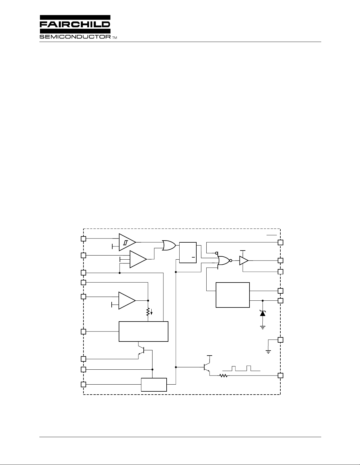
Block Diagram
(Pin Configuration Shown is for DIP Version)
OVP
5
I
SENSE
1
GM OUT
2
EA OUT
3
EA–
4
5V
5V
5V
+
–
+
–
+
–
–
ERROR
AMP
I
EA
Description
The ML4812 is designed to optimally facilitate a peak
current control boost type power factor correction system.
Special care has been taken in the design of the ML4812 to
increase system noise immunity. The circuit includes a
precision reference, gain modulator, error amplifier, overvoltage protection, ramp compensation, as well as a high
current output. In addition, start-up is simplified by an undervoltage lockout circuit with 6V hysteresis.
In a typical application, the ML4812 functions as a current
mode regulator . The current which is necessary to terminate
the cycle is a product of the sinusoidal line voltage times the
output of the error amplifier which is regulating the output
DC voltage. Ramp compensation is programmable with an
external resistor, to provide stable operation when the duty
cycle exceeds 50%.
SHDN
V
32V
OUT
REF
V
CC
10
12
11
14
13
SRQ
V
CC
Q
PWR GND
UNDER
VOLTAGE
LOCKOUT
I
SINE
6
RAMP COMP
7
C
T
16
R
T
8
GAIN MODULATOR
OSC
5V
1kΩ
GND
15
CLOCK
9
REV. 1.0.4 5/31/01
Page 2
ML4812 PRODUCT SPECIFICATION
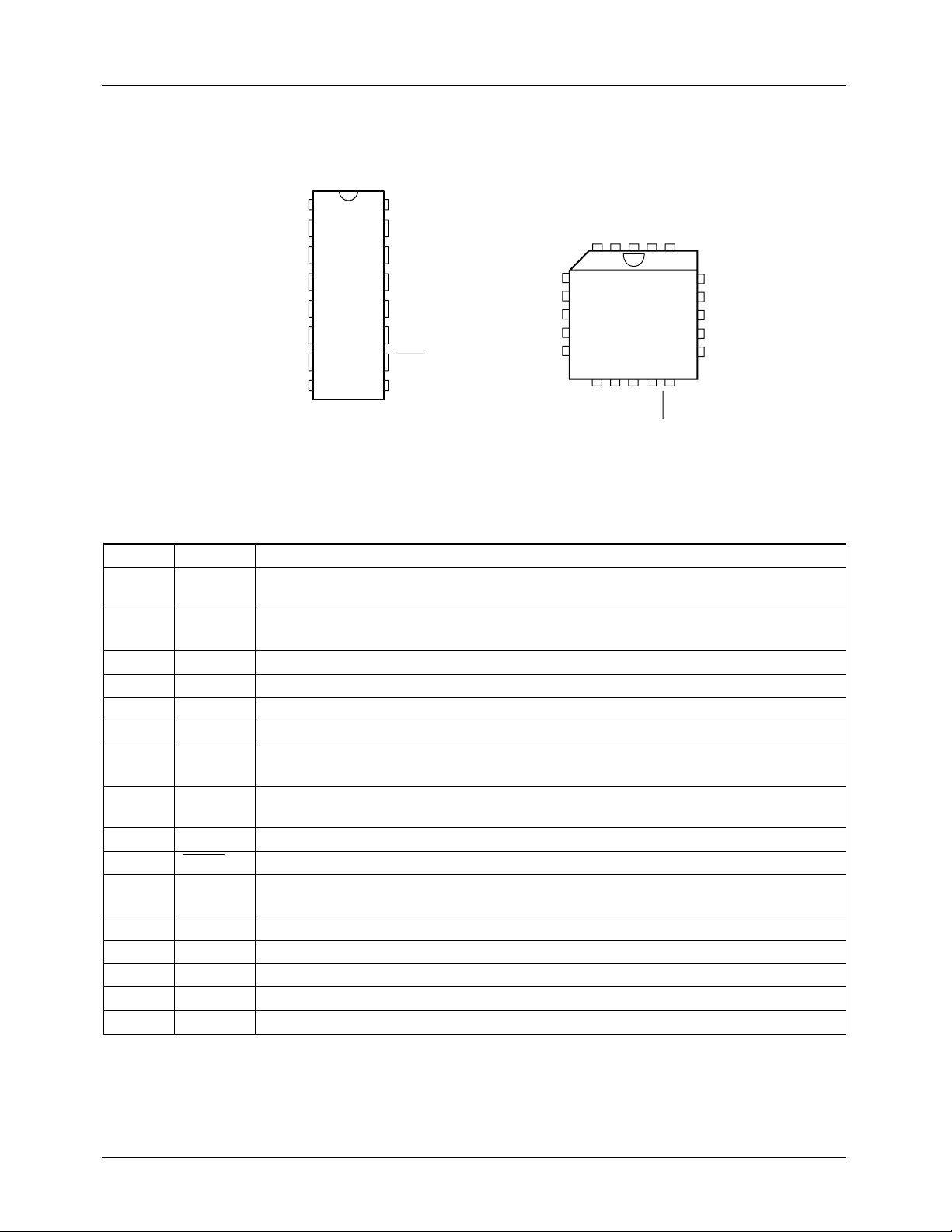
Pin Configuration
ML4812
20-Pin PLCC (Q20)
SENSE
GM OUT
I
NC
CTGND
3212019
NC
SHDN
CLOCK
18
17
16
15
14
4
5
6
7
8
910111213
T
R
RAMP COMP
Top View
V
REF
V
CC
NC
OUT
PWR GND
16-Pin PDIP (P16)
I
SENSE
GM OUT
EA OUT
EA–
OVP
I
SINE
RAMP COMP
R
T
ML4812
1
2
3
4
5
6
7
8
Top View
16
15
14
13
12
11
10
9
C
T
GND
V
REF
V
CC
OUT
PWR GND
SHDN
CLOCK
EA OUT
EA–
NC
OVP
I
SINE
Pin Description
Number Name Function
1 I
SENSE
2 GM OUT Output of gain modulator. A resistor to ground on this pin converts the current to a
3 EA OUT Output of error amplifier.
4EA– Inverting input to error amplifier.
5 OVP Input to over voltage comparator.
6 I
SINE
7 RAMP
COMP
8R
T
9 CLOCK Digital clock output.
10 SHDN A TTL compatible low level on this pin turns off the output.
11 PWR
GND
12 OUT High current totem pole output.
13 V
14 V
CC
REF
15 GND Analog signal ground.
16 C
T
Input from the current sense transformer to the non-inverting input of the PWM
comparator.
voltage. This pin is clamped to 5V and tied to the inverting input of the PWM comparator.
Current gain modulator input.
Buffered output from the oscillator ramp (C
is internally subtracted from the product of I
). A resistor to ground sets the current which
T
SINE
and I
in the gain modulator.
EA
Oscillator timing resistor pin. A 5V source sets a current in the external resistor which is
mirrored to charge C
.
T
Return for the high current totem pole output.
Positive Supply for the IC.
Buffered output for the 5V voltage reference.
Timing capacitor for the oscillator.
2
REV. 1.0.4 5/31/01
Page 3

ML4812 PRODUCT SPECIFICATION
Absolute Maximum Ratings
Supply Current (I
) 30mA
CC
1
Output Current Source or Sink (OUT) DC 1.0A
Output Energy (capacitive load per cycle) 5µJ
Gain Modulator I
SINE
Input (I
) 1.2mA
SINE
Error Amp Sink Current (EA OUT) 10mA
Oscillator Charge Current 2mA
Analog Inputs (I
, EA–, OVP) –0.3V to 5.5V
SENSE
Junction Temperature 150°C
Storage Temperature Range –65°C to 150°C
Lead Temperature (soldering 10 sec.) 260°C
Thermal Resistance ( θ
20-Pin PLCC
16-Pin PDIP
Note:
1. Absolute maximum ratings are those values beyond which the device could be permanently damaged. Absolute maximum
ratings are stress ratings only and functional device operation is not implied.
JA
)
60°C/W
65°C/W
Operating Conditions
Temperature Range
ML4812CX 0°C to 70°C
3
REV. 1.0.4 5/31/01
Page 4
PRODUCT SPECIFICATION ML4812
Electrical Characteristics
Unless otherwise specified, V
Parameter Conditions Min. Typ. Max. Units
Oscillator
Initial Accuracy T
Voltage Stability 12V < V
Temperature Stability 2 %
Total Variation Line, temperature 90 108 kHz
Ramp Valley to Peak 3.3 V
R
Voltage 4.8 5.0 5.2 V
T
Discharge Current (R
open) T
T
Clock Out Voltage Low RL = 16k Ω
Clock Out Voltage High RL = 16k Ω
Reference
Output Voltage T
Line Regulation 12V < V
Load Regulation 1mA < IO < 20mA 2 20 mV
Temperature Stability 0.4 %
Total Variation Line, load, temp. 4.9 5.1 V
Output Noise Voltage 10Hz to 10kHz 50 µV
Long Term Stability T
Short Circuit Current V
Error Amplifier
Input Offset Voltage ±15 mV
Input Bias Current –0.1 –1.0 µA
Open Loop Gain 1 < V
PSRR 12V < V
Output Sink Current V
Output Source Current V
Output High Voltage I
Output Low Voltage I
Unity Gain Bandwidth 1.0 MHz
Gain Modulator
I
Input Voltage I
SINE
Output Current (GM OUT) I
Bandwidth 200 kHz
PSRR 12V < V
= 15V , R
CC
= 14k Ω , C
T
= 25°C 91 98 105 kHz
J
< 18V 0.3 %
CC
= 25°C, V
J
V
= 2V 7.3 8.4 9.3 mA
CT
= 1000pF, T
T
= 2V 7.8 8.4 9.0 mA
CT
= Operating Temperature Range (Notes 1, 2).
A
0.2 0.5 V
3.0 3.5 V
= 25°C, I
J
= 125°C, 1000 hours 5 25 mV
J
= 0V –30 –85 –180 mA
REF
EA OUT
EA OUT
EA OUT
EA OUT
EA OUT
= 500µA 0.4 0.7 0.9 V
SINE
= 500µA, EA– = V
SINE
I
= 500µA, EA– = V
SINE
I
= 1mA, EA– = V
SINE
I
= 500µA, EA– = V
SINE
I
RAMP COMP
= 1mA 4.95 5.00 5.05 V
O
< 25V 2 20 mV
CC
< 5V 60 75 dB
< 25V 60 75 dB
CC
= 1.1V, V
= 5.0V, V
= –0.5mA, V
= 1mA, V
= 6.2V 2 12 mA
EA–
– = 4.8V –0.5 –1.0 mA
EA
– = 4.8V 5.3 5.5 V
EA
– = 6.2V 0.5 1.0 V
EA
– 20mV 430 470 510 µA
REF
+ 20mV 3 10 µA
REF
– 20mV 860 940 1020 µA
REF
REF
– 20mV,
455 µA
= 50µA
< 25V 70 dB
CC
REV. 1.0.4 5/31/01
4
Page 5
ML4812 PRODUCT SPECIFICATION
Electrical Characteristics
Unless otherwise specified, V
CC
(Continued)
= 15V , R
= 14k Ω , C
T
= 1000pF, T
T
= Operating Temperature Range (Notes 1, 2).
A
Parameter Conditions Min. Typ. Max. Units
OVP Comparator
Input Offset Voltage Output Off –25 +5 mV
Hysteresis Output On 95 105 115 mV
Input Bias Current –0.3 –3µA
Propagation Delay 150 ns
PWM Comparator: I
SENSE
Input Offset Voltage ±15 mV
Input Offset Current ±1 µA
Input Common Mode Range –0.2 5.5 V
Input Bias Current –2 –10 µA
Propagation Delay 150 ns
I
Trip Point V
LIMIT
GM OUT
= 5.5V 4.8 5 5.2 V
Output
Output Voltage Low I
Output Voltage High I
Output Voltage Low in UVLO I
Output Rise/Fall Time C
Shutdown V
= –20mA 0.1 0.4 V
OUT
I
= –200mA 1.6 2.2 V
OUT
= 20mA 13 13.5 V
OUT
I
= 200mA 12 13.4 V
OUT
= –5mA, V
OUT
= 1000pF 50 ns
L
IH
V
IL
I
, V
IL
IIH, V
= 0V –1.5 mA
SHDN
= 5V 10 µA
SHDN
= 8V 0.1 0.8 V
CC
2.0 V
0.8 V
Under-Voltage Lockout
Startup Threshold 15 16 17 V
Shutdown Threshold 9 10 11 V
V
Good Threshold 4.4 V
REF
Supply
Supply Current Start-Up, V
Operating, T
Internal Shunt Zener Voltage I
Notes:
1. Limits are guaranteed by 100% testing, sampling, or correlation with worst-case test conditions.
2. V
is raised above the Startup Threshold first to activate the IC, then returned to 15V.
CC
= 30mA 25 30 34 V
CC
= 14V, T
CC
= 25°C2025mA
J
= 25°C 0.8 1.2 mA
J
5
REV. 1.0.4 5/31/01
Page 6
ML4812 PRODUCT SPECIFICATION
Functional Description
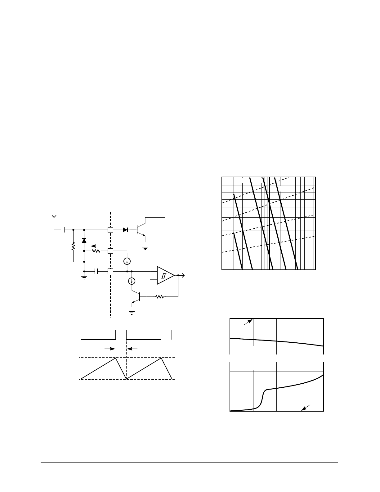
Oscillator
The ML4812 oscillator charges the external capacitor (CT)
with a current (I
voltage reaches the upper threshold, the comparator changes
state and the capacitor discharges to the lower threshold
through Q1. While the capacitor is discharging, Q2 provides
a high pulse.
EXTERNAL
CLOCK
C
SYNC
R
SYNC
) equal to 5/R
SET
I
SET
R
T
C
T
10
9
16
. When the capacitor
SET
SYNC
R
T
I
T
8.4mA
SET
5.6V
C
Q
2
+
-
The Oscillator period can be described by the following
relationship:
T
OSCTRAMPTDEADTIME
+=
where:
OUT
--------------------=
1D
–
ON
V
V
IN
and:
CTV
×
T
DEADTIME
10
8
5
(kΩ)
T
R
3
2
1
10 100 1000
5nF 2nF
10nF
20nF
OSCILLATOR FREQUENCY (kHz)
RAMPVALLEYTOPEAK
-------------------------------------------------------------------------=
8.4mA I
1nF
–
SET
90%
85%
80%
70%
MAXIMUM DUTY CYCLE (%)
RAMP PEAK
RAMP VALLEY
6
Q
1
CLOCK
t
D
V(CT)
Figure 1. Oscillator Block Diagram
Figure 2. Oscillator Timing Resistance vs. Frequency
15
V
CC
14
13
SOURCE SATURATION
LOAD TO GROUND
SINK SATURATION
LOAD TO V
3
2
1
OUTPUT SATURATION VOLTAGE (V)
0
0 200 400 800
CC
OUTPUT CURRENT (mA)
VCC = 15V
80µs PULSED LOAD
120Hz RATE
GND
600
Figure 3. Output Saturation Voltage vs. Output Current
REV. 1.0.4 5/31/01
Page 7

PRODUCT SPECIFICATION ML4812
Output Driver Stage
The ML4812 output driver is a 1A peak output high speed
totem pole circuit designed to quickly dri v e capacitive loads,
such as power MOSFET gates. (Figure 3)
Error Amplifier
The ML4812 error amplifier is a high open loop gain, wide
bandwidth, amplifier.(Figures 4-5)
Gain Modulator
The ML4812 gain modulator is of the current-input type to
provide high immunity to the disturbances caused by high
power switching. The rectified line input sine wave is converted to a current via a dropping resistor. In this way , small
amounts of ground noise produce an insignificant effect on
the reference to the PWM comparator. The output of the gain
modulator is a current of the form: I
I
↔ IEA, where I
SINE
is the current in the dropping
SINE
resistor, and IEA is a current proportional to the output of the
5V
+
is proportional to
OUT
8V
0.5mA
error amplifier. When the error amplifier is saturated high,
the output of the gain modulator is approximately equal to
the I
input current. The gain modulator output current is
SINE
converted into the reference voltage for the PWM comparator through a resistor to ground on the gain modulator output. The gain modulator output is clamped to 5V to provide
current limiting.
Ramp compensation is accomplished by subtracting 1/2 of
the current flowing out of RAMP COMP through a buffer
transistor driven by C
which is set by an external resistor .
T
Under V oltage Lockout
On power-up the ML4812 remains in the UVLO condition;
output low and quiescent current low. The IC becomes operational when VCC reaches 16V. When VCC drops below
10V, the UVLO condition is imposed. During the UVLO
condition, the 5V VREF pin is “off”, making it usable as a
“flag” for starting up a downstream PWM converter.
ERROR CURRENT
I
SINE
6
9V
I
– I
ERROR CURRENT
SINE ×
RAMP COMP
/2
EA–
4
EA OUT
3
–
Figure 4. Error Amplifier Configuration
100
80
60
40
20
, OPEN LOOP GAIN (dB)
VOL
A
0
-20
100 10k 10M100k
10 1k 1M
GAIN
FREQUENCY (Hz)
PHASE
0
-30
EXCESS PHASE (degrees)
-60
-90
-120
-150
-180
GM OUT
2
RAMP COMP
7
C
T
16
I
RAMP COMP
5V
Figure 6. Gain Modulator Block Diagram
500
400
300
200
100
MULTIPLE OUTPUT CURRENT (µA)
0
0 200 300 500400100
SINE INPUT CURRENT (µA)
4.5
4.0
3.5
3.0
2.5
2.0
ERROR AMP OUTPUT VOLTAGE (V)
1.5
Figure 5. Error Amplifier Open-Loop Gain and
Figure 7. Gain Modulator Linearity
Phase vs Frequency
REV. 1.0.4 5/31/01 7
Page 8

ML4812 PRODUCT SPECIFICATION
Typical Applications
25
Input Inductor (L1) Selection
The central component in the regulator is the input boost
inductor. The value of this inductor controls various critical
operational aspects of the regulator. If the value is too low ,
the input current distortion will be high and will result in low
power factor and increased noise at the input. This will
require more input filtering. In addition, when the value of
the inductor is low the inductor dries out (runs out of current)
at low currents. Thus the power factor will decrease at lower
power levels and/or higher line voltages. If the inductor
value is too high, then for a given operating current the
required size of the inductor core will be large and/or the
required number of turns will be high. So a balance must be
reached between distortion and core size.
One more condition where the inductor can dry out is analyzed below where it is shown to be maximum duty cycle
dependent.
For the boost converter at steady state:
V
V
OUT
IN
--------------------=
1D
–
ON
(1)
20
15
(mA)
CC
I
10
5
0
0
VCC (V)
3020 4010
Figure 9a. Total Supply Current vs. Supply Voltage
25
20
OPERATING CURRENT
Where D
is the duty cycle [TON/(TON + T
ON
OFF
)]. The
input boost inductor will dry out when the following condition is satisfied:
VINt() V
< 1D
OUT
–()×
ON
(2)
or
V
V
: voltage where the inductor dries out.
INDRY
: output DC voltage.
OUT
V
INDRY
1DONmax()–[]=V
×
OUT
(3)
Effectively, the above relationship shows that the resetting
volt-seconds are more than setting volt-seconds. In energy
transfer terms this means that less energy is stored in the
inductor during the ON time than it is asked to deliver during
the OFF time. The net result is that the inductor dries out.
ENABLE
V
REF
V
REF
GEN.
9V
–
+
INTERNAL
BIAS
5V V
REF
V
CC
15
10
SUPPLY CURRENT (mA)
5
STARTUP
0
–60 20 60 140100–20
–40 40 80 1200
TEMPERATURE (degrees)
Figure 9b. Supply Current (I
0
-4
-8
(mV)
-12
REF
∆V
-16
-20
-24
20 60 12080
0 40 100
I
REF
) vs. Temperature
CC
(mA)
Figure 8. Under-Voltage Lockout Block Diagram
Figure 10. Reference Load Regulation
8 REV. 1.0.4 5/31/01
Page 9

PRODUCT SPECIFICATION ML4812
The recommended maximum duty cycle is 95% at 100KHz
to allow time for the input inductor to dump its energy to
the output capacitors. For example, if: V
DON (max) = 0.95, then substituting in (3) yields V
= 380V and
OUT
INDRY
= 20V. The effect of drying out is an increase in distortion at
low voltages.
For a given output power, the instantaneous value of the
input current is a function of the input sinusoidal voltage
waveform, i.e. as the input v oltage sweeps from zero v olts to
a maximum value equal to its peak so does the current.
The load of the power factor regulator is usually a switching
power supply which is essentially a constant power load. As
a result, an increase in the input voltage will be offset by a
decrease in the input current.
By combining the ideas set forth above, some ground rules
can be obtained for the selection and design of the input
inductor:
Step 1: Find minimum operating current.
IINmin()
V
P
IN
IN
PEAK
max()260V=
min()50W=
1.414 PIN× min()
-------------------------------------------=
V
max()
IN
(4)
then:
IINmin()
PEAK
0.272A=
Gapped Ferrites, Molypermalloy, and Powdered Iron cores
are typical choices for core material. The core material
selected should have a high saturation point and acceptable
losses at the operating frequency.
One ferrite core that is suitable at around 200W is the
#4119PL00-3C8 made by Philips Components (Ferroxcube).
This ungapped core will require a total gap of 0.180" for this
application.
Oscillator Component Selection
The oscillator timing components can be calculated by using
the following expression:
OSC
--------------------=
R
TCT
×
f
1.36
For example:
Step 1: At 100kHz with 95% duty cycle T
OFF
= 500ns
calculate CT using the following formula:
T
×
OFFIDIS
C
----------------------------- 1000 p F==
T
V
OSC
Step 2: Calculate the required value of the timing resistor.
R
T
1.36
-------------------------
×
f
OSCCT
1.36
------------------------------------------- 13.6kΩ== =
100KHz 100pF×
choose RT = 14kΩ
(6)
(7)
(8)
Step 2: Choose a minimum current at which point the
inductor current will be on the verge of drying out. For this
example 40% of the peak current found in step 1 was chosen.
then:
I
LDRY
100mA=
Step 3: The value of the inductance can now be found using
previously calculated data.
V
INDRYDON
------------------------------------------------------ -
L1
I
LDRYfOSC
max()×
×
20V 0.95×
---------------------------------------------- 2mH===
100mA 100KHz×
(5)
The inductor can be allowed to decrease in value when the
current sweeps from minimum to maximum value. This
allows the use of smaller core sizes. The only requirement is
that the ramp compensation must be adequate for the lower
inductance value of the core so that there is adequate compensation at high current.
Step 4: The presence of the ramp compensation will change
the dry out point, but the value found above can be considered a good starting point. Based on the amount of power
factor correction the above value of L1 can be optimized
after a few iterations.
Current Sense and Slope (Ramp)
Compensation Component Selection
Slope compensation in the ML4812 is provided internally.
Rather than adding slope to the noninverting input of the
PWM comparator, it is actually subtracted from the voltage
present at the inverting input of the PWM comparator. The
amount of slope compensation should be at least 50% of the
downslope of the inductor current during the off time, as
reflected to the inverting input of the PWM comparator. Note
that slope compensation is required only when the inductor
current is continuous and the duty cycle is more than 50%.
The downslope of the inductor current at the verge of
discontinuity can be found using the expression given belo w:
V
di
------- dt
L
–
OUTVINDRY
----------------------------------------L
380V 20V–
----------------------------- - 0.18A µs⁄===
2mH
The downslope as reflected to the input of the PWM
comparator is given by:
S
S
PWM
PWM
V
–
OUTVINDRY
----------------------------------------L
380V 20V–
----------------------------- -=
2mH
× 0.225V µs⁄=
R
-------==
N
100
-------- 80
S
C
(9)
(10)
REV. 1.0.4 5/31/01 9
Page 10

ML4812 PRODUCT SPECIFICATION
Where RS is the current sense resistor and NC is the turns
ratio of the current transformer (T1) used. In general, current
transformers simplify the sensing of switch currents (especially at high power levels where the use of sense resistors is
complicated by the amount of power they have to dissipate).
Normally the primary side of the transformer consists of a
single turn and the secondary consists of several turns of
either enameled magnet wire or insulated wire. The diameter
of the ferrite core used in this example is 0.5" (SPANG/Magnetics F41206-TC). The rectifying diode at the output of the
current transformer can be a 1N4148 for secondary currents
up to 75mA average.
Sense FETs or resistive sensing can also be used to sense the
switch current. The sensed signal has to be amplified to the
proper level before it is applied to the ML4812.
The value of the ramp compensation (SC
) as seen at the
PWM
inverting terminal of the PWM comparator is:
SC
PWM
------------------------------------ -=
R
TCT
2.5 RM×
× R×
The required value for R
ing: SC
PWM
= ASC x S
SC
can therefore be found by equat-
SC
, where ASC is the amount of
PWM
(11)
slope compensation and solving for RSC. The value of
GM OUT depends on the selection of RAMP COMP.
R
P
R
M
VINmax()
--------------------------------------I
V
---------------------------------- V
PEAK
SINE PEAK()
×
CLAMPRP
IN PEAK()
260 1.414×
---------------------------- 7 5 0 k Ω===
0.5mA
4.9 750kΩ×
------------------------------ - 28.8kΩ===
90 1.414×
(12)
(13)
The peak of the inductor current can be found approximately
by:
I
LPEAK
Selection of N
×
------------------------------------
POUT
V
IN RMS()
which depends on the maximum switch
C
1.414 200×
---------------------------- 3.14A===
90
(14)
1.414 P
current, assume 4A for this example is 80 turns.
V
R
----------------------------------- -
S
Where RS is the sense resistor, and V
×
CLAMPNC
I
LPEAK
4.9 80×
------------------- 1 0 0 Ω===
4
is the current
CLAMP
(15)
clamp at the inverting input of the PWM comparator. This
clamp is internally set to 5V. In actual application it is a good
idea to assume a value less than 5V to avoid unwanted current limiting action due to component tolerances. In this
application, V
CLAMP
was chosen as 4.9V.
Having calculated RS, the value S
and of RSC can now
PWM
be calculated:
2.5 RM×
---------------------------------------------------------- -=
R
SC
A
SCSPWMRTCT
R
--------------------------------------------------------------------------------33kΩ==
SC
0.7 0.225 10
2.5 28.8kΩ×
×××
6
×()14K 1nF×××
(16)
The following values were used in the calculation:
= 28.8kΩ ASC = 0.7
R
M
RT = 14kΩ CT = 1nF
Voltage Regulation Components
The values of the voltage regulation loop components are
calculated based on the operating output voltage. Note that
voltage safety regulations require the use of sense resistors
that have adequate v oltage rating. As a rule of thumb if 1/4W
resistors are chosen, two of them should be used in series.
The input bias current of the error amplifier is approximately
0.5µA, therefore the current available from the voltage sense
resistors should be significantly higher than this value. Since
two 1/4W resistors have to be used the total power rating is
1/2W. The operating power is set to be 0.4W then with 380V
output voltage the value can be calculated as follows:
R
380V()20.4W⁄ 360kΩ==
1
Choose two 178kΩ, 1% connected in series. Then R2 can be
calculated using the formula below:
V
R
2
×
REFR1
---------------------------------V
–
OUTVREF
5V 356kΩ×
------------------------------ - 4.747kΩ===
380V 5V–
Choose 4.75kΩ, 1%. One more critical component in the
voltage regulation loop is the feedback capacitor for the error
amplifier. The voltage loop bandwidth should be set such
that it rejects the 120Hz ripple which is present at the output.
If this ripple is not adequately attenuated it will cause distortion on the input current waveform. Typical bandwidths
range anywhere from a few Hertz to 15Hz. The main compromise is between transient response and distortion. The
feedback capacitor can be calculated using the following
formula:
1
------------------------------------------=
C
F
3.142 R
----------------------------------------------------- - 0.44µF==
C
F
3.142 356kΩ 2Hz××
BW××
1
1
(17)
(18)
(19)
10 REV. 1.0.4 5/31/01
Page 11

PRODUCT SPECIFICATION ML4812
Overvoltage Protection (OVP) Components
The OVP loop should be set so that there is no interaction
with the voltage control loop. Typically it should be set to a
level where the power components are safe to operate. Ten to
fifteen volts above V
is generally a good setpoint. This
OUT
sets the maximum transient output v oltage to about 395V. By
choosing the high voltage side resistor of the OVP circuit the
same way as above i.e. R
= 356K then R5 can be calculated
4
as:
V
R
5
×
REFR4
---------------------------------V
–
OVPVREF
5V 356kΩ×
------------------------------ - 4.564kΩ===
395V 5V–
(20)
Choose 4.53kΩ, 1%. Note that R1, R2, R4 and R5 should be
tight tolerance resistors such as 1% or better.
Controller Shutdown
The ML4812 provides a shutdown pin which could be used
to shutdown the IC. Care should be taken when this pin is
used because power supply sequencing problems could arise
if another regulator with its own bootstrapping follows the
ML4812. In such a case a special circuit should be used to
allow for orderly start up. One way to accomplish this is by
using the reference voltage of the ML4812 to inhibit the
other controller IC or to shut down its bias supply current.
Off-line Start-up and Bias Supply Generation
The ML4812 can be started using a “bleed resistor” from the
high voltage bus. After the voltage on VCC exceeds 16V, the
IC starts up. The energy stored on the 330µF, C15, capacitor
supplies the IC with running power until the supplemental
winding on L1 can provide the power to sustain operation.
The values of the start-up resistor R10 and capacitor C15
may need to be optimized depending on the application. The
charging waveform for the secondary winding of L1 is an
inverted chopped sinusoid which reaches its peak when the
line voltage is at its minimum. In this example, C9 = 0.1µF,
C15 = 330µF, D8 = 1N4148, R10 = 39kΩ, 2W.
Enhancement Circuit
The power factor enhancement circuit shown in Figure 12 is
described in detail in Application Note 11. It improves the
power factor and lowers the input current harmonics. Note
that the circuit meets IEC 1000-3-2 specifications (with the
enhancement) on the harmonics by a large margin while correcting the input power factor to better than 0.99 under most
steady state operating conditions.
Construction and Layout Tips
High frequency power circuits require special care during
breadboard construction and layout. Double sided printed
circuit boards with ground plane on one side are highly recommended. All critical switching leads (power FET, output
diode, IC output and ground leads, bypass capacitors) should
be kept as small as possible. This is to minimize both the
transmission and pick-up of switching noise.
There are two kinds of noise coupling; inductive and capacitive. As the name implies inductive coupling is due to fast
changing (high di/dt) circulating switching currents. The
main source is the loop formed by Q1, D5, and C3–C4.
Therefore this loop should be as small as possible, and the
above capacitors should be good high frequency types.
The second form of noise coupling is due to fast changing
voltages (high dv/dt). The main source in this case is the
drain of the power FET. The radiated noise in this case can
be minimized by insulating the drain of the FET from the
heatsink and then tying the heatsink to the source of the FET
with a high frequency capacitor (C
in Figure 12).
H
The IC has two ground pins named PWR GND and Signal
GND. These two pins should be connected together with a
very short lead at the printed circuit board exit point. In
general grounding is very important and ground loops should
be avoided. Star grounding or ground plane techniques are
preferred.
Magnetics Tips
L1 — Main Inductor
As shown in T able 1, one of several toroidal cores can be
used for L1. The T184-40 core above is the most economical, but has lower inductance at high current. This would
yield higher ripple current and require more line EMI filtering. The value for RSC (slope compensation resistor on
RAMP COMP) was calculated for the T225-8/90 and should
be recalculated for other inductor characteristics. The various core manufacturers have a range of applications literature available. A gapped ferrite core can also be used in place
of the powdered iron core. One such core is a Philips Components (Ferroxcube) core #4229PL00-3C8. This is an
ungapped core. Using 145 turns of #24 AWG wire, a total air
gap of 0.180" is required to give a total inductance of about
2mH. Since 1/2 of the gap will be on the outside of the core
and 1/2 the gap on the inside, putting a 0.09" spacer in the
center will yield a 0.180" total gap. To prevent leakage fields
Table 1. Toroidal Cores (L1)
Material Manufacturer Part # Turns (#24AWG)
Powdered Iron Micrometals T225-8/90 200
Powdered Iron Micrometals T184-40 120
Molypermalloy SPANG (Mag. Inc.) 58076-A2 (high flux) 180
REV. 1.0.4 5/31/01 11
Page 12

ML4812 PRODUCT SPECIFICATION
from generating RFI, a shorted turn of copper tape should be
wrapped around the gap as shown in Figure 11. For production, a gapped center leg can be ordered from most core vendors, eliminating the need for the external shorted copper
turn when using a potentiometer core.
COPPER FOIL
SHORTED TURN
Figure 11. Copper Foil Shorted Turn
0.09" GAP
T1 — Sense Transformer
In addition to the core type mentioned in the parts list, the
following Siemens cores should be suitable for substitution
and may be more readily available in Europe.
Material Size Code Part #
N27 R16/6.3 B64290-K45-X27
N30 R16/6.3 B64290-K45-X830
The N27 material is for high frequency and will work better
above 100KHz but both are adequate. In addition, Philips
Components (Ferroxcube) core 768T188-3C8 can be used.
Please also refer to the list of core vendors below
SPANG/Magnetics Inc. 1 (800) 245-3984, or (412) 282-8282
Micrometals 1 (800) 356-5977
Philips Components (914) 247-2064
12 REV. 1.0.4 5/31/01
Page 13

PRODUCT SPECIFICATION ML4812
380 VDC
–
+
2
P
OUT
V
OFF-LINE START-UP
AND BIAS SUPPLY
–
+
CC
P3*
V
C10
1µF
25V
330µF
C15
+
8
D
Q2
KA7815
+
9
16
D
C
25V
100µF
R1039kΩ
S
N
2W
1
L
C
C
MUR860
5
D
1
T
6
D
18
C
2
P
N
1
4
3
PA
R
4A
R
1µF
630V
6.8nF
1kV
A
360kΩ
180kΩ
11
C
R1133kΩ
R
S
1nF
5
C
6
R
B
6
C
200V
680µF
1W
150kΩ
200V
680µF
7
R
150kΩ
1W
C
H
6.8nF
DECOUPLING.
CC
HEATSINK
1
Q
FQP9N50
G
10
R
100
8
C
0.1µF
P3 IS USED AT INITAL TURN-ON TO
CHECK THE IC FOR PROPER OPERATION.
APPLY ≈ 16VDC.
FIXED RESISTORS CAN BE USED FOR THE SENSING
COMPONENTS. BELOW ARE 1% STANDARD
RESISTORS THAT WILL FORCE THE CORRECT
OUTPUT VOLTAGES R1A, R1B, R4A, R4B = 178kΩ 1%,
R2B = 4.75 1%, R5B = 4.53kΩ 1%.
USE JUMPERS INSTEAD OF R2A AND R5A (POTS).
FOR HIGHER POWER USE MORE V
9
***
C
0.1µF
2nF
T
C
16151413121110
1
IC
1234567
PB
150kΩ
R
4B
180kΩ
R
9
8
ML4812
T
7.5kΩ
R
5A
R
10kΩ
SC
R
33kΩ
5B
R
3.9kΩ
*
** SEE NOTES BELOW
**
2µF OR MORE BE REQUIRED AT 1KW LEVELS.
***
R1A180kΩ
10
D
1N5406
OPTIONAL
ENHANCEMENT
CKT.
1
D
1N5406
12
R
19
Q3 C
1K
FUSE F1
R1B180kΩ
+
R
5A 250V
13D12D11
D
17
C
13
22kΩ
2
D
1N5406
F
C
3
R
22kΩ
3
D
1N5406
1
C
1µF
630V
1
P
AC IN
L
90 TO
260 VAC
N
R2A10kΩ
2B
R
GMOUT
R
27kΩ
4
D
3.9kΩ
1N5406
WITH CAUTION TO AVOID OVER VOLTAGE CONDITIONS.
5A
AND R
2A
= PN2222
NOTES:
1. ALL UNSPECIFIED DIODES ARE 1N4148.
2. ALL UNSPECIFIED RESISTORS ARE 1/4 WATT.
3
3. ALL UNSPECIFIED CAPACITOR VOLTAGE RATINGS ARE 50V.
4. ADJUST R
Q
Figure 12. Typical Application 200W Power Factor Correction Circuit
REV. 1.0.4 5/31/01 13
Page 14

ML4812 PRODUCT SPECIFICATION
Table 2. Component Values/Bill of Materials for Figure 12
Reference Description
C1, C4 1µF, 630V Film (250VAC)
C3, C
H
C5, C6 680µF, 200V Electrolytic
C8, C9 0.1µF, 50V Ceramic
C10, C19 1µF, 50V Ceramic
C11 0.001µF, 50V Ceramic
C15 330µF, 25V Electrolytic
C16 100µF, 25V Electrolytic
C17 10µF, 25V Electrolytic
C
F
C
T
D1, D2, D3, D4, D10 1N5406 (Fairchild)
D5 MUR860 (Fairchild)
D6, D8, D9, D11, D12, D13 1N4148 (Fairchild)
F1 5A, 250V 3AG with clips
IC1 ML4812CP (Fairchild)
L1 2mH, 4A I
Q1 FQP9N50 (Fairchild)
Q2 KA7815 (Fairchild)
Q3 PN2222 (Fairchild)
R1A, R1B, R4A, R4B 180kΩ
R2A, R5A 10kΩ TRIMPOT BOURNS 3299 or equivalent
R2B, R5B 3.9kΩ
R3, R13 22kΩ
R6, R7, RPB 150kΩ
R10 39kΩ, 2W
R11 33kΩ
R12 1kΩ
RG 10Ω
RM 27kΩ
RPA, R15 360kΩ
RS 100kΩ
RSC 33kΩ
RT 7.5kΩ
T1 SPANG F41206-TC N
6.8nF, 1KV Ceramic disk
0.47µF, 50V Ceramic
0.002µF, 50V Ceramic
(see note)
PEAK
S
= 80, NP = 1 (see note)
Note:
1. All resistors 1/4W unless otherwise specified. Some reference designators are skipped (e.g. C2, C12, etc.) and do not appear
on the schematic. These designators were used in previous revisions of the board and are not used on this revision.
Additional information on key components is included in the attached appendix.
14 REV. 1.0.4 5/31/01
Page 15

PRODUCT SPECIFICATION ML4812
PN2222
CC
V
Q3D2VZ3.5V
C13
10µF
GND
+
+
1µF
C12
630V
C9
15µF
630V
C8
15µF
630V
D5 FFPF30U60S
L1
566µH
D4
T1
RPA
RS
C5
R3
33K
360K
1T
80T
22Ω
1nF
GND
R722K
C10
R4
CC
V
RPB
150K
OUT
V
680µF
250V
C11
150K1WR5
***
C14
1µF
C6
1µF
GND
CT 2.2nF
16151413121110
IC1
1234567
680µF
250V
150K
1W
Q1
FQA24N50
FQA24N50
Q2
RG13RG2
9
ML4812
8
3
RT
RSC
C7
C4
6.2K
51K
–
DECOUPLING.
CC
FIXED RESISTORS CAN BE USED FOR THE SENSING
COMPONENTS. BELOW ARE 1% STANDARD
RESISTORS THAT WILL FORCE THE CORRECT
OUTPUT VOLTAGES R1A, R1B, R4A, R4B = 178kΩ 1%,
R2B = 4.75Ω 1%, R5B = 4.53kΩ 1%.
USE JUMPERS INSTEAD OF R2A AND R5A (POTS).
AT INITIAL TURN-ON TO CHECK
THE IC FOR PROPER OPERATION,
0.1µF
0.1µF
*
APPLY ≈ 16VDC.
**
FOR HIGHER POWER USE MORE V
***
R4A
1N5406
FUSE F1
15A 250V
L
R1A
ENHANCEMENT CIRCUIT SEE TEXT
330K 22K R6
R1 R2
D1
Figure 13. 1kW Input Power, Power Factor Correction Circuit
360K
180K
R4B
R1B
180K
180K
BRIDGE
AC
CF
RECTIFIER
C3
1µF
500V
C2
1µF
500V
C1
1µF
500V
IN
R5A
5K
R2A
5K
R5B
R2B
RM
3K
3K
27K
N
**
WITH CAUTION TO AVOID OVER VOLTAGE CONDITIONS.
5A
AND R
2A
= PN2222
NOTES:
1. ALL UNSPECIFIED DIODES ARE 1N4148.
2. ALL UNSPECIFIED RESISTORS ARE 1/4 WATT.
3
3. ALL UNSPECIFIED CAPACITOR VOLTAGE RATINGS ARE 50V.
4. ADJUST R
Q
REV. 1.0.4 5/31/01 15
Page 16

PRODUCT SPECIFICATION ML4812
Mechanical Dimensions
Package: P16
16-Pin PDIP
0.740 - 0.760
(18.79 - 19.31)
16
0.02 MIN
(0.50 MIN)
(4 PLACES)
0.170 MAX
(4.32 MAX)
0.125 MIN
(3.18 MIN)
PIN 1 ID
1
0.055 - 0.065
(1.40 - 1.65)
0.016 - 0.022
(0.40 - 0.56)
0.385 - 0.395
(9.78 - 10.03)
0.350 - 0.356
(8.89 - 9.04)
1
0.100 BSC
(2.54 BSC)
SEATING PLANE
Package: Q20
20-Pin PLCC
0.240 - 0.260
(6.09 - 6.61)
0.015 MIN
(0.38 MIN)
0.295 - 0.325
(7.49 - 8.26)
0º - 15º
0.042 - 0.056
(1.07 - 1.42)
0.008 - 0.012
(0.20 - 0.31)
0.025 - 0.045
(0.63 - 1.14)
(RADIUS)
0.042 - 0.048
(1.07 - 1.22)
PIN 1 ID
6
0.050 BSC
(1.27 BSC)
0.026 - 0.032
(0.66 - 0.81)
0.013 - 0.021
(0.33 - 0.53)
11
SEATING PLANE
0.350 - 0.356
16
(8.89 - 9.04)
0.165 - 0.180
(4.19 - 4.57)
0.385 - 0.395
(9.78 - 10.03)
0.146 - 0.156
(3.71 - 3.96)
0.200 BSC
(5.08 BSC)
0.009 - 0.011
(0.23 - 0.28)
0.100 - 0.110
(2.54 - 2.79)
0.290 - 0.330
(7.36 - 8.38)
REV. 1.0.4 5/31/01 16
Page 17

ML4812 PRODUCT SPECIFICATION
Ordering Information
Part Number Temperature Range Package
ML4812CP 0°C to 70°C Molded PDIP (P16)
ML4812CQ 0°C to 70°C Molded PLCC (Q20 )
DISCLAIMER
FAIRCHILD SEMICONDUCTOR RESERVES THE RIGHT TO MAKE CHANGES WITHOUT FURTHER NOTICE TO
ANY PRODUCTS HEREIN TO IMPROVE RELIABILITY, FUNCTION OR DESIGN. FAIRCHILD DOES NOT ASSUME
ANY LIABILITY ARISING OUT OF THE APPLICATION OR USE OF ANY PRODUCT OR CIRCUIT DESCRIBED HEREIN;
NEITHER DOES IT CONVEY ANY LICENSE UNDER ITS PATENT RIGHTS, NOR THE RIGHTS OF OTHERS.
LIFE SUPPORT POLICY
FAIRCHILD’S PRODUCTS ARE NOT AUTHORIZED FOR USE AS CRITICAL COMPONENTS IN LIFE SUPPORT DEVICES
OR SYSTEMS WITHOUT THE EXPRESS WRITTEN APPROVAL OF THE PRESIDENT OF FAIRCHILD SEMICONDUCTOR
CORPORATION. As used herein:
1. Life support devices or systems are devices or systems
which, (a) are intended for surgical implant into the body,
or (b) support or sustain life, and (c) whose failure to
perform when properly used in accordance with
2. A critical component in any component of a life support
device or system whose failure to perform can be
reasonably expected to cause the failure of the life support
device or system, or to affect its safety or effectiveness.
instructions for use provided in the labeling, can be
reasonably expected to result in a significant injury of the
user.
www.fairchildsemi.com
5/31/01 0.0m 002
2001 Fairchild Semiconductor Corporation
Stock#DS30004812
 Loading...