

Page 1
PRELIMINARY INFORMATION
• Available in commercial and industrial temperature
versions
Low Phase Noise VCXO+Multiplier
MK2732-06
Description
The MK2732-06 is a low cost, low jitter, high
performance VCXO and PLL clock synthesizer
designed to replace expensive discrete VCXOs
and multipliers. The on-chip Voltage Controlled
Crystal Oscillator (VCXO) accepts a 0 to 3 V
input voltage to cause the output clocks to vary by
±100 ppm. Using ICS/MicroClock’s patented
VCXO and analog Phase-Locked Loop (PLL)
techniques, the device uses an inexpensive 10 MHz
to 14 MHz pullable crystal input to produce up to
three output clocks.
ICS manufactures the largest variety of clocks for
Set-top boxes and Communications. Consult ICS
to eliminate VCXOs, crystals, oscillators and
buffers from your board.
Features
• Packaged in 16 pin TSSOP
• For xDSL chipsets
• For MPEG 2 decoders
• Replaces a VCXO and multiplier
• Uses an inexpensive pullable crystal
• On-chip patented VCXO with pull range of
200 ppm (±100 ppm) minimum
• VCXO tuning voltage of 0 to 3 V
• Zero ppm synthesis error in all clocks
• Full CMOS output swings with 25 mA output
drive capability at TTL levels
• Advanced, low power, sub-micron CMOS process
• 5 V operating voltage for core, ability to run
output clocks at 3.3V or 5V for easy interface
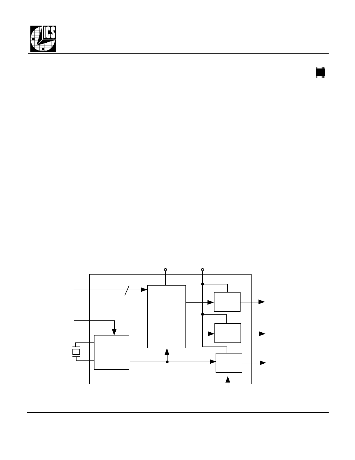
Block Diagram
S1, S0
VIN
10-14 MHz
pullable
crystal
X1
X2
2
Voltage
Controlled
Crystal
Oscillator
PLL/Clock
Synthesis
Circuitry
VDDIOVDD5
Output
Buffer
Output
Buffer
Output
Buffer
OE (all outputs)
CLK1
CLK2
REFCLK
MDS 2732-06 C 1 Revision 120600 Printed 12/21/00
Integrated Circuit Systems • 525 Race Street • San Jose • CA •95126 •(408) 295-9800tel•www.icst.com
Page 2
PRELIMINARY INFORMATION
Low Phase Noise VCXO+Multiplier
MK2732-06
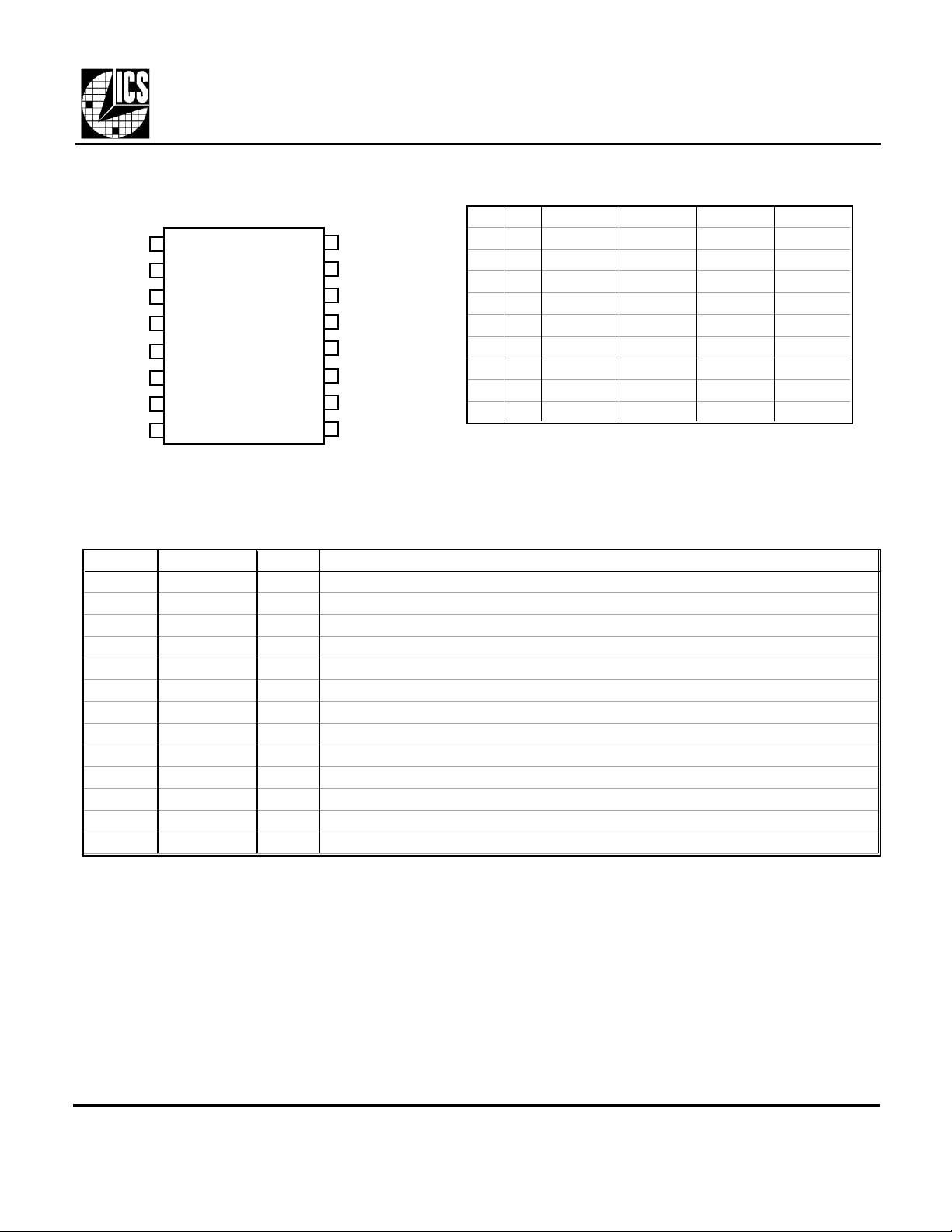
Pin Assignment
Clock Select Table
X1
VDD5
VDD5
VIN
GND
GND
S1
OE
MK2732-06
1
2
3
4
5
6
7
8
16
15
14
13
12
11
10
9
16 pin (173 mil) TSSOP
X2
REFCLK
NC
GND
CLK2
VDDIO
S0
CLK1
S1 S0 Input CLK1 CLK2 Refclk
0 0 13.248 52.992 35.328 off
0 M 13.248 13.248 35.328 off
0 1 13.248 13.248 35.328 on
M 0 13.248 52.992 35.328 on
M M 13.5 54 27 off
M 1 13.5 54 27 on
1 0 13.5 27 54 on
1 M Test mode - - -
1 1 13.5 27 27 on
0=connect directly to GND
M=leave unconnected (floating)
1=connect directly to VDDIO
off=output stopped low.
Pin Descriptions
Number Name Type Description
1 X1 XI Crystal connection. Connect to a pullable crystal of 10-14.318 MHz.
2, 3 VDD5 P Core VDD. Connect to +5V.
4 VIN VI Voltage Input to VCXO. Zero to 3V signal which controls the frequency of the VCXO.
5, 6, 13 GND P Connect to ground.
7 S1 TI Select input #1. Selects outputs per table above. Do not exceed VDDIO.
8 OE I Output Enable. Tri-states outputs when low. Do not exceed VDDIO.
9 CLK1 O Clock Output #1 per table above. Amplitude = VDDIO.
10 S0 TI Select input #0. Selects outputs per table above. Do not exceed VDDIO.
11 VDDIO P Input and output VDD. Connect to +3.3V or +5V. Clock amplitude matches this voltage.
12 CLK2 O Clock Output #2 per table above. Amplitude = VDDIO.
14 NC - Nothing is connected internally to this pin.
15 REFCLK O Buffered crystal VCXO clock
16 X2 XO Crystal connection. Connect to a pullable crystal of 10-14 MHz.
Key: I = Input; TI = tri-level input; O = output; P = power supply connection; VI = analog voltage input;
XI, XO = crystal pins.
External Components
The MK2732-06 requires a minimum number of external components for proper operation. Decoupling
capacitors of 0.01µF should be connected between VDD5 and GND on pins 3 and 5, and VDDIO and
GND on pins 11 and 13, as close to the MK2732-06 as possible. A series termination resistor of 33 Ω may
be used for each clock output. The input crystal must be connected as close to the chip as possible. The
input crystal should be a fundamental mode, parallel resonant, pullable, AT cut. A crystal with 14 pF load
capacitance is recommended. Consult ICS/MicroClock for recommended suppliers. IMPORTANT consult the application note MAN05 for layout guidelines.
MDS 2732-06 C 2 Revision 120600 Printed 12/21/00
Integrated Circuit Systems • 525 Race Street • San Jose • CA •95126 •(408) 295-9800tel•www.icst.com
Page 3

PRELIMINARY INFORMATION
ABSOLUTE MAXIMUM RATINGS (note 1)
DC CHARACTERISTICS (VDD5 = 5.0V, VDD3.3 = 3.3V unless noted)
AC CHARACTERISTICS (VDD5 = 5.0V, VDD3.3 = 3.3V unless noted)
exposure to levels above the operating limits but below the Absolute Maximums may affect device reliability.
2. With an ICS/MicroClock approved pullable crystal.
MK2732-06
Low Phase Noise VCXO+Multiplier
Electrical Specifications
Parameter Conditions Minimum Typical Maximum Units
Supply voltage, VDD Referenced to GND 7 V
Inputs and Clock Outputs Referenced to GND -0.5 VDD+0.5 V
Ambient Operating Temperature 0 70 C
Ambient Operating Temperature, MK2732-06GI
Soldering Temperature Max of 10 seconds 260 C
Storage temperature -65 150 C
Core Operating Voltage, VDD5 4.75 5.0 5.25 V
I/O Operating Voltage, VDDIO 3.13 3.3 5.25 V
Input High Voltage, VIH, X1 pin only 3.5 2.5 V
Input Low Voltage, VIL, X1 pin only 2.5 1.5 V
Input High Voltage, VIH, binary input OE 2 V
Input Low Voltage, VIL, binary input OE 0.8 V
Input High Voltage, VIH, trinary inputs S1, S0 VDD-0.5 V
Input Low Voltage, VIL, trinary inputs S1, S0 0.5 V
Output High Voltage, VOH IOH=-25mA 2.4 V
Output Low Voltage, VOL IOL=25mA 0.4 V
Output High Voltage, VOH, CMOS level IOH=-8mA VDD-0.4 V
Operating Supply Current, IDD No Load 23 mA
Operating Supply Current, IDDIO No Load 5.8 mA
Short Circuit Current Each output ±100 mA
Input Capacitance S1, S0, OE 7 pF
Frequency synthesis error All clocks 0 ppm
VIN, VCXO control voltage 0 3 V
Industrial Temperature -40 85 C
Input Crystal Frequency 10 14 MHz
Output Clock Rise Time 0.8 to 2.0V 1.5 ns
Output Clock Fall Time 2.0 to 0.8V 1.5 ns
Output Clock Duty Cycle At VDDIO/2 40 60 %
Maximum Absolute Jitter, short term ±150 ps
Phase Noise, relative to carrier 10 kHz offset -115 dBc/Hz
Output pullability, note 2 0V ≤ VIN ≤ 3V ±100 ppm
Notes: 1. Stresses beyond those listed under Absolute Maximum Ratings could cause permanent damage to the device. Prolonged
MDS 2732-06 C 3 Revision 120600 Printed 12/21/00
Integrated Circuit Systems • 525 Race Street • San Jose • CA •95126 •(408) 295-9800tel•www.icst.com
Page 4

PRELIMINARY INFORMATION
Millimeters
Low Phase Noise VCXO+Multiplier
MK2732-06
Package Outline and Package Dimensions
E H
h x 45°
D
Q
e
b
c
L
16 pin TSSOP
Symbol Min Max
A - 1.10
b 0.19 0.30
c 0.09 0.20
D 4.90 5.10
E 4.30 4.50
H
e
L 0.50 0.70
Q 0.05 0.15
A
Ordering Information
Part/Order Number Marking Shipping packaging Temperature
MK2732-06G ICS (top line) tubes 16 pin TSSOP 0 to 70 °C
MK2732-06GTR MK27326 (2nd line) tape and reel 16 pin TSSOP 0 to 70 °C
MK2732-06GI ICS (top line) tubes 16 pin TSSOP -40 to -85 °C
MK2732-06GITR MK27326I (2nd line) tape and reel 16 pin TSSOP -40 to -85 °C
Revision history:
Version Revision Comments
A 031199 Original
B 040699 Corrected typo on package width from 73 to 173 mil. Added IDDIO, IDD, jitter. Changed 1M selection
to Test Mode. Changed aspect ratio of pinout package. Changed features to show xDSL and MPEG.
C 120600 Added Industrial Temperature version of device (MK2732-06GI and MK2732-06GITR)
While the information presented herein has been checked for both accuracy and reliability, Integrated Circuit Systems, Incorporated (ICS) assumes no responsibility for either its
use or for the infringement of any patents or other rights of third parties, which would result from its use. No other circuits, patents, or licenses are implied. This product is
intended for use in normal commercial applications. Any other applications such as those requiring extended temperature range, high reliability, or other extraordinary
environmental requirements are not recommended without additional processing by ICS. ICS reserves the right to change any circuitry or specifications without notice. ICS does
not authorize or warrant any ICS product for use in life support devices or critical medical instruments.
MDS 2732-06 C 4 Revision 120600 Printed 12/21/00
Integrated Circuit Systems • 525 Race Street • San Jose • CA •95126 •(408) 295-9800tel•www.icst.com
 Loading...