

Page 1
MK2731-03C
MPEG Audio Clock Synthesizer
Description
The MK2731-03 is a low cost, low jitter, high
performance PLL clock synthesizer designed to
replace oscillators and PLL circuits in set-top box
and multimedia systems. Using our proprietary
analog Phase-Locked Loop (PLL) techniques, the
device uses an inexpensive crystal or clock input to
produce up to three output clocks. All of the audio
frequencies are synthesized exactly, with zero ppm
error, and locked to the 27 MHz clock.
MicroClock manufactures the largest variety of
Set-Top Box and multimedia clock synthesizers
for all applications. Consult MicroClock to
eliminate VCXOs, crystals and oscillators from
your board.
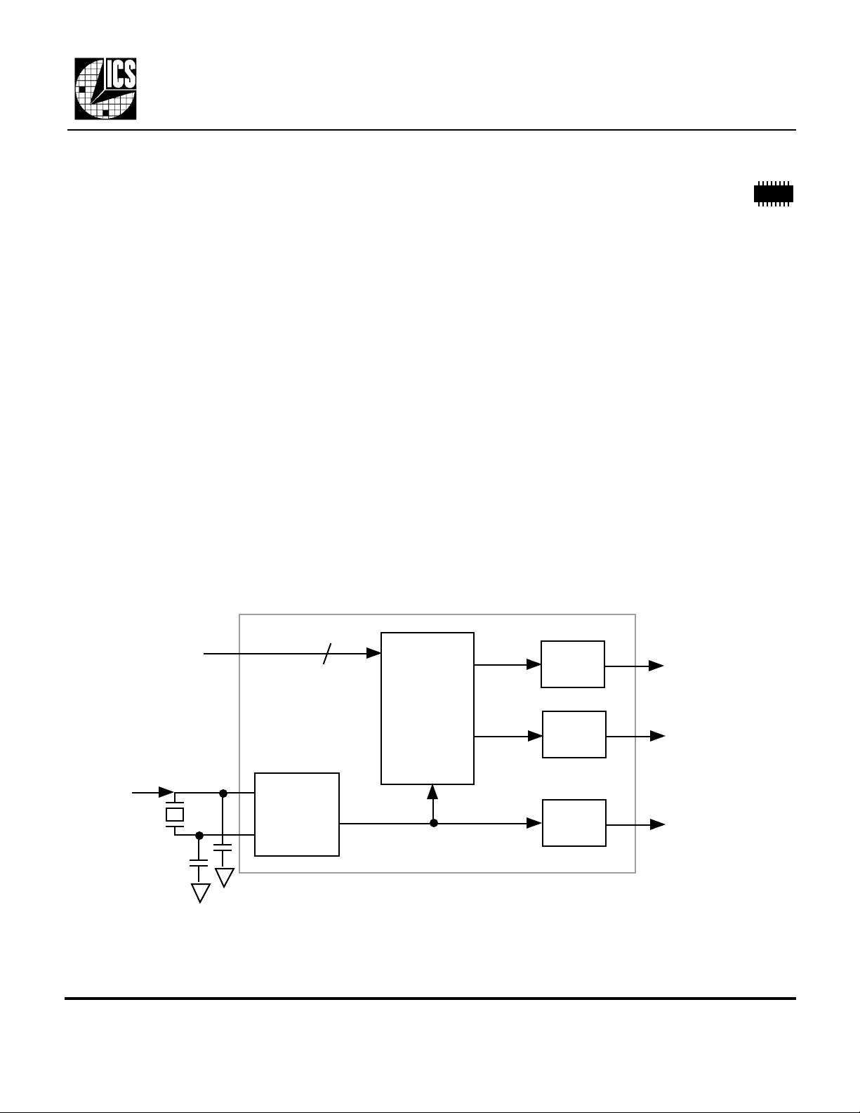
Block Diagram
Features
• Packaged in 16 pin narrow SOIC
• Produces exact audio clocks from the video
• Uses a crystal or clock input
• Zero ppm synthesis error in all clocks
• All frequencies are frequency locked
• 25mA output drive capability at TTL levels
• Advanced, low power, sub-micron CMOS process
• 3.3V or 5V operating voltage
Crystal
3
PLL/Clock
Synthesis
Circuitry
Output
Buffer
Output
Buffer
Output
Buffer
CLK1
CLK2
REF
S2:0
27 MHz crystal
or clock
(Capacitors are required
for crystal tuning)
MDS 2731-03C D 1 Revision 011101
Integrated Circuit Systems, Inc.• 525 Race Street, San Jose, CA, 95126 • (408) 295-9800 tel • www.icst.com
X1
Oscillator
X2
Page 2
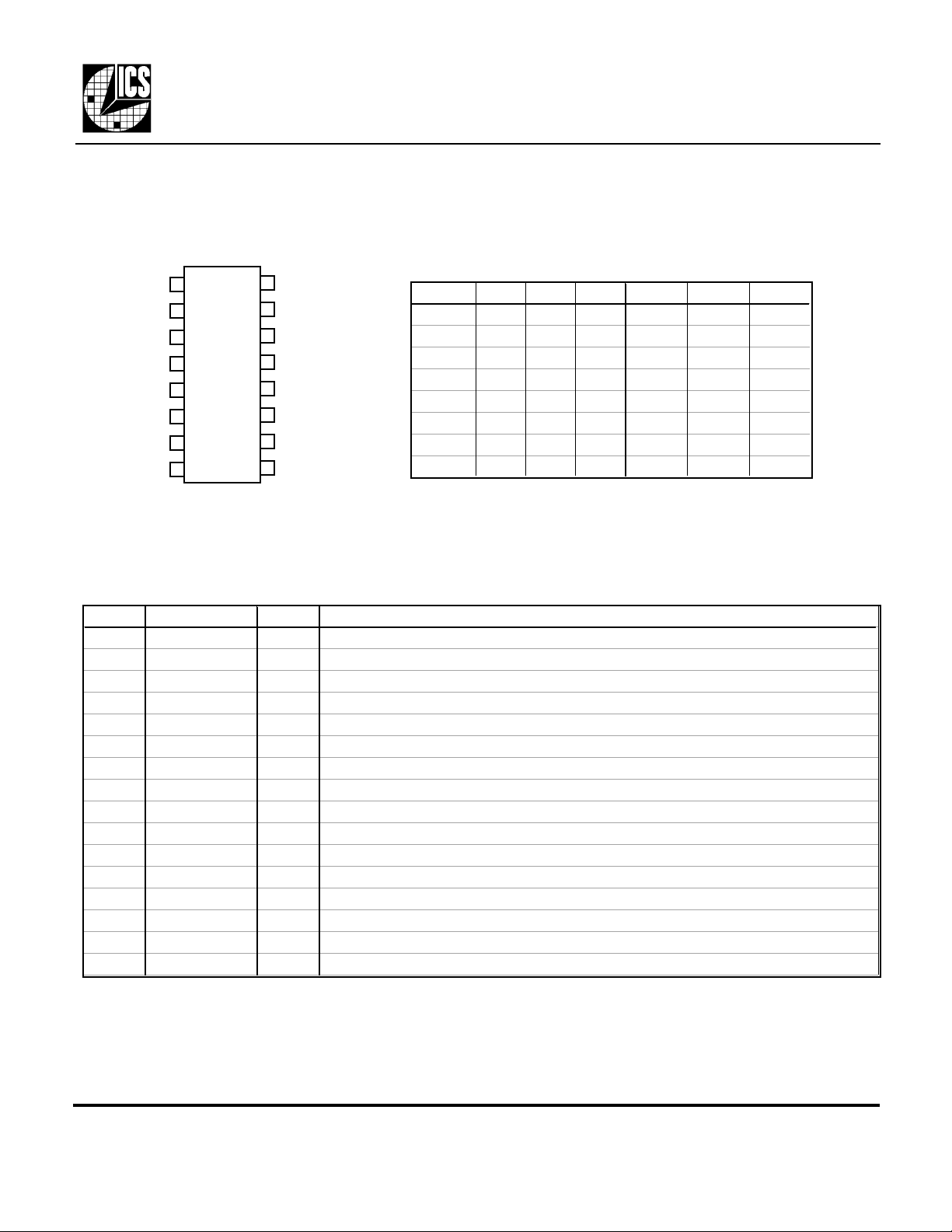
Pin Assignment
MK2731-03C
MPEG Audio Clock Synthesizer
MK2731-03C
Output Clock Select Table (MHz)
16
X2
X1
VDD
VDD
GND
GND
S2
GND
1
2
3
4
5
6
7
8
16 pin narrow (150 mil) SOIC
Pin Descriptions
Number Name Type Description
1 X2 XO Crystal connection to a 27 MHz fundamental crystal. Leave unconnected for clock input.
2 X1 XI Crystal connection to a 27 MHz fundamental crystal. Can also be connected to input clock.
3 VDD P VDD. Connect to VDD.
4 VDD P VDD. Connect to VDD.
5 GND P Connect to ground.
6 GND P Connect to ground.
7 S2 I Clock Select 2. Selects outputs per table above.
8 GND P Connect to ground.
9 DC - Do not connect anything to this pin.
10 CLK1 O Clock output 1 determined by status of S2, S1, S0. See table above.
11 S1 I Clock Select 1. Selects outputs per table above.
12 NC - No Connect. Nothing is connected internally to this pin.
13 S0 I Clock Select 0. Selects outputs per table above.
14 CLK2 O Clock output 2 determined by status of S2, S1, S0. See table above.
15 NC - No Connect. Nothing is connected internally to this pin.
16 REF O Reference crystal output or off. See table above.
15
14
13
12
11
10
REF
NC
CLK2
S0
NC
S1
CLK1
DC
9
Input S2 S1 S0 CLK1 CLK2 REF
27 0 0 0 Off 8.192 Off
27 0 0 1 Off 11.2896 Off
27 0 1 0 Off 12.288 Off
27 0 1 1 Off 24.576 Off
27 1 0 0 4.096 8.192 27
27 1 0 1 5.6448 11.2896 27
27 1 1 0 6.144 12.288 27
27 1 1 1 12.288 24.576 27
Key: 0 = connect pin directly to ground
1 = connect pin directly to VDD
Off = clock stopped low
Key: I = Input, O = output, P = power supply connection
MDS 2731-03C D 2 Revision 011101
Integrated Circuit Systems, Inc.• 525 Race Street, San Jose, CA, 95126 • (408) 295-9800 tel • www.icst.com
Page 3

MK2731-03C
ABSOLUTE MAXIMUM RATINGS (note 1)
DC CHARACTERISTICS (VDD = 5.0V unless noted)
AC CHARACTERISTICS (VDD = 5.0V unless noted)
see table on following page
exposure to levels above the operating limits but below the Absolute Maximums may affect device reliability.
MPEG Audio Clock Synthesizer
Electrical Specifications
Parameter Conditions Minimum Typical Maximum Units
Supply voltage, VDD Referenced to GND 7 V
Inputs and Clock Outputs Referenced to GND -0.5 VDD+0.5 V
Ambient Operating Temperature 0 70 °C
Soldering Temperature Max of 10 seconds 260 °C
Storage temperature -65 150 °C
Operating Voltage, VDD 3.13 5.50 V
Input High Voltage, VIH, X1 pin only (VDD/2)+1 VDD/2 V
Input Low Voltage, VIL, X1 pin only VDD/2 (VDD/2)-1 V
Input High Voltage, VIH 2 V
Input Low Voltage, VIL 0.8 V
Output High Voltage, VOH IOH=-25mA 2.4 V
Output Low Voltage, VOL IOL=25mA 0.4 V
Output High Voltage, VOH, CMOS level IOH=-8mA VDD-0.4 V
Operating Supply Current, IDD No Load 25 mA
Short Circuit Current Each output ±100 mA
Input Capacitance S2, S1, S0 7 pF
Frequency synthesis error All clocks 0 ppm
Input Crystal or Clock Frequency
Input Crystal Accuracy ±30 ppm
Output Clock Rise Time 0.8 to 2.0V 1.5 ns
Output Clock Fall Time 2.0 to 0.8V 1.5 ns
Output Clock Duty Cycle At 1.4V 40 60 %
Maximum Absolute Jitter, short term
Notes: 1. Stresses beyond those listed under Absolute Maximum Ratings could cause permanent damage to the device. Prolonged
27.00
MHz
External Components
The MK2731-03 requires a minimum number of external components for proper operation. Decoupling
capacitors of 0.1µF should be connected between VDD and GND on pins 3 and 5, as close to the
MK2731-03 as possible. A series termination resistor of 33Ω may be used for each clock output. The input
crystal must be connected as close to the chip as possible. The input crystal should be a parallel resonant,
fundamental, AT cut 27 MHz. For accurate tuning of the output when a crystal input is used, capacitors
should be connected between X1 and ground, and X2 and ground. The value of these capacitors is given by
the following equation, where CL is the crystal load capacitance: Crystal caps (pF) = (CL-10) x 2. So for a
crystal with 16 pF load capacitance, two 12 pF caps can be used.
MDS 2731-03C D 3 Revision 011101
Integrated Circuit Systems, Inc.• 525 Race Street, San Jose, CA, 95126 • (408) 295-9800 tel • www.icst.com
Page 4

MK2731-03C
Inches
Millimeters
MPEG Audio Clock Synthesizer
Jitter Measurements
S2 S1 S0 CLK2 5V 3.3V
(MHz) one sigma (ps) typical max (± ps) one sigma (ps) typical max (± ps)
0 0 0 8.192 45 110 92 185
0 0 1 11.2896 25 60 42 110
0 1 0 12.288 24 70 49 130
0 1 1 24.576 32 90 52 150
Notes: 1. Jitter is about equal at 25°C and 70°C
Package Outline and Package Dimensions
E H
INDEX
AREA
1 2
D
A1 C
e
B
Ordering Information
16 pin SOIC narrow
Symbol Min Max Min Max
A 0.0532 0.0688 1.35 1.75
A1 0.0040 0.0098 0.10 0.24
B 0.0130 0.0200 0.33 0.51
C 0.0075 0.0098 0.19 0.24
D 0.3859 0.3937 9.80 10.00
E 0.1497 0.1574 3.80 4.00
e
H 0.2284 0.2440 5.80 6.20
L 0.0160 0.0500 0.41 1.27
A
L
While the information presented herein has been checked for both accuracy and reliability, Integrated Circuit Systems, Incorporated assumes no responsibility for either its use or
for the infringement of any patents or other rights of third parties, which would result from its use. No other circuits, patents, or licenses are implied. This product is intended for
use in normal commercial applications. Any other applications such as those requiring extended temperature range, high reliability, or other extraordinary environmental
requirements are not recommended without additional processing by ICS. ICS reserves the right to change any circuitry or specifications without notice. ICS does not authorize
or warrant any ICS product for use in life support devices or critical medical instruments.
MDS 2731-03C D 4 Revision 011101
Integrated Circuit Systems, Inc.• 525 Race Street, San Jose, CA, 95126 • (408) 295-9800 tel • www.icst.com
Part/Order Number Marking Shipping packaging Package Temperature
MK2731-03S MK2731-03S tubes 16 pin SOIC 0-70 °C
MK2731-03STR MK2731-03S tape and reel 16 pin SOIC 0-70 °C
 Loading...