

Page 1
MK2059-01
VCXO-Based Frame Clock Frequency Translator
Description
The MK2059-01 is a VCXO (V oltage Controlled Crystal
Oscillator) based clock generator that produces
common telecommunications reference frequencies.
The output clock is phase locked to an 8kHz (frame
rate) input reference clock. The MK2059-01 also
provides jitter attenuation. Included in the selection of
output frequencies are these common system clocks:
1.544 MHz (T1) 2.048 (E1)
19.44 MHz (OC-3) 16.384 MHz (8x E1)
This monolithic IC, combined with an external
inexpensive quartz crystal, can be used to replace a
more costly hybrid VCXO retiming module. Through
selection of external loop filter components, the PLL
loop bandwidth and damping factor can be tailored to
meet input clock jitter attenuation requirements. A loop
bandwidth down to the Hz range is possible.
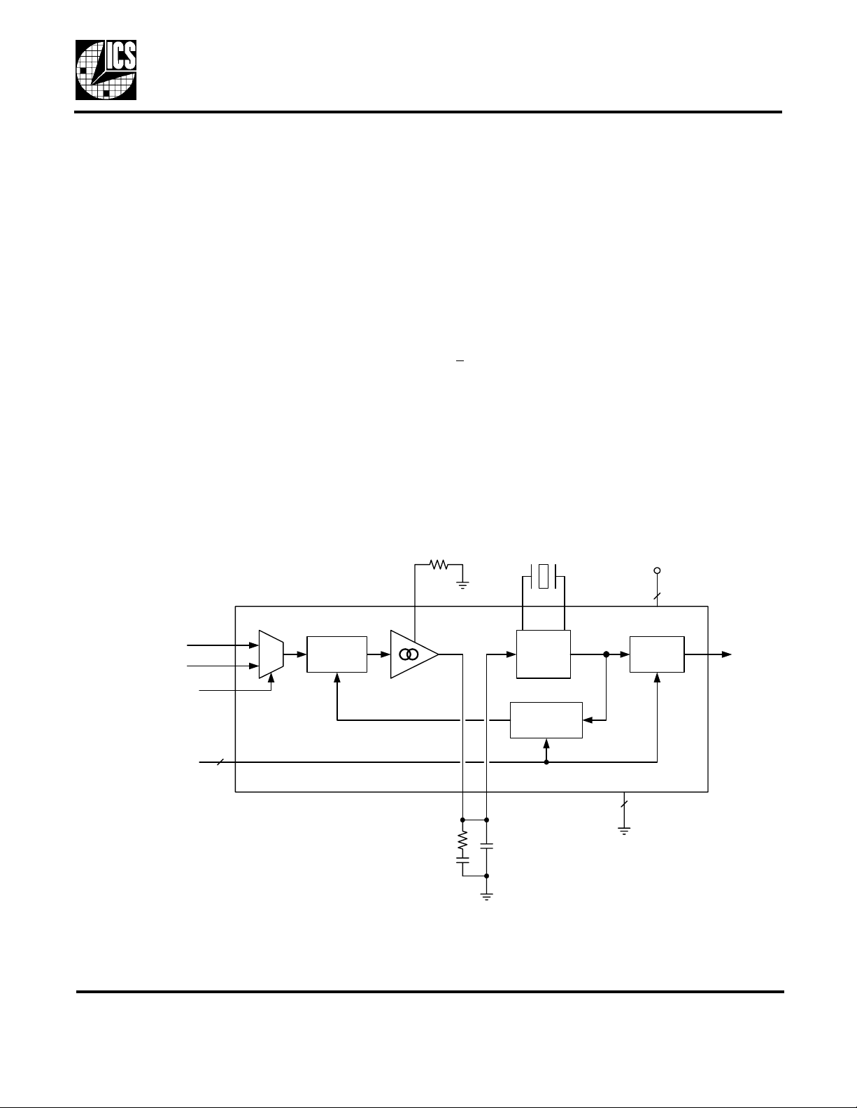
Block Diagram
Features
• Generates T1, E1, OC-3 and other common telecom
clock frequencies from an 8kHz frame clock
• Configurable jitter attenuation characterisitics,
excellent for use as a Stratum source de-jitter circuit
• 2:1 Input MUX for input reference clocks
• VCXO-based clock generation offers very low jitter
and phase noise generation
• Output clock is phase and frequency locked to the
selected input reference clock
• Fixed input to output phase relationship
• +115ppm minimum crystal frequency pullability
range, using recommended crystal
• Industrial temperature range
• Low power CMOS technology
• 20 pin SOIC package
• Single 3.3V power supply
Pullable xtal
VDD
8kHz Ref Input
8kHz Ref Input
ISEL
SEL2:0
ICLK2
ICLK1
ISET
1
0
3
Phase
Detector
Charge
Pump
CHGP
VCXO
Feedback
Divider
VIN
X2X1
GND
VDD
Output
Divider
4
3
CLK
MDS 2059-01 B 1 Revision 071001
Integrated Circuit Systems, Inc. ● 525 Race Street, San Jose, C A 95126 ● tel (408) 295-9 800 ● www.icst.com
Page 2
MK2059-01
VCXO-Based Frame Clock Frequency Translator
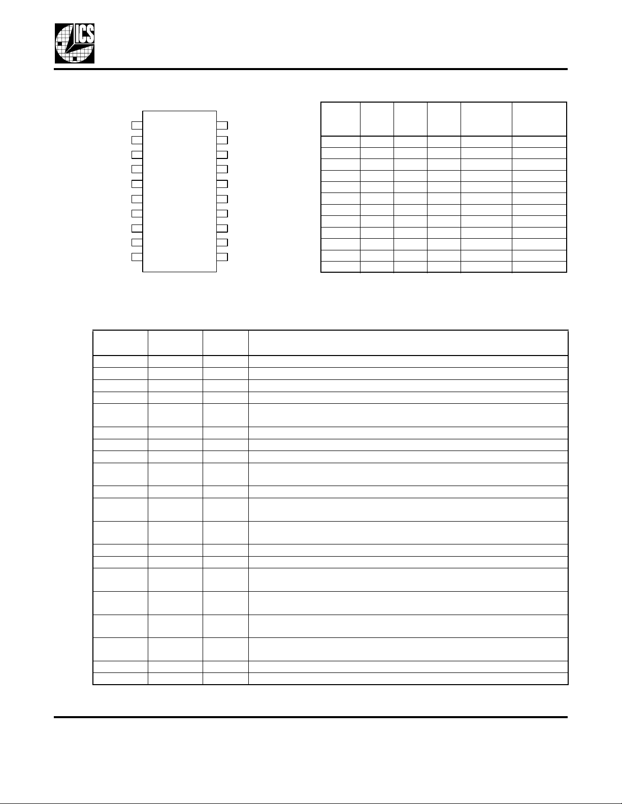
Pin Assignment
X1 X2
VDD
VDD
VDD
VIN
GND
GND
GND
CHGP
ISE T
1
2
3
4
5
6
7
8
9
10
20 pin 300 mil SOIC
Pin Descriptions
Pin
Number
1 X1 - Crystal Input. Connect this pin to the specified crystal.
2 VDD Power Power Supply. Connect to +3.3V.
3 VDD Power Power Supply. Connect to +3.3V.
4 VDD Power Power Supply. Connect to +3.3V.
5 VIN Input VCXO Control Voltage Input. Connect this pin to CHGP pin and the external
6 GND Power Connect to ground
7 GND Power Connect to ground
8 GND Power Connect to ground
9 CHGP Output Charge Pump Output. Connect this pin to the external loop filter and to pin
10 ISET - Charge pump current setting node, connection for setting resistor.
11 SEL2 Input Output Frequency Selection Pin 2. Determines output frequency as per table
12 SEL1 Input Output Frequency Selection Pin 1. Determines output frequency as per table
13 NC Input No Internal Connection.
14 CLK Output Clock Ou tput
15 SEL0 Input Output Frequency Selection Pin 0. Determines output frequency as per table
16 ICLK2 Input Input Clock Connection 2. Connect an input reference clock to this pin. If
17 ICLK1 Input Input Clock Connection 1. Connect an input reference clock to this pin. If
18 ISEL Input Input Selection. Used to select which refere nce input c lock is ac tive. Low inpu t
19 GND Power Connect to ground.
20 X2 - Crystal Output. Connect this pin to the specified crystal.
Pin
Name
20
19
18
17
16
15
14
13
12
11
Pin
Type
Output Clock Selection Table
Output
Input SEL2 SEL1 SEL0
GND
ISEL
IC L K1
IC L K2
SEL0
CLK
NC
SEL1
SEL2
8 kHz 0 0 0 1.544 24.704
8 kHz 0 0 1 2.048 24.576
8 kHz 0 1 0 16.384 16.384
8 kHz 0 1 1 17.664 17.664
8 kHz M 0 0 18.528 18.528
8 kHz M 0 1 20.00 20.00
8 kHz M 1 0 25.00 25.00
8 kHz M 1 1 25.92 25.92
8 kHz 1 0 0 19.44 19.44
8 kHz 1 0 1 20.48 20.48
8 kHz 1 1 0 24.704 24.704
8 kHz 1 1 1 24.576 24.576
Note: For SEL input pin programming:
0 = GND, 1 = VDD, M = Floating
Pin Description
loop filter as shown in this data sheet.
VIN.
above. Internally biased to VDD/2.
above. Internal pull-up.
above. Internal pull-up.
unused, connect to ground.
unused, connect to ground.
level selects ICLK1, high input level selects ICLK2. Internal pull-up.
Clock
(MHz)
Crystal
Used (MHz)
MDS 2059-01 B 2 Revision 071001
Integrated Circuit Systems, Inc. ● 525 Race St reet, San Jose, CA 9512 6 ● tel (408) 295-9800 ● www.icst.com
Page 3

VCXO-Based Frame Clock Frequency Translator
MK2059-01
Functional Description
The MK2059-01 is a clock generator IC that generates
an output clock directly from an internal VCXO circuit
which works in conjunction with an external quartz
crystal. The VCXO is controlled by an internal PLL
(Phase Locked Loop) circuit, enabling the device to
perform clock regeneration from an input reference
clock. The MK2059-01 is configured to provide a MHz
communications reference clock output from an 8kHz
input clock. There are 12 selectable output
frequencies. Please refer to the Output Clock Selection
Table on Page 2.
Most typical PLL clock devices use an internal VCO
(Voltage Controlled Oscillator) for output clock
generation. By using a VCXO with an external crystal,
the MK2059-01 is able to generate a low jitter, low
phase-noise output clock within a low bandwidth PLL.
This serves to provide input clock jitter attenuation and
enables stable operation with a low frequency
reference clock.
The VCXO circuit requires an external pullable crystal
for operation. External loop filter components enable a
PLL configuration with low loop band wid th.
Application Information
Quartz Crystal
It is important that the correct type of quartz crystal is
used with the MK2059-01. Failure to do so may result
in reduced frequency pullability range, inability of the
loop to lock, or excessive output phase jitter.
The MK2059-01 operates by phase-locking the VCXO
circuit to the input signal of the selected ICLK input.
The VCXO consists of the external crystal and the
integrated VCXO oscill ator circuit. To achieve the best
performance and reliability, a crystal device with the
recommended parameters (shown bel ow) must be
used, and the layout guidelines discussed in the PCB
Layout Recommendations section must be followed.
The frequency of oscillation of a quartz crystal is
determined by its cut and by the external load
capacitance. The MK2059-01 incorporates variable
load capacitors on-chip which “pull”, or change, the
frequency of the crystal. The crystals specified for use
with the MK2059-01 are designed to have zero
frequency error when the total of on-chip + stray
capacitance is 14pF. To achieve this, the layout should
use short traces between the MK2059-01 and the
crystal.
A complete description of the recommended crystal
parameters is shown below.
Recommended Crystal Parameters:
Output Frequency Configuration
The MK2059-01 is configured to generate a set of
output frequencies from an 8kHz input clock. Please
refer to the Output Clock Selection Table on Page 2.
Input bits SEL2:0 are set according to this table, as is
the external crystal frequency. Please refer to the
Quartz Crystal section on this page regarding external
crystal requirements.
Input Mux
The Input Mux serves to select between two alternate
input reference clocks. Upon reselection of the input
clock, clock glitches on the output clock will not be
generated due to the “fly-wheel” effect of the VCXO
(the quartz crystal is a high-Q tuned circuit). When the
input clocks are not phase aligned, the phase of the
output clock will change to reflect the phase of newly
selected input at a controlled phase slope (rate of
phase change) as influenced by the PLL loop
characteristics.
MDS 2059-01 B 3 Revision 071001
Operating Temperature Range
Commercial Applications 0 to 70
Industrial Applications -40 to 85
Initial Accuracy at 25
Temperature Stability ±30 ppm
Aging ±20 ppm
Load Capacitance Note 1
Shunt Capacitance, C0 7 pF Max
C0/C1 Ratio 250 Max
Equivalent Series Resistance 35 Ω Max
Note 1: For crystal frequencies between 13.5MHz and
27MHz the nominal crystal load capacitance
specification should be 14pF. Contact ICS MicroClock
applications at (408) 297-1201 regarding the use of a
crystal below 13.5MHz.
To obtain a list of qualified crystal devices that meet
these requirements, please contact ICS MicroClock
applications department.
°C ±20 ppm
°C
°C
Integrated Circuit Systems, Inc. ● 525 Race St reet, San Jose, CA 9512 6 ● tel (408) 295-9800 ● www.icst.com
Page 4

MK2059-01
VCXO-Based Frame Clock Frequency Translator
PLL Loop Filter Components
All analog PLL circuits use a loop filter to establish
operating stability. The MK2059-01 uses external loop
filter components for the following reasons:
1) Larger loop filter capacitor values can be used,
allowing a lower loop bandwidth. This enables the use
of lower input clock reference frequencies and also
input clock jitter attenuation capabilities. Larger loop
filter capacitors also allow higher loop damping factors
when less passband peaking is desired.
2) The loop filter values can be user selected to
optimize loop response characteristics for a given
application.
Referencing the External Component Schematic on
this page, the external loop filter is made up of
components R
, C1 and C2. R
Z
charge pump current and therefore influences loop
filter characteristics.
establishes PLL
SET
External Compon ent Schematic
C
L
Don’t Stuff
(Re fe r to Optio n a l
Crystal Tuning
section)
C
2
X1 X2
VDD
VDD
VDD
VIN
GND
R
Z
GND
GND
C
1
CHGP
ISET
R
Xtal
1
2
3
4
5
6
7
8
9
10
SET
20
19
18
17
16
15
14
13
12
11
C
L
GND
ISEL
ICLK1
ICLK2
SEL0
CLK
NC
SEL1
SEL2
Recommended Loop Filter Values Vs. Output Frequency Range Selection
Crystal
SEL2 SEL1 SEL0
Multiplier
(N)
0 0 0 3088 120 k
0 0 1 3072 120 k
0 1 0 2048 120 k
0 1 1 2208 120 k
M 0 0 2316 120 k
M 0 1 2500 120 k
M 1 0 3125 120 k
M 1 1 3240 120 k
1 0 0 2430 120 k
1 0 1 2560 120 k
1 1 0 3088 120 k
1 1 1 3072 120 kΩ 1.0 MΩ 0.1 µF 4.7 nF 19 Hz 1.4
Note: For SEL input pin programming: 0 = GND, 1 = VDD, M = Floating
R
SET
R
Z
C1 C2Loop
Bandwidth
(-3dB point)
1.0 M
Ω
1.0 M
Ω
1.0 M
Ω
1.0 M
Ω
1.0 M
Ω
1.0 M
Ω
1.0 M
Ω
1.0 M
Ω
1.0 M
Ω
1.0 M
Ω
1.0 M
Ω
0.1 µF 4.7 nF 18 Hz 1.4
Ω
0.1 µF 4.7 nF 19 Hz 1.4
Ω
0.1 µF 4.7 nF 27 Hz 1.7
Ω
0.1 µF 4.7 nF 26 Hz 1.7
Ω
0.1 µF 4.7 nF 24 Hz 1.6
Ω
0.1 µF 4.7 nF 22 Hz 1.6
Ω
0.1 µF 4.7 nF 18 Hz 1.4
Ω
0.1 µF 4.7 nF 17 Hz 1.4
Ω
0.1 µF 4.7 nF 23 Hz 1.6
Ω
0.1 µF 4.7 nF 22 Hz 1.6
Ω
0.1 µF 4.7 nF 18 Hz 1.4
Ω
Damping
Factor
MDS 2059-01 B 4 Revision 071001
Integrated Circuit Systems, Inc. ● 525 Race St reet, San Jose, CA 9512 6 ● tel (408) 295-9800 ● www.icst.com
Page 5

NBW
R
ZICP
× 575×
N
----------------------------------------=
MK2059-01
VCXO-Based Frame Clock Frequency Translator
A “normalized” PLL loop bandwidth may be calculated
as follows:
The “normalized” bandwidth equation above does not
take into account the effects of damping factor or the
second pole. However, it does provide a useful
approximation of filter performance.
The loop damping factor is calculated as follows:
Damping Factor R
=
625 ICP×
×
-----------------------------------------
Z
C
×
1
N
Where:
= Value of resistor in loop filter (Ohms)
R
Z
= Charge pump current (amps)
I
CP
(refer to Charge Pump Current Table, below)
N = Crystal multiplier shown in the above table
= Value of capacitor C1 in loop filter (Farads)
C
1
As a general rule, the following relationship should be
maintained between components C
and C2 in the loop
1
filter:
C
1
C
----- -
=
2
20
Charge Pump Current Table
Charge Pump Current
R
SET
1.4 MΩ 10 µA
680 kΩ 20 µA
540 kΩ 25 µA
120 kΩ 100 µA
(I
)
CP
1) The loop capacitors should be a low-leakage type to
avoid leakage-induced phase noise. For this reason,
DO NOT use any type of polarized or electrolytic
capacitors.
2) Microphonics (mechanical board vibration) can also
induce output phase noise, especially when the loop
bandwidth is less than 1kHz. For this reason, ceramic
capacitors should have C0G or NP0 dielectric. Avoid
high-K dielectrics like Z5U and X7R. These and some
other ceramics have piezoelectric properties that
convert mechanical vibration into voltage noise that
interferes with VCXO operation.
For larger loop capacitor values such as 0.1 µF or 1 µF,
PPS film types made by Panasonic, or metal poly types
made by Murata or Cornell Dubilier are recommended.
For questions or changes regarding loop filter
characteristics, please contact your sales area FAE, or
ICS MicroClock Applications.
Series Termination Resistor
Clock output traces over one inch should use series
termination. To series terminate a 50Ω trace (a
commonly used trace impedance), place a 33Ω resistor
in series with the clock line, as close to the clock output
pin as possible. The nominal impedance of the clock
output is 20Ω. (The optional series termination resistor
is not shown in the External Component Schematic.)
Decoupling Capacitors
As with any high performance mixed-signal IC, the
MK2059-01 must be isolated from system power
supply noise to perform optimally.
Decoupling capacitors of 0.01µF must be connected
between each VDD and the PCB ground plane. To
further guard against interfering system supply noise,
the MK2059-01 should use one common connection to
the PCB power plane as shown in the diagram on the
next page. The ferrite bead and bulk capacitor help
reduce lower frequency noise in the supply that can
lead to output clock phase modulation.
Special considerations must be made in choosing loop
components C
MDS 2059-01 B 5 Revision 071001
Integrated Circuit Systems, Inc. ● 525 Race St reet, San Jose, CA 9512 6 ● tel (408) 295-9800 ● www.icst.com
and C2:
1
Page 6

Connection to 3.3V
Power Plane
Ferrite
Bead
Bulk Decoupling Capacitor
(such as 1
µF Tantalum)
VDD Pin
VDD Pin
VDD Pin
0.01
µF D eco upling Capac itors
MK2059-01
VCXO-Based Frame Clock Frequency Translator
Recommended Power Supply Connection
for Optimal Device Performance
Crystal Load Capacitors
The device crystal connections should include pads for
small capacitors from X1 to ground and from X2 to
ground, shown as C
Schematic. These capacitors are used to adjust the
stray capacitance of the board to match the nominally
required crystal load capacitance. Because load
capacitance can only be increased in this trimming
process, it is important to keep stray capacitance to a
minimum by using very short PCB traces (and no via’s)
been the crystal and device.
In most cases the load capacitors will not be required.
They should not be stuffed on the prototype evaluation
board as the indiscriminate use of these trim capacitors
will typically cause more crystal centering error than
their absence. If the need for the load capacitors is later
determined, the values will fall within the 1-4 pf range.
The need for, and value of, these trim capacitors can
only be determined at prototype evaluation. Please
refer to the Optimization of Crystal Load Capacitors
section for more information.
PCB Layout Recommendations
For optimum device performance and lowest output
phase noise, the following guidelines should be
observed. Pl ease als o refe r to the Re commend ed PCB
Layout drawing on Page 7.
1) Each 0.01µF decoupling capacitor should be
mounted on the component side of the board as close
to the VDD pin as possible. No via’s should be used
between decoupling capacitor and VDD pin. The PCB
trace to VDD pin should be kept as short as possible,
MDS 2059-01 B 6 Revision 071001
Integrated Circuit Systems, Inc. ● 525 Race St reet, San Jose, CA 9512 6 ● tel (408) 295-9800 ● www.icst.com
in the External Component
L
as should the PCB trace to the ground via. Distance of
the ferrite bead and bulk decoupling from the device is
less critical.
2) The loop filter components must also be placed
close to the CHGP and VIN pins. C
should be closest
2
to the device. Coupling of noise from other system
signal traces should be minimized by keeping traces
short and away from active signal traces. Use of vias
should be avoided.
3) The external crystal should be mounted just next to
the device with short traces. The X1 and X2 traces
should not be routed next to each other with minimum
spaces, instead they should be separated and away
from other traces.
4) T o minimize EMI the 33Ω series termination resistor ,
if needed, should be placed close to the clock output.
5) An optimum layout is one with all components on the
same side of the board, minimizing vias through other
signal layers (the ferrite bead and bulk decoupling
capacitor can be mounted on the back). Other signal
traces should be routed away from the MK2059-01.
This includes signal traces just underneath the device,
or on layers adjacent to the ground plane layer used by
the device.
The ICS Applications Note MAN05 may also be
referenced for additional suggestions on layout of the
crystal section.
Optimization of Crystal Load Capacitors
The concept behind the optional crystal load capacitors
was introduced previously in this data sheet (see
Crystal Load Capacitor section on Page 5). To
determine the need for and value of these capacitors,
you will need a PCB of your final layout, a frequency
counter capable of less than 10 ppm resolution and
accuracy, two power supplies, and some samples of
the crystals which you plan to use in production, along
with measured initial accuracy for each crystal at the
specified crystal load capaci tance, CL.
To determine the value of the crystal capacitors:
1. Connect VDD to 3.3V. Connect pin 5 to the second
power supply. Adjust the voltage on pin 5 to 0V.
Measure and record the frequency of the CLK output.
Page 7

Error 106x
f
3.0Vftetarg
–()f0Vf
tetarg
–()+
f
tetarg
------------------------------------------------------------------------------
error
xtal
–=
MK2059-01
VCXO-Based Frame Clock Frequency Translator
2. Adjust the voltage on pin 5 to 3.3V. Measure and
record the frequency of the same output.
To calculate the centering error:
Where:
= nominal crystal frequency
f
target
error
=actual initial accuracy (in ppm) of the crystal
xtal
being measured
If the centering error is less than ±15 ppm, adjustment
is not needed for most applications. If the cente ring
error is more than 15 ppm negative, the PCB has too
Recommended PCB Layout
much stray capacitance and will need to be redone with
a new layout to reduce stray capacitance. Alternately,
the crystal may be re-specified for a higher lower load
capacitance. Contact ICS MicroClock for details. If the
centering error is more than 15 ppm positive, add
identical fixed centering capacitors from each crystal
pin to ground. The value for each of these caps (in pF)
is given by:
External Capacitor =
2 x (centering error)/(trim sensitivity)
Trim sensitivity is a parameter which can be supplied
by your crystal vendor. If you do not know the value,
assume it is 30 ppm/pF. After any changes, repeat the
measurement to verify that the remaining error is
acceptably low (less than ±15ppm).
For minimum ou tput clock jitter,
device VDD conne ctions should
be made to comm on bulk
decoupling device (see text).
G
G
G
G
1
2
3
4
5
G
6
7
8
G
G
9
G
10
G
20
G
19
18
17
16
15
14
13
12
11
For minimum ou tput clock jitter,
remove ground and power plane
within th is e n tire a rea . A lso ro u te
all other traces away from this area.
NC
Legend:
G
= Ground
Co n n ec tion
MDS 2059-01 B 7 Revision 071001
Integrated Circuit Systems, Inc. ● 525 Race St reet, San Jose, CA 9512 6 ● tel (408) 295-9800 ● www.icst.com
Page 8

Absolute Maximum Ratings
Stresses above the ratings listed below can cause permanent damage to the MK2059-01. These ratings,
which are standard values for ICS commercially rated parts, are stress ratings only . Functional operation of
the device at these or any other conditions above those indicated in the operational sections of the
specifications is not implied. Exposure to absolute maximum rating conditions for extended periods can
affect product reliability. Electrical parameters are guaranteed only over the recommended operating
temperature range.
Item Rating
Supply Voltage, VDD 7V
All Inputs and Outputs -0.5V to VDD+0.5V
Ambient Operating Temperature -40 to +85°C
Storage Temperature -65 to +150°C
Junction Temperature 175°C
Soldering Te mpe ra ture 260°C
MK2059-01
VCXO-Based Frame Clock Frequency Translator
Recommended Operation Conditions
Parameter Min. Typ. Max. Units
Ambient Operating Temperature -40 – +85
Power Supply Voltage (measured in respect to GND) +3.15 +3.3 +3.45 V
DC Electrical Characteristics
Unless stated otherwise, VDD = 3.3V ±5%, Ambient Temperature -40 to +85°C
Parameter Symbol Conditions Min. Typ. Max. Units
Operating Voltage VDD 3.15 3.3 3.45 V
Supply Current IDD Clock outputs
unloaded, VDD = 3.3V
Input High Voltage, SEL2 V
Input Low Voltage, SEL2 V
Input High Voltage, ISEL,
SEL1:0
Input Low Voltage, ISEL,
SEL1:0
Input High Voltage, ICLK1, 2 V
Input Low Voltage, ICLK1, 2 V
Input High Current I
Input Low Current I
Input Capacitance, except X1 C
IH
IL
V
IH
V
IL
IH
IL
IH
IL
V
IH
V
IL
IN
C
°
10 15 mA
–VDD-0.5––V
–––0.5V
–2––V
–––0.8V
–
–––
VDD/2+1
––V
VDD/2-1
V
= VDD -10 – +10 µA
= 0 -10 – +10 µA
––7–pF
MDS 2059-01 B 8 Revision 071001
Integrated Circuit Systems, Inc. ● 525 Race St reet, San Jose, CA 9512 6 ● tel (408) 295-9800 ● www.icst.com
Page 9

Parameter Symbol Conditions Min. Typ. Max. Units
Output High Voltage (CMOS
Level)
Output High Voltage V
Output Low Voltage V
Short Circuit Current I
VIN, VCXO Control Voltage V
Nominal Output Impedance Z
AC Electrical Characteristics
Unless stated otherwise, VDD = 3.3V ±5%, Ambient Temperature -40 to +85° C
Parameter Symbol Conditions Min. Typ. Max. Units
VCXO Crystal Pull Range f
VCXO Crystal Nominal
Frequency
Input Jitter Tolerance t
Input pulse width (1) t
Output Frequency Error F
Output Duty Cycle (% high
time)
Output Rise Time t
Output Fall Time t
Skew, Input to Output Clock t
Cycle Jitter (short term jitter) t
Timing Jitter, Filtered
500Hz-1.3MHz (OC-3)
Timing Jitter, Filtered
65kHz-1.3MHz (OC-3)
V
OUT
OH
OH
OL
OS
XC
VCXO-Based Frame Clock Frequency Translator
I
= -4 mA VDD-0.4 V
OH
I
= -8 mA 2.4 V
OH
IOL = 8 mA – – 0.4 V
±50 mA
0VDDV
20
XP
Using Recommended
-115 +115 ppm
Crystal
f
X
ji
In reference to input
13.5 27 MHz
clock period
pi
OUT
t
OD
OR
OF
IO
ja
t
ICLK = 0 ppm error 0 0 0 ppm
Measured at VDD/2,
=15pF
C
L
0.8 to 2.0V, CL=15pF 1.5 ns
2.0 to 0.8V, CL=15pF 1.5 ns
Rising edges, CL=15pF -5 +5 ns
150 ps p-p
jf
Referenced to
10 ns
40 – 60 %
227 ps p-p
Mitel/Zarlink MT9045,
Note 2
t
jf
Referenced to
170 ps p-p
Mitel/Zarlink MT9045,
Note 2
MK2059-01
Ω
0.4 UI
Note 1: Minimum high or low time of input clock.
Note 2: Input reference is the 8 kHz output from a Mitel/Zarlink MT9045 device in freerun mode
(SEL2:0 = 100, 19.44 MHz external crystal).
MDS 2059-01 B 9 Revision 071001
Integrated Circuit Systems, Inc. ● 525 Race St reet, San Jose, CA 9512 6 ● tel (408) 295-9800 ● www.icst.com
Page 10
MK2059-01
VCXO-Based Frame Clock Frequency Translator
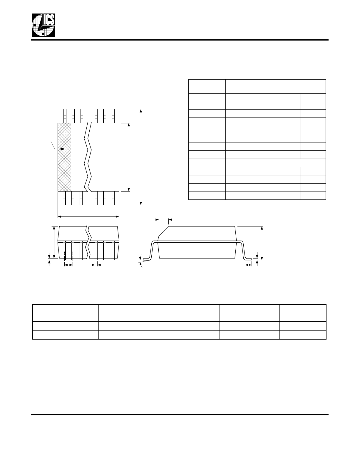
Package Outline and Package Dimensions (20 pin SOIC, 300 Mil. Wide Body)
Package dimensions are kept current with JEDEC Publication No. 95
Millimeters Inches
Symbol Min Max Min Max
A -- 2.65 -- 0.104
A1 1.10 -- 0.0040 -A2 2.05 2.55 0.081 0.100
Ind ex
Area
E
H
B 0.33 0.51 0.013 0.020
C 0.18 0.32 0.007 0.013
D 12.60 13.00 0.496 0.512
E 7.40 7.60 0.291 0.299
e 1.27 Basic 0.050 Basic
H 10.00 10.65 0.394 0.419
h 0.25 0.75 0.010 0.029
L 0.40 1.27 0.016 0.050
α
0
°
8
°
0
°
8
°
A2
A1
12
D
α
Be
h x 45
o
A
C
L
Ordering Information
Part / Order Number Marking Shipping
packaging
MK2059-01SI MK2059-01SI Tubes 20 pin SOIC -40 to +85° C
MK2059-01SITR MK2059-01SI Tape and Reel 20 pin SOIC -40 to +85° C
While the information presented herein has been checked for both accuracy and reliability, Integrated Circuit Systems (ICS)
assumes no responsibility for either its use or for the infringement of any patent s or other rights of third parties, which would
result from its use. No other circuits, patents, or licenses are implied. This product is intended for use in normal commercial
applications. Any oth er ap pl ic ations such as those req uiri ng extended temperat ure ran ge, high reliability, or other extraordina ry
environmental requirements are not recommended without additional processing by ICS. ICS reserves the right to change any
circuitry or specifications without notice. ICS does not authorize or warrant any ICS product for use in life support devices or
critical medical instruments.
Package Temperature
MDS 2059-01 B 10 Revision 071001
Integrated Circuit Systems, Inc. ● 525 Race St reet, San Jose, CA 9512 6 ● tel (408) 295-9800 ● www.icst.com
 Loading...