

Page 1
SUBMINIATURE
PHOTOINTERRUPTER
MIR-3301
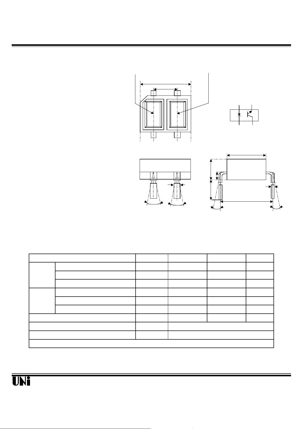
Description Package Dimensions
Unit: mm
The MIR-3301 consists of a Gallium Arsenide infrared emitting diode and a NPN silicon phototransistor built in a black plastic housing. It is a reflective subminiature photointerrupter.
( Emitter center )
3.4±0.2
1.80
A
D
CB
Features
l Compact and thin
l MIR-3301 : Compact DIP, long lead type
l Optimum detecting diatance : 0.8 - 1.0 mm
l Wavelength : 940nm
l Visible light cut-off type
±15°
0.5±0.1
±15°
( Detector center )
0.65
1.5±0.2
10±1.0
0~20° 0~20°
A
B
2.75±0.2
4.0
D
C
0.15
Absolute Maximum Ratings
Parameter Symbol Minimum Rating Maximum Rating Unit
Continuous Forward Current
INPUT Reverse Voltage
Power Dissipation
Collector-emitter breakdown voltage
OUTPUT Emitter-Collector breakdown voltage
Collector power dissipation
Total power dissipation
Operating Temperature Range
Storage Temperature Range
Lead Soldering Temperature (within 5 sec, minimum 1.6mm from body) at 260oC
V
P
V
(BR)CEO
V
(BR)ECO
P
T
I
P
TOT
T
F
ad
C
opr
stg
@ TA=25oC
50 mA
R
5 V
75 mW
30 V
5 V
75 mW
100 mW
o
C to + 85oC
o
C to + 100oC
Unity Opto Technology Co., Ltd.
02/04/2002
Page 2

MIR-3301
Optical-Electrical Characteristics
*2
Device
Ambient Temperature
TOT
Ta=25oC
Forward Voltage
Parameter Min . Typ . Max . Unit . Test Conditions
Input Forward Voltage - 1.2 1.4 V
Reverse Current - - 10 µA
Output Collector Dark Current - - 100 nA Vce=10V
*1
Transfer Cha-
Collector Current
racteristics
Response Time (RISE) - 20 100 µS
Response Time (FALL) - 20 100 µS
Leak Current - - 0.1 µA
Symbol
V
I
Iceo
Ic
t
t
I
LEAK
F
R
B
C
D
E
r
f
38 - 75
56 - 108
80 - 151
112 - 216
µA
IF=20mA
VR=5V
IF=4mA,Vce=5V
Ic=100µA,Vce=2V
RL=1K,d=1mm
IF=4mA,Vce=5V
*1 THE CONDITION AND ARRANGEMENT OF THE REFLECTIVE OBJECT ARE SHOWN AS FOLLOWING .
*2 WITHOUT REFLECTIVE OBJECT.
TEST CONDITION AND ARRANGEMENT FOR COLLECTOR CURRENT
Al refletive
2 mm-thick glass
Typical Optical-Electrical Characteristic Curves
60
(mA)
50
F
40
30
20
10
0
Forward Current I
-25 0 25 50 75 100
Ambient Temperature TA (oC)
Fig.1 forward Current VS
50
(mA)
40
F
30
20
10
0
Forward Current I
0 0.5 1 1.5
Forward Voltage VF (V)
Fig.3 Forward Current VS
.
120
P
100
P
, P
ad
80
60
40
20
0
Power Dissipation (mW)
-25 0 25 50 75 100
C
Ambient Temperature TA ( oC )
Fig.2 Power Dissipation vs.
Ambient Temperature
600
A)
µ
Collector Current Ic (
Vce=5V
500
400
300
200
100
0
0 5 10 15 20
Forward Current IF (mA)
Fig.4 Collector Current vs.
Forward Current
Unity Opto Technology Co., Ltd.
02/04/2002
Page 3

MIR-3301
Typical Optical-Electrical Characteristic Curves
Input
Output
R
Vcc
Ta=25oC
1mA
Collector Dark Current I
CEO
Relative Sensitivity (%)
350
A)
µ
300
250
200
150
100
50
Collector Current Ic (
0
0 2 4 6 8 10 12
4mA
Collector-Emitter Voltage Vce (V)
Fig.5 Collector Current vs. Vce
-6
10
VCE=10V
-7
10
-8
10
-9
10
-10
10
0 25 50 75 100
Ambient Temperature TA (oC)
Fig.7 Collector Dark Current vs.
Ambient Temperature
100
Ta=25oC
80
60
40
20
0
700 800 900 1000 1100 1200
Wavelength (nm)
Fig.9 Spectral Sensitivity (Detecting side)
IF=10mA
120
100
80
60
40
20
0
-25 0 25 50 75 100
Relative Collector Current (%)
Ambient Temperature TA (oC)
Fig.6 Relative Collector Current VS.
100
s)
50
µ
20
10
5
2
1
0.5
Response Time (
0.2
0.1
0.01 0.1 1 10
0.01 0.02 0.05 0.1 0.2 0.5 1 2 5 10
t
r
t
s
t
r
VCE=2V
IC=100μA
Ta=25oC
Load Resistance Rt (KΩ)
Fig.8 Response Time vs.
Load Resistance
120
100
80
60
40
20
0
0 1 2 3 4 5 6 7 8 9 10
Relative Collector Current (%)
IF=4mA
VCE=5V
TA=25oC
Distance (mm)
Fig.10 Relative Collector Current vs. Distance
t
d
Unity Opto Technology Co., Ltd.
Test Circuit for Response Time
R
Input
L
Output
10%
t
90%
f
t
d
t
s
t
r
02/04/2002
 Loading...