

Page 1
MIC5213 Micrel
MIC5213
Teeny™ SC-70 µCap Low-Dropout Regulator
Advance Information
General Description
The MIC5213 is a µCap 80mA linear voltage regulator in the
Teeny™ SC-70 package. Featuring half the footprint of the
standard SOT-23 package, this Teeny SC-70 regulator has
very low dropout voltage (typically 20mV at light loads and
300mV at 80mA) and very low ground current (225µA at
20mA output). It also offers better than 3% initial accuracy
and includes a logic-compatible enable input.
The µCap regulator design is optimized to work with lowvalue, low-cost ceramic capacitors. The outputs typically
require only 0.47µF of output capacitance for stability.
Designed especially for hand-held, battery-powered devices,
the MIC5213 can be controlled by a CMOS or TTL compatible
logic signal. When disabled, power consumption drops nearly
to zero. If on-off control is not required, the enable pin may be
tied to the input for 3-terminal operation. The ground current
of the MIC5213 increases only slightly in dropout, further
prolonging battery life. Key MIC5213 features include current
limiting, overtemperature shutdown, and protection against
reversed battery.
The MIC5213 is available in 2.5V, 2.8V, 3.0V, 3.3V, and 3.6V
fixed voltages. Other voltages are available; contact Micrel
for details.
Features
• Teeny™ SC-70 package
• Wide Selection of output voltages
• Guaranteed 80mA output
• Low quiescent current
• Low dropout voltage
• Tight load and line regulation
• Low temperature coefficient
• Current and thermal limiting
• Reversed input polarity protection
• Zero off-mode current
• Logic-controlled shutdown
• Stability with low-ESR ceramic capacitors
Applications
• Cellular telephones
• Laptop, notebook, and palmtop computers
• Battery-powered equipment
• Bar code scanners
• SMPS post-regulator/dc-to-dc modules
• High-efficiency linear power supplies
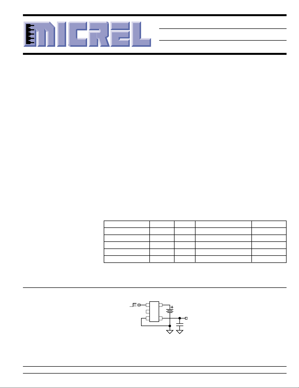
Typical Applications
Ordering Information
Part Number Marking Voltage Junction Temp. Range Package
MIC5213-2.5BC5 LAM 2.5V –40°C to +125°C SC-70-5
MIC5213-2.8BC5 LAJ 2.8V –40°C to +125°C SC-70-5
MIC5213-3.0BC5 LAG 3.0V –40°C to +125°C SC-70-5
MIC5213-3.3BC5 LAE 3.3V –40°C to +125°C SC-70-5
MIC5213-3.6BC5 LAD 3.6V –40°C to +125°C SC-70-5
Other voltages available. Contact Micrel for details.
Enable
Shutdown
15
LAx
2
34
Regulator Circuit
V
OUT
0.47µF
Teeny is a trademark of Micrel, Inc.
Micrel, Inc. • 1849 Fortune Drive • San Jose, CA 95131 • USA • tel + 1 (408) 944-0800 • fax + 1 (408) 944-0970 • http://www.micrel.com
June 2000 1 MIC5213
Page 2
MIC5213 Micrel
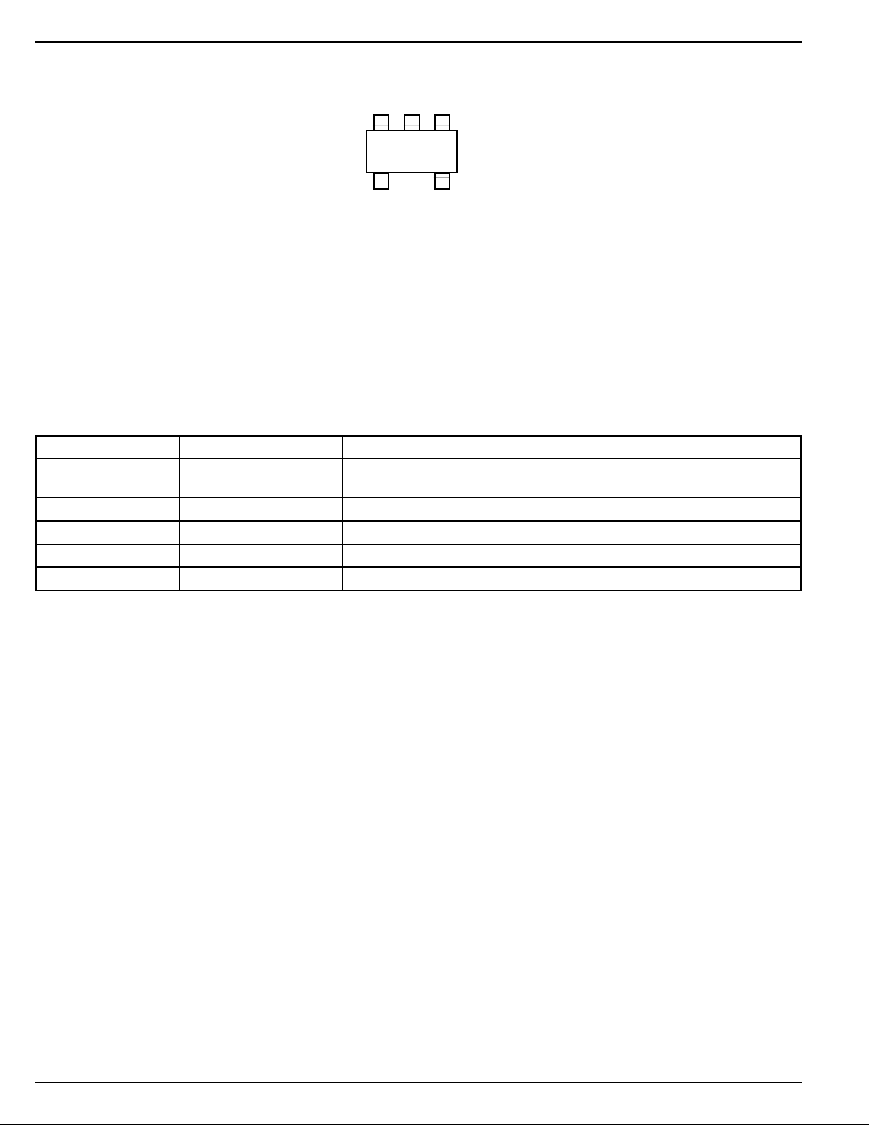
Pin Configuration
Pin Description
Pin Number Pin Name Pin Function
1 EN Enable (Input): TTL/CMOS compatible control input. Logic high = enabled;
2 NC not internally connected
3 GND Ground
4 OUT Regulator Output
5 IN Supply Input
NC
2
EN
13
GND
LAx
45
INOUT
SC-70-5 (C5)
logic low or open = shutdown.
Absolute Maximum Ratings (Note 1)
Input Supply Voltage (VIN) ............................ –20V to +20V
Enable Input Voltage (VEN) ........................... –20V to +20V
Power Dissipation (PD) ............................ Internally Limited
Storage Temperature Range (TS)............–60°C to +150°C
Operating Ratings (Note 2)
Input Voltage (VIN) ........................................... 2.5V to 16V
Enable Input Voltage (VEN) .................................. 0V to V
Junction Temperature Range...................–40°C to +125°C
Thermal Resistance (θJA)......................................... Note 4
IN
Lead Temperature (Soldering, 5 sec.) ...................... 260°C
ESD, Note 3
MIC5213 2 June 2000
Page 3
MIC5213 Micrel
Electrical Characteristics
VIN = V
Symbol Parameter Conditions Min Typ Max Units
V
O
∆VO/∆T Output Voltage Temp. Coefficient Note 5 50 200 ppm/°C
∆V
O/VO
∆V
O/VO
VIN–V
I
Q
I
GND
I
GNDDO
I
LIMIT
∆VO/∆P
Enable Input
V
IL
V
IH
I
IL
I
IH
Note 1. Exceeding the absolute maximum rating may damage the device.
Note 2. The device is not guaranteed to function outside its operating rating.
Note 3. Devices are ESD sensitive. Handling precautions recommended.
Note 4: The maximum allowable power dissipation is a function of the maximum junction temperature, T
Note 5: Output voltage temperature coefficient is defined as the worst case voltage change divided by the total temperature range.
Note 6: Regulation is measured at constant junction temperature using low duty cycle pulse testing. Changes in output voltage due to heating effects
Note 7: Dropout voltage is defined as the input to output differential at which the output voltage drops 2% below its nominal value measured at 1V
Note 8: Ground pin current is the regulator quiescent current plus pass transistor base current. The total current drawn from the supply is the sum of
Note 9: Thermal regulation is defined as the change in output voltage at a time “t” after a change in power dissipation is applied, excluding load or line
+ 1V; IL = 1mA; CL = 0.47µF; V
OUT
≥ 2.0V; TJ = 25°C, bold values indicate –40°C ≤ TJ ≤ +125°C; unless noted.
EN
Output Voltage Accuracy –33%
–44%
Line Regulation VIN = V
+ 1V to 16V 0.008 0.3 %
OUT
0.5 %
Load Regulation IL = 0.1mA to 80mA, Note 6 0.08 0.3 %
0.5 %
O
Dropout Voltage, Note 7 IL = 100µA20mV
IL = 20mA 200 350 mV
IL = 50mA 250 mV
IL = 80mA 300 600 mV
Quiescent Current VEN ≤ 0.4V (shutdown) 0.01 10 µA
Ground Pin Current, Note 8 IL = 100µA, VEN ≥ 2.0V (active) 180 µA
IL = 20mA, VEN ≥ 2.0V (active) 225 750 µA
IL = 50mA, VEN ≥ 2.0V (active) 850 µA
IL = 80mA, VEN ≥ 2.0V (active) 1800 3000 µA
Ground Pin Current at Dropout VIN = V
Current Limit V
D
Thermal Regulation Note 9 0.05 %/W
OUT(nominal)
= 0V 180 250 mA
OUT
– 0.5V, Note 8 200 300 µA
Enable Input Voltage Level logic Low (off) 0.6 V
logic high (on) 2.0 V
Enable Input Current VIL ≤ 0.6V 0.01 1 µA
VIH ≥ 2.0V 15 50 µA
, the junction-to-ambient thermal
resistance, θJA, and the ambient temperature, TA. The maximum allowable power dissipation at any ambient temperature is calculated using:
P
= (T
D(max)
will go into thermal shutdown. θJA of the SC-70-5 is 450°C/W, mounted on a PC board.
are covered by the thermal regulation specification.
differential.
the load current plus the ground pin current.
regulation effects. Specifications are for an 80mA load pulse at VIN = 16V for t = 10ms.
– TA) ÷ θJA. Exceeding the maximum allowable power dissipation will result in excessive die temperature, and the regulator
J(max)
J(max)
June 2000 3 MIC5213
Page 4

MIC5213 Micrel
Typical Characteristics
Dropout Voltage
1000
DROPOUT VOLTAGE (mV)
vs. Output Current
CIN = 10µF
C
= 1µF
OUT
100
10
1
0.01 0.1 1 10 100
OUTPUT CURRENT (mA)
Ground Current
2000
1500
1000
GROUND CURRENT (µA)
vs. Output Current
500
VIN = V
0
0 1020304050607080
OUTPUT CURRENT (mA)
OUT
+ 1V
Dropout Voltage
400
300
200
100
DROPOUT VOLTAGE (mV)
vs. Temperature
CIN = 10µF
C
= 1µF
OUT
IL = 80mA
IL = 1mA
0
-60 -30 0 30 60 90 120 150
TEMPERATURE (°C)
IL = 100µA
Ground Current
vs. Supply Voltage
2.0
1.5
IL = 100µA
1.0
0.5
GROUND CURRENT (mA)
0.0
01234567
IL = 50mA
V
= 3.3V
OUT
SUPPLY VOLTAGE (V)
Dropout
Characteristics
4
IL = 100µA
3
2
1
OUTPUT VOLTAGE (V)
0
01234567
IL = 80mA
CIN = 10µF
C
= 1µF
OUT
SUPPLY VOLTAGE (V)
Ground Current
3.0
2.5
2.0
1.5
1.0
0.5
GROUND CURRENT (mA)
0.0
vs. Temperature
CIN = 10µF
C
= 1µF
OUT
-60 -30 0 30 60 90 120 150
TEMPERATURE (°C)
IL = 80mA
IL = 50mA
IL = 100µA
Output Voltage
vs. Output Current
4.0
3.5
3.0
2.5
CIN = 10µF
C
2.0
1.5
1.0
OUTPUT VOLTAGE (V)
0.5
0.0
= 1µF
OUT
0 50 100 150 200
OUTPUT CURRENT (mA)
Output Voltage
4.0
3.8
3.6
3.4
3.2
3.0
2.8
OUTPUT VOLTAGE (V)
2.6
2.4
vs. Temperature
CIN = 10µF
C
= 1µF
OUT
3 DEVICES
HI / AVG / LO
CURVES APPLICABLE
AT 100µA AND 50mA
-60 -30 0 30 60 90 120 150
TEMPERATURE (°C)
Short Circuit Current
160
140
120
100
SHORT CIRCUIT CURRENT (mA)
vs. Input Voltage
80
60
40
20
0
01234567
INPUT VOLTAGE (V)
CIN = 10µF
C
= 1µF
OUT
Short Circuit Current
200
180
160
140
120
OUTPUT CURRENT (mA)
100
vs. Temperature
CIN = 10µF
C
= 1µF
OUT
-60 -30 0 30 60 90 120 150
TEMPERATURE (°C)
Thermal Regulation
60
40
20
-20
-40
∆ OUTPUT (mV)
-60
100
50
LOAD (mA)
-50
(3.3V Version)
0
0
CL = 1µF
-2 0 2 4 6 8 10 12 14 16
TIME (ms)
Minimum Supply Voltage
3.5
3.4
MIN. SUPPLY VOLTAGE (V)
3.3
vs. Temperature
IL = 1mA
V
= 3.3V
OUT
CIN = 10µF
C
= 1µF
OUT
-60 -30 0 30 60 90 120 150
TEMPERATURE (°C)
MIC5213 4 June 2000
Page 5

MIC5213 Micrel
-400
-200
0
200
∆ OUTPUT (mV)
-50
0
50
100
-1 012345678
OUTPUT (mA)
TIME (ms)
-2
-1
0
1
2
3
∆ OUTPUT (V)
2
4
6
8
-0.2 0.0 0.2 0.4 0.6 0.8 1.0
INPUT (V)
TIME (ms)
0
20
40
60
80
100
10x10
0
100x10
0
1x10
3
10x10
3
100x10
3
1x10
6
RIPPLE VOLTAGE (dB)
FREQUENCY (Hz)
Load Transient
C
= 1µF
OUT
V
= V
IN
Line Transient
CL = 1µF
I
= 1mA
L
OUT
+ 1
100
Load Transient
0
C
= 10µF
-100
∆ OUTPUT (mV)
100
-200
OUT
V
= V
IN
OUT
50
0
OUTPUT (mA)
-50
-5 0 5 10 15 20
2
1
TIME (ms)
Line Transient
CL = 11µF
I
= 1mA
L
0
∆ OUTPUT (V)
8
-1
6
4
INPUT (V)
2
-0.2 0.0 0.2 0.4 0.6 0.8 1.0
TIME (ms)
+ 1
100
80
60
40
20
RIPPLE VOLTAGE (dB)
0
0
10x10
June 2000 5 MIC5213
Ripple Voltage
vs. Frequency
IL = 100µA
C
= 1µF
L
V
= V
+ 1
IN
OUT
0
3
1x10
100x10
FREQUENCY (Hz)
3
10x10
3
100x10
6
1x10
Ripple Voltage
vs. Frequency
IL = 1mA
C
= 1µF
L
V
= V
+ 1
IN
OUT
Ripple Voltage
0
IL = 50mA
C
V
0
10x10
vs. Frequency
= 1µF
L
= V
+ 1
IN
OUT
0
3
1x10
100x10
FREQUENCY (Hz)
100
80
60
40
20
RIPPLE VOLTAGE (dB)
3
10x10
3
100x10
6
1x10
Page 6

MIC5213 Micrel
1000
100
0.1
OUTPUT IMPEDANCE (Ω)
0.01
Output Impedance
IL = 100µA
10
IL = 1mA
1
0
0
1x10
10x10
FREQUENCY (Hz)
0
100x10
IL = 100mA
3
3
1x10
10x10
3
100x10
6
1x10
Enable Characteristics
(3.3V Version)
5
4
3
2
1
0
OUTPUT (V)
4
-1
CL = 1µF
I
= 100µA
L
2
0
ENABLE (V)
-2
-0.2 0.0 0.2 0.4 0.6 0.8 1.0
TIME (ms)
Enable Voltage
1.50
1.25
1.00
0.75
ENABLE VOLTAGE (mV)
0.50
vs. Temperature
CIN = 10µF
C
= 1µF
OUT
I
= 1mA
L
V
OFF
ON
V
-60 -30 0 30 60 90 120 150
TEMPERATURE (°C)
Enable Characteristics
4.0
3.0
2.0
1.0
0.0
OUTPUT (V)
-1.0
ENABLE (V)
(3.3V Version)
CL = 1µF
I
= 100µA
4
2
0
-2
-2 0246810
L
TIME (µs)
Enable Current
vs. Temperature
40
30
20
10
ENABLE CURRENT (µA)
0
-60 -30 0 30 60 90 120 150
TEMPERATURE (°C)
VEN = 2V
CIN = 10µF
C
= 1µF
OUT
I
= 1mA
L
VEN = 5V
MIC5213 6 June 2000
Page 7

MIC5213 Micrel
P
125 25
450 C/W
D(max)
=
−
°
Applications Information
Input Capacitor
A 0.1µF capacitor should be placed from IN to GND if there
is more than 10 inches of wire between the input and the ac
filter capacitor or when a battery is used as the input.
Output Capacitor
Typical PNP based regulators require an output capacitor to
prevent oscillation. The MIC5213 is ultrastable, requiring only
0.47µF of output capacitance for stability. The regulator is
stable with all types of capacitors, including the tiny, low-ESR
ceramic chip capacitors. The output capacitor value can be
increased without limit to improve transient response.
No-Load Stability
The MIC5213 will remain stable and in regulation with no load
(other than the internal voltage divider) unlike many other
voltage regulators. This is especially important in CMOS
RAM keep-alive applications.
Enable Input
The MIC5213 features nearly zero off-mode current. When
EN (enable input) is held below 0.6V, all internal circuitry is
powered off. Pulling EN high (over 2.0V) re-enables the
device and allows operation. When EN is held low, the
regulator typically draws only 10nA of current. While the logic
threshold is TTL/CMOS compatible, EN may be pulled as
high as 20V, independent of VIN.
Thermal Behavior
The MIC5213 is designed to provide 80mA of continuous
current in a very small profile packages. Maximum power
dissipation can be calculated based on the output current and
the voltage drop across the part. To determine the maximum
power dissipation of the package, use the junction-to-ambient thermal resistance of the device and the following basic
equation:
TT
T
J(max)
P
=
D(max)
is the maximum junction temperature of the die,
125°C, and TA is the maximum ambient temperature. θJA is
the junction-to-ambient thermal resistance ambient of the
regulator. The θJA of the MIC5213 is 450°C/W.
−
J(max) A
θ
JA
The actual power dissipation of the regulator circuit can be
determined using one simple equation.
= (VIN – V
P
D
Substituting P
D(max)
) I
OUT
+ VIN × I
GND
OUT
, determined above, for PD and solving
for the operating conditions that are critical to the application
will give the maximum operating conditions for the regulator
circuit. For example, if we are operating the MIC5213-3.0BC5
at room temperature, with a minimum footprint layout, we can
determine the maximum input voltage for a set output current.
P 222mW
D(max)
=
To prevent the device from entering thermal shutdown,
maximum power dissipation cannot be exceeded. Using the
output voltage of 3.0V, and an output current of 80mA, we can
determine the maximum input voltage. Ground current, maximum of 3mA for 80mA of output current, can be taken from
the “Electrical Characteristics” section of the data sheet.
222mW = (VIN – 3.0V) 80mA + VIN × 3mA
222mW = (80mA × VIN + 3mA × VIN) – 240mW
462mW = 83mA × V
IN
VIN = 5.57V max.
Therefore, a 3.0V application at 80mA of output current can
accept a maximum input voltage of 5.6V in an SC-70-5
package. For a full discussion of heat sinking and thermal
effects on voltage regulators, refer to Regulator Thermals
section of Micrel’s
lators
handbook.
Designing with Low-Dropout Voltage Regu-
Fixed Voltage Regulator
The MIC5213 is ideal for general-purpose voltage regulation
in any handheld device. Applications that are tight for space
can easily use the Teeny™ SC-70 regulator which occupies
half the space of a SOT-23-5 regulator. The MIC5203 offers
a smaller system solution, only requiring a small multilayer
ceramic capacitor for stability.
V
OUT
3.0V
0.47µF
3.6V
Li-Ion
Cell
MIC5213-x.x
IN OUT
EN
GND
Figure 1. Single-Cell Regulator
June 2000 7 MIC5213
Page 8

MIC5213 Micrel
Package Information
0.65 (0.0256) BSC
2.20 (0.087)
1.80 (0.071)
0.30 (0.012)
0.15 (0.006)
1.35 (0.053)
1.15 (0.045)
1.00 (0.039)
0.80 (0.032)
0.10 (0.004)
0.00 (0.000)
SC-70-5 (C5)
2.40 (0.094)
1.80 (0.071)
1.10 (0.043)
0.80 (0.032)
DIMENSIONS:
MM (INCH)
0.18 (0.007)
0.10 (0.004)
0.30 (0.012)
0.10 (0.004)
MICREL INC. 1849 FORTUNE DRIVE SAN JOSE, CA 95131 USA
TEL + 1 (408) 944-0800 FAX + 1 (408) 944-0970 WEB http://www.micrel.com
This information is believed to be accurate and reliable, however no responsibility is assumed by Micrel for its use nor for any infringement of patents or
other rights of third parties resulting from its use. No license is granted by implication or otherwise under any patent or patent right of Micrel Inc.
© 2000 Micrel Incorporated
MIC5213 8 June 2000
 Loading...