

Datasheet MIC5211-5.0BM6, MIC5211-3.3BM6, MIC5211-3.0BM6, MIC5211-3.3-5.0BM6, MIC5211-2.5BM6 Datasheet (MICREL)
...Page 1
MIC5211 Micrel
MIC5211
Dual µCap 80mA LDO Regulator
Preliminary Information
General Description
The MIC5211 is a dual µCap 80mA linear voltage regulator
with very low dropout voltage (typically 20mV at light loads),
very low ground current (225µA at 20mA output current), and
better than 3% initial accuracy. This dual device comes in the
miniature SOT-23-6 package, featuring independent logic
control inputs.
The µCap regulator design is optimized to work with lowvalue, low-cost ceramic capacitors. The outputs typically
require only 0.1µF of output capacitance for stability.
Designed especially for hand-held, battery-powered devices,
ground current is minimized using Micrel’s proprietary Super
ßeta PNP™ technology to prolong battery life. When disabled, power consumption drops nearly to zero.
Key features include SOT-23-6 packaging, current limiting,
overtemperature shutdown, and protection against reversed
battery conditions.
The MIC5211 is available in dual 1.8V, 2.5V, 2.7V, 2.8V,
3.0V, 3.3V, 3.6V, and 5.0V versions. Certain mixed voltages
are also available. Contact Micrel for other voltages.
Ordering Information
Features
• Stable with low-value ceramic or tantalum capacitors
• Independent logic controls
• Low quiescent current
• Low dropout voltage
• Mixed voltages available
• Tight load and line regulation
• Low temperature coefficient
• Current and thermal limiting
• Reversed input polarity protection
• Zero off-mode current
• Dual regulator in tiny SOT-23 package
• 2.5V to 16V input range
Applications
• Cellular telephones
• Laptop, notebook, and palmtop computers
• Battery-powered equipment
• Bar code scanners
• SMPS post regulator/dc-to-dc modules
• High-efficiency linear power supplies
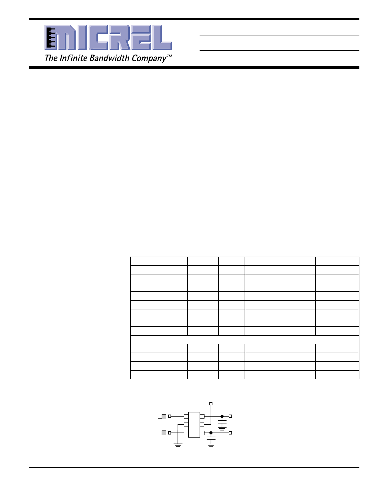
Typical Application
Part Number Marking Voltage Junction Temp. Range Package
MIC5211-1.8BM6 LFBB 1.8V 0°C to +125°C SOT-23-6
MIC5211-2.5BM6 LFCC 2.5V –40°C to +125°C SOT-23-6
MIC5211-2.7BM6 LFDD 2.7V –40°C to +125°C SOT-23-6
MIC5211-2.8BM6 LFEE 2.8V –40°C to +125°C SOT-23-6
MIC5211-3.0BM6 LFGG 3.0V –40°C to +125°C SOT-23-6
MIC5211-3.3BM6 LFLL 3.3V –40°C to +125°C SOT-23-6
MIC5211-3.6BM6 LFQQ 3.6V –40°C to +125°C SOT-23-6
MIC5211-5.0BM6 LFXX 5.0V –40°C to +125°C SOT-23-6
Dual-Voltage Regulators
MIC5211-1.8/2.5BM6 LFBC 1.8V/2.5V 0°C to +125°C SOT-23-6
MIC5211-1.8/3.3BM6 LFBL 1.8V/3.3V 0°C to +125°C SOT-23-6
MIC5211-2.5/3.3BM6 LFCL 2.5V/3.3V –40°C to +125°C SOT-23-6
MIC5211-3.3/5.0BM6 LFLX 3.3V/5.0V –40°C to +125°C SOT-23-6
Other voltages available. Contact Micrel for details.
V
IN
MIC5211
Enable
Shutdown
Enable
Shutdown
Enable A
Enable B
16
2
3
5
4
0.1µF
V
0.1µF
V
OUTA
OUTB
Micrel, Inc. • 1849 Fortune Drive • San Jose, CA 95131 • USA • tel + 1 (408) 944-0800 • fax + 1 (408) 944-0970 • http://www.micrel.com
November 2000 1 MIC5211
Page 2
MIC5211 Micrel
Pin Configuration
OUTA
IN
OUTB
46
5
Pin 1
Index
LFxx
13
2
ENA GND
Regulator A
Voltage Code
(V
OUTA
)
Part
Identification
ENB
Regulator B
Voltage Code
(V
OUTB
egatloVedoC
V8.1B
V5.2C
V7.2D
V8.2E
V3G
V51.3H
V3.3L
V6.3Q
V5X
)
Pin Description
Pin Number Pin Name Pin Function
1 ENA Enable/Shutdown A (Input): CMOS compatible input. Logic high = enable,
2 GND Ground
3 ENB Enable/Shutdown B (Input): CMOS compatible input. Logic high = enable,
4 OUTB Regulator Output B
5 IN Supply Input
6 OUTA Regulator Output A
logic low or open = shutdown.
logic low or open = shutdown.
MIC5211 2 November 2000
Page 3
MIC5211 Micrel
Absolute Maximum Ratings (Note 1)
Supply Input Voltage (VIN) ............................ –20V to +20V
Enable Input Voltage (V
Power Dissipation (P
Storage Temperature Range ................... –60°C to +150°C
Lead Temperature (soldering, 5 sec.) ....................... 260°C
) ........................... –20V to +20V
EN
) ............................Internally Limited
D
Operating Ratings (Note 2)
Supply Input Voltage (VIN) ............................... 2.5V to 16V
Enable Input Voltage (V
Junction Temperature (T
1.8V only .................................................. 0°C to +125°C
6-lead SOT-23-6 (θJA).............................................. Note 4
) ................................. 0V to 16V
EN
) (except 1.8V). –40°C to +125°C
J
ESD, (Note 3) .....................................................................
Electrical Characteristics
VIN = V
for one-half of dual MIC5211; unless noted.
Symbol Parameter Conditions Min Typical Max Units
V
O
∆V
O
∆V
O/VO
∆V
O/VO
VIN – V
I
Q
I
GND
I
LIMIT
∆VO/∆P
Enable Input
V
IL
V
IH
I
IL
I
IH
Note 1: Exceeding the absolute maximum rating may damage the device.
Note 2: The device is not guareented to function outside itsperating rating.
Note 3: Devices are ESD sensitive. Handling precautions recommended.
Note 4: The maximum allowable power dissipation at any TA (ambient temperature) is P
Note 5: Output voltage temperature coeffiecient is defined as the worst case voltage change divided by the total temperature range.
Note 6: Regulation is measured at constant junction temperature using low duty cycle pulse testing. Parts are tested for load regulation in the load
Note 7: Dropout voltage is defined as the input to output differential at which the output voltage drops 2% below its nominal value measured at 1V
Note 8: Ground pin current is the quiescent current per regulator plus pass transistor base current. The total current drawn from the supply is the sum
Note 9: Thermal regulation is defined as the change in output voltage at a time “t” after a change in power dissipation is applied, excluding load or line
+ 1V; IL = 1mA; CL = 0.1µF, and V
OUT
Output Voltage variation from nominal V
Accuracy –44%
≥ 2.0V; TJ = 25°C, bold values indicate –40°C to +125°C;
EN
OUT
–33%
/∆T Output Voltage Note 5 50 200 ppm/°C
Temperature Coeffcient
Line Regulation VIN = V
+1V to 16V 0.008 0.3 %
OUT
0.5 %
Load Regulation IL = 0.1mA to 50mA, Note 6 0.08 0.3 %
0.5 %
O
Dropout Voltage, Note 7 IL = 100µA20mV
IL = 20mA 200 450 mV
IL = 50mA 250 500 mV
Quiescent Current VEN ≤ 0.4V (shutdown) 0.01 10 µA
Ground Pin Current VEN ≥ 2.0V, IL = 100µA (active) 90 µA
Note 8 IL = 20mA (active) 225 450 µA
IL = 50mA (active) 750 1200 µA
Current Limit V
D
Thermal Regulation Note 9 0.05 %/W
= 0V 140 250 mA
OUT
Enable Input Voltage Level
logic low (off) 0.6 V
logic high (on) 2.0 V
Enable Input Current VIL ≤ 0.6V 0.01 1 µA
VIH ≥ 2.0V 3 50 µA
= (T
allowable power dissipation will result in excessive die temperature, and the regulator will go into thermal shutdown. The θJA is 220°C/W for
the SOT-23-6 mounted on a printed circuit board.
range from 0.1mA to 50mA. Change in output voltage due to heating effects are covered by thermal regulation specification.
differential. For output voltages below 2.5V, dropout voltage is the input-to-output voltage differential with the minimum voltage being 2.5V.
Minimum input opertating voltage is 2.5V.
of the load current plus the ground pin current.
regulation effects. Specifications are for a 50mA load pulse at VIN = 16V for t = 10ms.
D(max)
– TA) / θJA. Exceeding the maximum
J(max)
November 2000 3 MIC5211
Page 4
MIC5211 Micrel
Typical Characteristics
Dropout Voltage
1000
DROPOUT VOLTAGE (V)
vs. Output Current
CIN = 10µF
C
= 1µF
OUT
100
10
1
0.01 0.1 1 10 100
OUTPUT CURRENT (mA)
Ground Current
2000
1500
1000
GROUND CURRENT (µA)
vs. Output Current
500
VIN = V
0
0 1020304050607080
OUTPUT CURRENT (mA)
OUT
+ 1V
Dropout Voltage
400
300
200
100
DROPOUT VOLTAGE (mV)
vs. Temperature
CIN = 10µF
C
= 1µF
OUT
IL = 50mA
IL = 1mA
0
-60 -30 0 30 60 90 120 150
TEMPERATURE (°C)
IL = 100µA
Ground Current
vs. Supply Voltage
2.0
1.5
IL = 100µA
1.0
0.5
GROUND CURRENT (mA)
0.0
01234567
IL = 50mA
V
= 3.3V
OUT
SUPPLY VOLTAGE (V)
Dropout Characteristics
4
3
2
1
OUTPUT VOLTAGE (V)
0
(MIC5211-3.3)
IL = 100µA
IL = 50mA
CIN = 10µF
C
= 1µF
OUT
01234567
SUPPLY VOLTAGE (V)
Ground Current
3.0
2.5
2.0
1.5
1.0
0.5
GROUND CURRENT (mA)
0.0
vs. Temperature
CIN = 10µF
C
= 1µF
OUT
IL = 50mA
IL = 100µA
-60 -30 0 30 60 90 120 150
TEMPERATURE (°C)
Output Voltage
vs. Output Current
4.0
3.5
3.0
2.5
CIN = 10µF
C
2.0
1.5
1.0
OUTPUT VOLTAGE (V)
0.5
0.0
= 1µF
OUT
0 50 100 150 200
OUTPUT CURRENT (mA)
Short Circuit Current
160
140
120
100
SHORT CIRCUIT CURRENT (mA)
vs. Input Voltage
80
60
40
20
0
01234567
INPUT VOLTAGE (V)
CIN = 10µF
C
= 1µF
OUT
Short Circuit Current
200
180
160
140
120
OUTPUT CURRENT (mA)
100
vs. Temperature
CIN = 10µF
C
= 1µF
OUT
-60 -30 0 30 60 90 120 150
TEMPERATURE (°C)
Output Voltage
4.0
3.8
3.6
3.4
3.2
3.0
2.8
OUTPUT VOLTAGE (V)
2.6
2.4
vs. Temperature
CIN = 10µF
C
= 1µF
OUT
3 DEVICES
HI / AVG / LO
CURVES APPLICABLE
AT 100µA AND 50mA
-60 -30 0 30 60 90 120 150
TEMPERATURE (°C)
MIC5211 4 November 2000
Page 5

MIC5211 Micrel
0
20
40
60
80
100
10x10
0
100x10
0
1x10
3
10x10
3
100x10
3
1x10
6
RIPPLE VOLTAGE (dB)
FREQUENCY (Hz)
200
Load Transient
0
C
-200
∆ OUTPUT (mV)
100
-400
= 1µF
OUT
V
= V
IN
OUT
50
0
OUTPUT (mA)
-50
-1 012345678
TIME (ms)
Line Transient
(MIC5211-3.3)
3
2
1
0
-1
∆ OUTPUT (V)
8
-2
6
4
INPUT (V)
2
-0.2 0.0 0.2 0.4 0.6 0.8 1.0
CL = 1µF
I
= 1mA
L
TIME (ms)
+ 1
100
Load Transient
0
C
= 10µF
-100
∆ OUTPUT (mV)
100
-200
OUT
V
= V
IN
OUT
50
0
OUTPUT (mA)
-50
-5 0 5 10 15 20
TIME (ms)
Line Transient
(MIC5211-3.3)
2
1
0
∆ OUTPUT (V)
8
-1
6
4
INPUT (V)
2
-0.2 0.0 0.2 0.4 0.6 0.8 1.0
CL = 11µF
I
= 1mA
L
TIME (ms)
+ 1
Ripple Voltage
100
80
60
40
20
RIPPLE VOLTAGE (dB)
0
vs. Frequency
IL = 100µA
C
= 1µF
L
V
= V
IN
0
0
10x10
100x10
FREQUENCY (Hz)
OUT
+ 1
3
1x10
3
10x10
3
100x10
6
1x10
Ripple Voltage
vs. Frequency
IL = 1mA
C
= 1µF
L
V
= V
+ 1
IN
OUT
Ripple Voltage
0
IL = 50mA
C
V
0
10x10
vs. Frequency
= 1µF
L
= V
+ 1
IN
OUT
0
3
1x10
100x10
FREQUENCY (Hz)
100
80
60
40
20
RIPPLE VOLTAGE (dB)
3
10x10
3
100x10
6
1x10
November 2000 5 MIC5211
Page 6

MIC5211 Micrel
1000
Output Impedance
100
IL = 100µA
10
IL = 1mA
1
0.1
IL = 50mA
OUTPUT IMPEDANCE (Ω)
0.01
0
1x10
0
10x10
3
0
FREQUENCY (Hz)
100x10
1x10
3
10x10
Minimum Supply Voltage
3.5
3.4
MIN. SUPPLY VOLTAGE (V)
3.3
vs. Temperature
IL = 1mA
V
= 3.3V
OUT
CIN = 10µF
C
= 1µF
OUT
-60 -30 0 30 60 90 120 150
TEMPERATURE (°C)
3
100x10
6
1x10
Enable Characteristics
4.0
3.0
2.0
1.0
0.0
OUTPUT (V)
-1.0
ENABLE (V)
(MIC5211-3.3)
CL = 1µF
I
= 100µA
4
2
0
-2
-2 0246810
L
TIME (µs)
Enable Voltage
1.50
1.25
1.00
0.75
ENABLE VOLTAGE (mV)
0.50
vs. Temperature
CIN = 10µF
C
= 1µF
OUT
I
= 1mA
L
V
OFF
ON
V
-60 -30 0 30 60 90 120 150
TEMPERATURE (°C)
Enable Characteristics
(MIC5211-3.3)
5
4
3
2
1
0
OUTPUT (V)
4
-1
CL = 1µF
I
= 100µA
L
2
0
ENABLE (V)
-2
-0.2 0.0 0.2 0.4 0.6 0.8 1.0
TIME (ms)
Enable Current
vs. Temperature
40
30
20
10
ENABLE CURRENT (µA)
0
-60 -30 0 30 60 90 120 150
TEMPERATURE (°C)
VEN = 2V
CIN = 10µF
C
= 1µF
OUT
I
= 1mA
L
VEN = 5V
OUTA
V
OUTB
V
OUTA
I
Crosstalk Characteristic
(50mV/div.)
I
= 100µA
OUTB
= 0.47µF
C
OUTB
= 0.47µF
C
OUTA
(50mV/div.)
(50mA/div.)
TIME (25ms/div.)
MIC5211 6 November 2000
Page 7

MIC5211 Micrel
P
125 C 25 C
220 C/W
D(max)
=
°− °
°
P P 106.8mW
D1 D2
+=
P
125 C 70 C
220 C/W
D(max)
=
°− °
°
Applications Information
Enable/Shutdown
ENA and ENB (enable/shutdown) may be controlled separately. Forcing ENA/B high (>2V) enables the regulator. The
enable inputs typically draw only 15µA.
While the logic threshold is TTL/CMOS compatible, ENA/B
may be forced as high as 20V, independent of V
may be connected to the supply if the function is not required.
Input Capacitor
A 0.1µF capacitor should be placed from IN to GND if there
is more than 10 inches of wire between the input and the ac
filter capacitor or when a battery is used as the input.
Output Capacitor
Typical PNP based regulators require an output capacitor to
prevent oscillation. The MIC5211 is ultrastable, requiring only
0.1µF of output capacitance per regulator for stability. The
regulator is stable with all types of capacitors, including the
tiny, low-ESR ceramic chip capacitors. The output capacitor
value can be increased without limit to improve transient
response.
The capacitor should have a resonant frequency above
500kHz. Ceramic capacitors work, but some dielectrics have
poor temperature coefficients, which will affect the value of
the output capacitor over temperature. Tantalum capacitors
are much more stable over temperature, but typically are
larger and more expensive. Aluminum electrolytic capacitors
will also work, but they have electrolytes that freeze at about
–30°C. Tantalum or ceramic capacitors are recommended
for operation below –25°C.
No-Load Stability
The MIC5211 will remain stable and in regulation with no load
(other than the internal voltage divider) unlike many other
voltage regulators. This is especially important in CMOS
RAM keep-alive applications.
Thermal Shutdown
Thermal shutdown is independent on both halves of the dual
MIC5211, however, an overtemperature condition in one half
may affect the other half because of proximity.
Thermal Considerations
When designing with a dual low-dropout regulator, both
sections must be considered for proper operation. The part is
designed with thermal shutdown, therefore, the maximum
junction temperature must not be exceeded. Since the dual
regulators share the same substrate, the total power dissipation must be considered to avoid thermal shutdown. Simple
thermal calculations based on the power dissipation of both
regulators will allow the user to determine the conditions for
proper operation.
The maximum power dissipation for the total regulator system can be determined using the operating temperatures and
the thermal resistance of the package. In a minimum footprint
configuration, the SOT-23-6 junction-to-ambient thermal resistance (θ
) is 220°C/W. Since the maximum junction
JA
temperature for this device is 125°C, at an operating temperature of 25°C the maximum power dissipation is:
. ENA/B
IN
P
P 455mW
D(max)
D(max)
=
=
TT
−
J(max) A
θ
JA
The MIC5211-3.0 can supply 3V to two different loads independently from the same supply voltage. If one of the regulators is supplying 50mA at 3V from an input voltage of 4V, the
total power dissipation in this portion of the regulator is:
PVVI VI
=−
()
D1 IN
P 4V 3V 50mA 4V 0.85mA
=−
()
D1
P 53.4mW
=
D1
OUT OUT
+⋅
IN
+⋅
GND
Up to approximately 400mW can be dissipated by the remaining regulator (455mW – 53.4mW) before reaching the thermal shutdown temperature, allowing up to 50mA of current.
PVVI VI
=−
()
D2 IN
P 4V 3V 50mA 4V 0.85mA
=−
()
D2
P 53.4mW
=
D2
OUT OUT
+⋅
IN
+⋅
GND
The total power dissipation is:
P P 53.4mW 53.4mW
+= +
D1 D2
Therefore, with a supply voltage of 4V, both outputs can
operate safely at room temperature and full load (50mA).
V
IN
MIC5211
V
1µF
OUTA
V
OUTB
IN OUTA
ENA OUTB
GND
ENB
1µF
Figure 1. Thermal Conditions Circuit
In many applications, the ambient temperature is much
higher. By recalculating the maximum power dissipation at
70°C ambient, it can be determined if both outputs can supply
full load when powered by a 4V supply.
P
P 250mW
D(max)
D(max)
=
=
TT
−
J(max) A
θ
JA
At 70°C, the device can provide 250mW of power dissipation,
suitable for the above application.
When using supply voltages higher than 4V, do not exceed
the maximum power dissipation for the device. If the device
November 2000 7 MIC5211
Page 8

MIC5211 Micrel
is operating from a 7.2V-nominal two-cell lithium-ion battery
and both regulators are dropping the voltage to 3.0V, then
output current will be limited at higher ambient temperatures.
For example, at 70°C ambient the first regulator can supply
3.0V at 50mA output from a 7.2V supply; however, the
second regulator will have limitations on output current to
avoid thermal shutdown. The dissipation of the first regulator
is:
=−
P 7.2V 3V 50mA 7.2V 0.85mA
()
D1
P 216mW
=
D1
+⋅
Since maximum power dissipation for the dual regulator is
250mW at 70°C, the second regulator can only dissipate up
to 34mW without going into thermal shutdown. The amount
of current the second regulator can supply is:
P 34mW
D2(max)
7.2V 3V I 34mW
()
4.2V I 34mW
I8mA
OUT2(max)
=
−
OUT2(max)
⋅=
OUT2(max)
=
=
The second regulator can provide up to 8mA output current,
suitable for the keep-alive circuitry often required in handheld applications.
Refer to Application Hint 17 for heat sink requirements when
higher power dissipation capability is needed. Refer to
signing with Low Dropout Voltage Regulators
for a more
De-
thorough discussion of regulator thermal characteristics.
Dual-Voltage Considerations
For configurations where two different voltages are needed in
the system, the MIC5211 has the option of having two
independent output voltages from the same input. For example, a 3.3V rail and a 5.0V rail can be supplied from the
MIC5211 for systems that require both voltages. Important
considerations must be taken to ensure proper functionality
of the part. The input voltage must be high enough for the 5V
section to operate correctly, this will ensure the 3.3V section
proper operation as well.
Both regulators live off of the same input voltage, therefore
the amount of output current each regulator supplies may be
limited thermally. The maximum power the MIC5211 can
dissipate at room temperature is 455mW, as shown in the
“Thermal Considerations” section. If we assume 6V input
voltage and 50mA of output current for the 3.3V section of the
regulator, then the amount of output current the 5V section
can provide can be calculated based on the power dissipation.
PD = (V
P
D(3.3V)
P
D(3.3V)
P
D(max)
P
D(max)
P
D(5V)
P
D(5V)
GND
– V
OUT
) I
OUT
+ V
GND
· I
GND
= (6V – 3.3V) 50mA + 6V · 0.85mA
= 140.1mW
= 455mW
– P
D(3.3V)
= P
D(5V)
= 455mW – 140.1mW
= 314.9mW
Based on the power dissipation allowed for the 5V section,
the amount of output current it can source is easily calculated.
P
= 314.9mW
D(5V)
314.9mW = (6V – 5V) I
(I
typically adds less than 5% to the total power dissipa-
GND
MAX
– 6V · I
GND
tion and in this case can be ignored)
314.9mW = (6V – 5V) I
I
= 314.9mA
MAX
I
exceeds the maximum current rating of the device.
MAX
MAX
Therefore, for this condition, the MIC5211 can supply 50mA
of output current from each section of the regulator.
MIC5211 8 November 2000
Page 9

MIC5211 Micrel
Package Information
1.90 (0.075) REF
0.95 (0.037) REF
3.00 (0.118)
2.80 (0.110)
0.50 (0.020)
0.35 (0.014)
1.75 (0.069)
1.50 (0.059)
1.30 (0.051)
0.90 (0.035)
0.15 (0.006)
0.00 (0.000)
SOT-23-6 (M6)
3.00 (0.118)
2.60 (0.102)
10°
0°
DIMENSIONS:
MM (INCH)
0.20 (0.008)
0.09 (0.004)
0.60 (0.024)
0.10 (0.004)
November 2000 9 MIC5211
Page 10

MIC5211 Micrel
MIC5211 10 November 2000
Page 11

MIC5211 Micrel
November 2000 11 MIC5211
Page 12

MIC5211 Micrel
MICREL INC. 1849 FORTUNE DRIVE SAN JOSE, CA 95131 USA
TEL + 1 (408) 944-0800 FAX + 1 (408) 944-0970 WEB http://www.micrel.com
This information is believed to be accurate and reliable, however no responsibility is assumed by Micrel for its use nor for any infringement of patents or
other rights of third parties resulting from its use. No license is granted by implication or otherwise under any patent or patent right of Micrel Inc.
© 2000 Micrel Incorporated
MIC5211 12 November 2000
 Loading...